1. Introduction
Metal wafer bonding combines silicon wafers with different materials through chemical and physical interactions [
1]. It is widely used in materials manufacturing, device integration, and product packaging [
2,
3,
4,
5]. The main techniques used for metal wafer bonding include eutectic bonding and transient liquid phase bonding (TLP). TLP bonding is often used when high-reliability bond lines or electric connections are needed [
6]. In this process, the interlayer melts, and the interlayer element diffuses into the substrate materials, causing isothermal solidification. In TLP, it is important to select a suitable interlayer based on the flow characteristics, stability, and wettability to form a composition that provides faster diffusion characteristics and high reliability [
7]. Therefore, a high level of welding technology and cost is required to achieve TLP. Compared with complex TLP, eutectic bonding has fewer constraints, easy formation of ohmic contact at the interface, small parasitic parameters, low bonding temperature, low residual force, ease of implementation, and high accuracy in patterning. Eutectic bonding is the process by which two metals are fused into an alloy and solidified so that the mixture can form a crystalline structure after re-solidification [
8]. During eutectic bonding, the metal layers on the substrate are fused to each other at a specific temperature. The melting of the metallic material causes the layers to mix and consume faster at the bonding surface, and the metal can form a fluid state that flattens the area at the interface. Eventually, a stable molten metallic phase can be formed at the interface. Therefore, Wang et al. exploited the low melting temperature of Au-Si eutectic alloys and used them as an intermediate dielectric layer to produce a metal-semiconductor eutectic phase by heating and melting at a lower temperature to achieve bonding [
9]. Zhang et al. also realized low-temperature eutectic bonding for hermetic packages of MEMS devices [
10].
Aluminum (Al) wafer bonding technology is insensitive to oxides on the wafer surface, has high thermal and electrical conductivity, and is compatible with the silicon IC industry. Consequently, Al wafer bonding technology has attracted the attention of countless researchers [
11,
12,
13,
14]. Malik et al. [
15] studied Al-Al direct bonding using different bonding temperatures (400 °C, 450 °C, and 500 °C). They found that the bonding strength increases as the bonding temperature and bonding force increase. Compared with Al-Al direct bonding, the Al-Sn-Al bonding method has a low bonding temperature, low bonding pressure, and short bonding time. Considering the aforementioned advantages, Zhu et al. [
16] proposed an integrated silicon PIN detector based on Al-Sn-Al bonding, which can maintain excellent device performance. Chang et al. [
17] reported the Sn interlayer bonding method based on an electroplated Al bonding ring, which they applied to micro-electro-mechanical systems packaging. Zhu et al. [
18] developed a full-wafer bonding method for Al-coated silicon wafers with a 2 μm-thick bonding layer and an average bonding strength of 9.9 MPa. Subsequently, Zhu et al. [
19] sputtered Al and Sn films 500 nm in thickness onto the silicon wafer. These films were measured with a Dage 4000 series shear, and the results showed that the shear strength and fracture surface morphology depended on the bonding temperature and bonding time. However, the relationship between wafer surface morphology and bonding strength merits further analysis. Further, utilizing a high-precision tensile testing instrument such as Dage 4000 to measure the bonding strength requires a relatively high cost, long time, and inefficiency, which brings a huge challenge to optimizing process conditions.
With the rapid development of artificial intelligence (AI), deep learning methods for analyzing data have yet to demonstrate a prominent research direction, which plays a crucial role in simulating human intelligence. Convolutional neural networks (CNN) [
20] and residual networks (ResNet) [
21] are deep learning models for image classification and processing. A typical CNN usually consists of three layers, convolutional layers (Conv), pooling layers (Pool), and fully connected layers (FC). Original images are transformed into a final classified image through the convolutional neural network, and as the depth of the network structure increases, the conversion accuracy improves. However, by comparing 56-layer and 20-layer “plain” networks, He et al. [
21] found that deeper networks have higher training errors, proving that deeper networks have more degradation problems when they start converging. Therefore, they proposed the ResNet structure, consisting of residual block sets used to identify the mapping relationship. It can resolve the problems above and enhance accuracy through considerably increased depth. Deep learning techniques have provided a new perspective and method for rapidly predicting complicated tasks. Deep learning models can be applied not only to fields within computer science, such as computer vision and natural language processing, but also to interdisciplinary research, such as the mechanical design of materials, protein folding, drug discovery [
22,
23,
24,
25], biosensors [
26], marine research [
27], and nanostructures [
28].
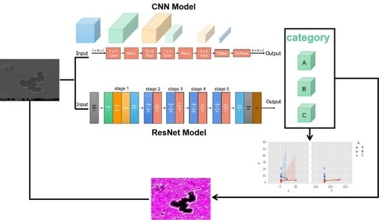
This paper presents a deep learning-based classification model that identifies the bonding strength of Al-Sn-Al and determines the optimal bonding process. The wafer bonding images are processed by CLAHE, dividing the dataset into a training set and a test set based on a 9:1 ratio. After training the CNN and ResNet models in the training dataset, the accuracy of the two is compared in the test dataset. The accuracy of the ResNet model is 99.17%, while the accuracy of the CNN is 91.67%. Thus, the ResNet is much better than CNN. When using the Canny edge detector to identify wafer images, it is found that the wafer fracture pattern is hole-shaped. By calculating the surface area, the smaller the area of hole movement on the wafer surface, the higher the bonding strength. Validation of images of bonding strengths corresponding to different process conditions shows that relatively short bonding times and relatively low bonding temperatures can produce wafers with better bonding quality. The autonomous classification model proposed in this paper enables the identification of images of wafers with different bonding strengths, greatly reducing measurement costs and improving the efficiency of optimizing the bonding process.
2. Experimental and Data Preprocessing
In the present research, we consider the experimental conditions of the literature [
19]. Primarily, 4-inch silicon wafers (thickness of 505–545 μm) are used and a 500 nm-thick aluminum layer is sputtered onto the wafers. Then, a 500 nm-thick tin layer is sputtered onto the aluminum layer resulting in two wafers being stacked in the EVG501 bonder. The wafers are pressed together in a vacuum at a pressure of 0.25 MPa and heated to the bonding temperature. After the bonding is complete, the bonded wafers are removed from the wafer fabricator at 200 °C. The shear strength is then measured with the Dage 4000 series shear machine, and after the shear test, the fractured surface images are examined by SEM.
The image dataset was first processed to improve computer recognition through histogram equalization. Histogram Equalization (HE) [
22] is a transformation method that makes the grayscale histogram distribution of an image more uniform. By taking the grayscale value as the abscissa, and the number of pixels corresponding to the grayscale value as the ordinate, the histogram of the grayscale image is produced. The conversion function
T(
x) is as follows:
For grayscale images, the distribution of x is 0–255, N is the total number of pixels in the image, and nx is the number of points. However, there are some problems with the results obtained by HE transformation. For instance, some areas are noisy due to excessive contrast enhancement, while others are darker/brighter after adjustment. Therefore, detailed information is lost during HE transformation.
As a result, this paper utilizes the contrast-limited adaptive histogram equalization (CLAHE) [
22] algorithm to enhance images, a form of adaptive histogram equalization that uses bilinear interpolation. In the grayscale histogram of the image, the degree of contrast magnification is proportional to the slope of the histogram of the probability distribution of pixels. Therefore, those elements beyond a certain threshold are equally distributed in the rest of the histogram. At the same time, the contrast is limited by restricting the slope of the cumulative distribution function to limit noise amplification.
3. Methods, Results, and Discussion
In this research, the bonding strength classification of wafer bonding images is performed by constructing the CNN and ResNet models. The specific implementation process is as follows. Firstly, images with different bonding strengths were labeled and divided into three possible categories, such as 0–5 MPa for category A (bonding temperature including 280 °C, 330 °C, and 380 °C, bonding time including 3 min and 50 min), 5–10 MPa for category B (bonding temperature including 280 °C, bonding time including 3 min and 20 min), and 10–20 MPa for category C (bonding temperature of 280 °C, bonding time of 3 min). In the images used, the bonding size is in the range of 0–10 μm. Secondly, translation, stretching, and rotation were used to expand the dataset. Then, the training set and the test set were divided using a 9:1 ratio, and the original image was converted using the CLAHE transformation and dataset enhancement. These are then inputted into the 2-layer CNN model and the 50-layer ResNet model to produce accuracy rates for classification. Thirdly, Gaussian filtering [
29] was applied to remove image noise when analyzing wafer surface morphology using the Canny edge detector. The edge contour was identified, and the area was calculated based on the resultant change in image pixel intensity. The model training and testing environment was the Windows 10 system, 2.3 GHz Intel Core (TM) i7-11800H GPU, 16.0 GB memory, 3050Ti graphics card, Python language, Pytorch, TensorFlow, and Keras architectures.
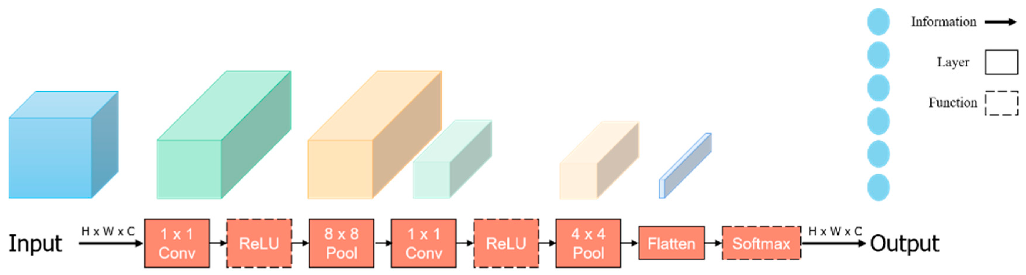
3.1. CNN Model
The main links in CNN models are the convolutional layer, the pooling layer, and the fully connected layer. When an image is inputted into the convolutional layer, the application deviation and the nonlinear function (ReLU) [
30] can output a new dimension image (Equation (3)). As the convolutional layer uses parameter sharing and sparse connection, it can effectively reduce the neural network parameters and prevent overfitting. In addition to the convolutional layer, CNN often utilizes maximum pooling to improve features’ calculation speed and robustness, reducing the model’s size. When
in Equation (3) is set to zero, the output image dimension can be calculated after the pooling layer. Finally, the output from the previous layer is flattened into a one-dimensional vector, and then a new layer is constructed according to the weights and deviations. The elements in the new layer are closely connected with the elements in the one-dimensional vector layer to form a fully connected layer.
where
is the size of the input image,
is the number of the Padding,
is the size of the filter, and
is the stride.
This experiment established a two-layer CNN image classification architecture (
Figure 1), trained through the training set, and then tested on the test set. The exact steps are as follows:
Initialize the model parameters using random initialization.
Set the stride of the convolutional layers to 1, and padding to “same”.
Choose ReLU as the activation function.
Set the pooling layers filters to 8 × 8 and 4 × 4, and padding to “same”.
Check the model by calculating the cross-entropy loss.
Use Adam to optimize the model.
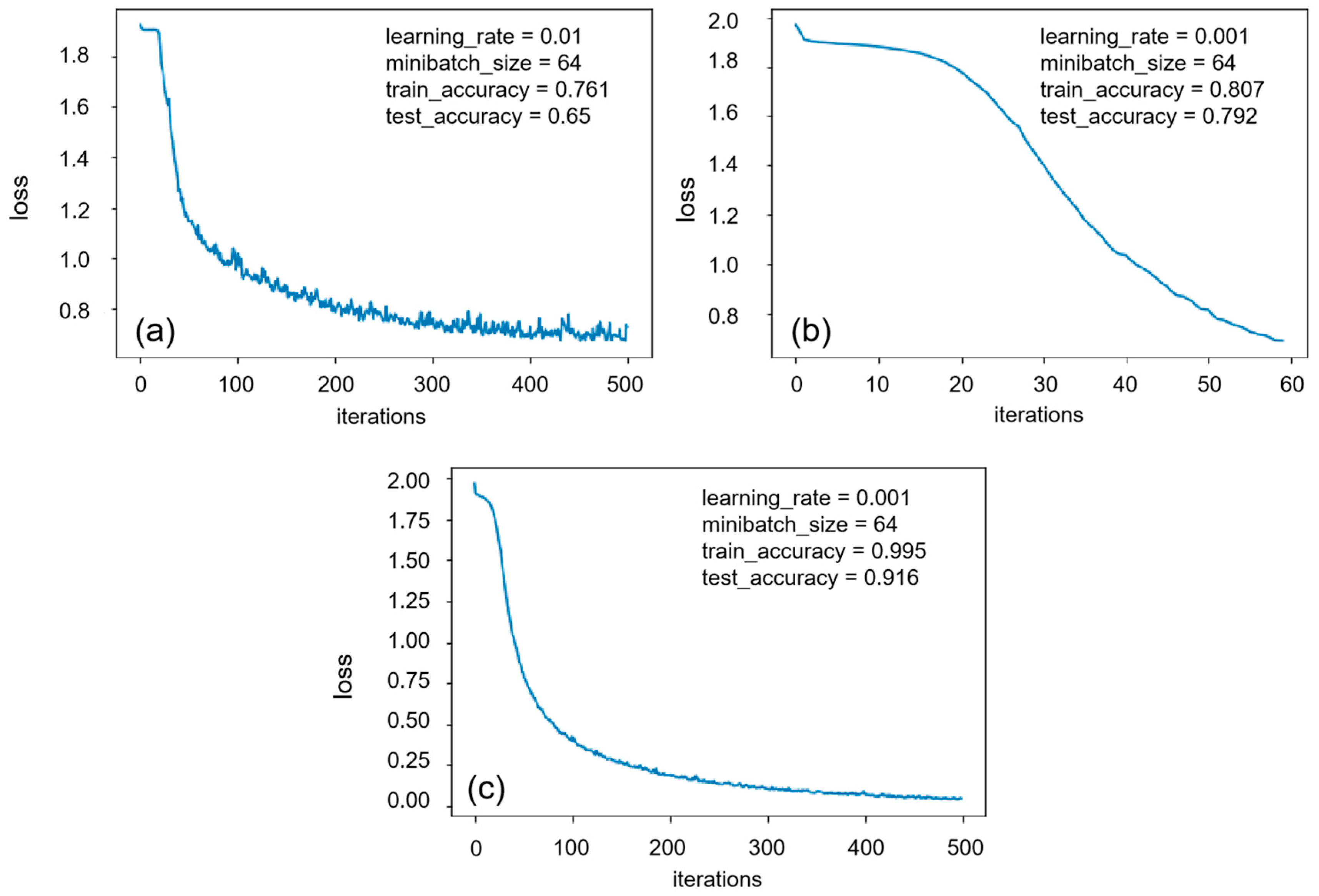
As shown in
Figure 2, compared to the three sets of parameters. When the learning rate and iteration were set to 0.01 and 64, respectively, the accuracy rates of the model for the training set and test set were 76.11% and 65%, respectively (
Figure 2a).When the learning rate and iteration were set to 0.001 and 64, respectively, the accuracy rates of the model for the training set and test set were 80.74% and 79.17%, respectively (
Figure 2b).As the learning rate and iteration were set to 0.001 and 500, respectively, the best accuracy rates of the model for the training set and test set were 99.54% and 91.67%, respectively (
Figure 2c).
3.2. ResNet Model
When the network continues to deepen, the deep ordinary network is less capable of selecting the parameters of the learning identity function, resulting in a series of degradation problems, such as gradient disappearance and gradient explosion. Therefore, addressing degradation problems by introducing a ResNet model is an efficient method, which can form a deep neural network by stacking residual blocks.
As shown in
Figure 3, each two layers added a shortcut connection to form a residual block, with multiple residual blocks forming one residual network. The core of ResNet is the residual block, which is defined as
; where
and
are the input and output of the
l-th residual unit, respectively;
is the activation function;
is the residual function; and
is the convolution kernel. The residual network [
16] uses the original input information to transmit directly to the following layers and avoid accuracy rising and then plateauing as a result of an excessive number of convolutional layers. Assuming that the input to a particular neural network is
, and the expected output after convolution pooling is
, then the goal of learning is
. Moreover, in the ResNet model, the input
is directly passed to the output, and the learning goal is
, which is the residual. The input is directly connected to the following layer through the bypass branch so that the last layer can directly learn the residual error, thereby forming a shortcut connection. Based on this structure, a specific network layer provides the activation, which is then quickly fed to another layer, or even a deeper layer consisting of the neural network, for identity mapping. Therefore, the shortcut connection construction can train the ResNet model. In some situations, the depth can exceed 100 layers.
This paper used the ResNet50 network structure for modeling, consisting of 49 Conv layers and one FC layer predicted by SoftMax (
Table 1). The accuracy of the training and test dataset was 100% and 99.17% when the number of iterations and small batches were 100 and 64, respectively. Compared to the ResNet network structure, the CNN model has two distinct advantages—faster operation speed and lower memory consumption. Nevertheless, ResNet performed much better than CNN in terms of result accuracy and number of iterations. Therefore, based on the deep learning approach, CNN and ResNet classification recognition models were constructed by analyzing the morphology of wafers, and using the models, the range of binding intensity of other wafers could be identified. After comparing the recognition results of the two models, it was found that the accuracy of ResNet was higher than that of CNN.
3.3. Canny Edge Detection
In this paper, the surface area is divided and calculated using the Canny edge detector after the edge in the image has detected the wafer surface morphology as hole-shaped. Canny detection [
31] involves identifying the edge through a change in the image pixel, as the pixel intensity is very high at the edge and low in the internal area. The specific steps in the Canny edge detector process for edge identification are described in the following subsections.
3.3.1. Noise Reduction
When the image has a large amount of random noise, said noise is detected as an edge, which leads to false detection. Therefore, the Gaussian filter is first used to convolve and smooth the image by reducing the influence of noise on the edge detection result.
3.3.2. Gradient Calculation
Since the image edge direction is different, the Canny algorithm uses four operators to detect horizontal, vertical, and diagonal edges in the image. The edge detection operator (such as Roberts, Prewitt, and Sobel) returns the first derivative value of the horizontal
Gx and vertical
Gy directions to determine the gradient and direction of the pixel.
where
is the gradient strength and
is the gradient direction.
3.3.3. Non-Maximum Suppression
The edge of the image extracted only based on the gradient value is still blurred, but non-maximum value suppression can set all gradient values except the local maximum to 0, thereby clearing the image edge. First, the gradient intensity of the current pixel is compared with the two pixels in the positive and negative gradient directions. Second, if the gradient intensity of the current pixel is larger than that of the other two pixels, the pixel remains an edge point. Otherwise, the pixel is suppressed. Thus, the spurious response caused by edge detection can be eliminated.
3.3.4. Double-Threshold Detection
After applying non-maximum suppression, the remaining pixels can more accurately represent the actual edges in the image. However, some edge pixels are caused by noise and color changes. It is necessary to filter out edge pixels with weak gradient values and retain edge pixels with high gradient values. One technique for achieving this is to select high and low thresholds. If the gradient value of the edge pixel is above the high threshold, it is marked as a firm edge pixel. Meanwhile, if the gradient value of the edge pixel is below the high threshold and above the low threshold, it is marked as a weak edge pixel. Finally, if the gradient value of the edge pixel is below the low threshold, it is suppressed.
This paper compares three sets of parameters of the CNN model. According to the data, the best results were obtained when the epoch was 500 and the learning rate was 0.001. The accuracy rates for the training and test sets were 99.54% and 91.67%, respectively (
Table 2). After comparing the three sets of parameters of the ResNet50 model, the output was optimized when the calendar time and batch size were 100 and 64, respectively, with an accuracy of 100% and 99.17% for the training and test sets, respectively (
Table 3).
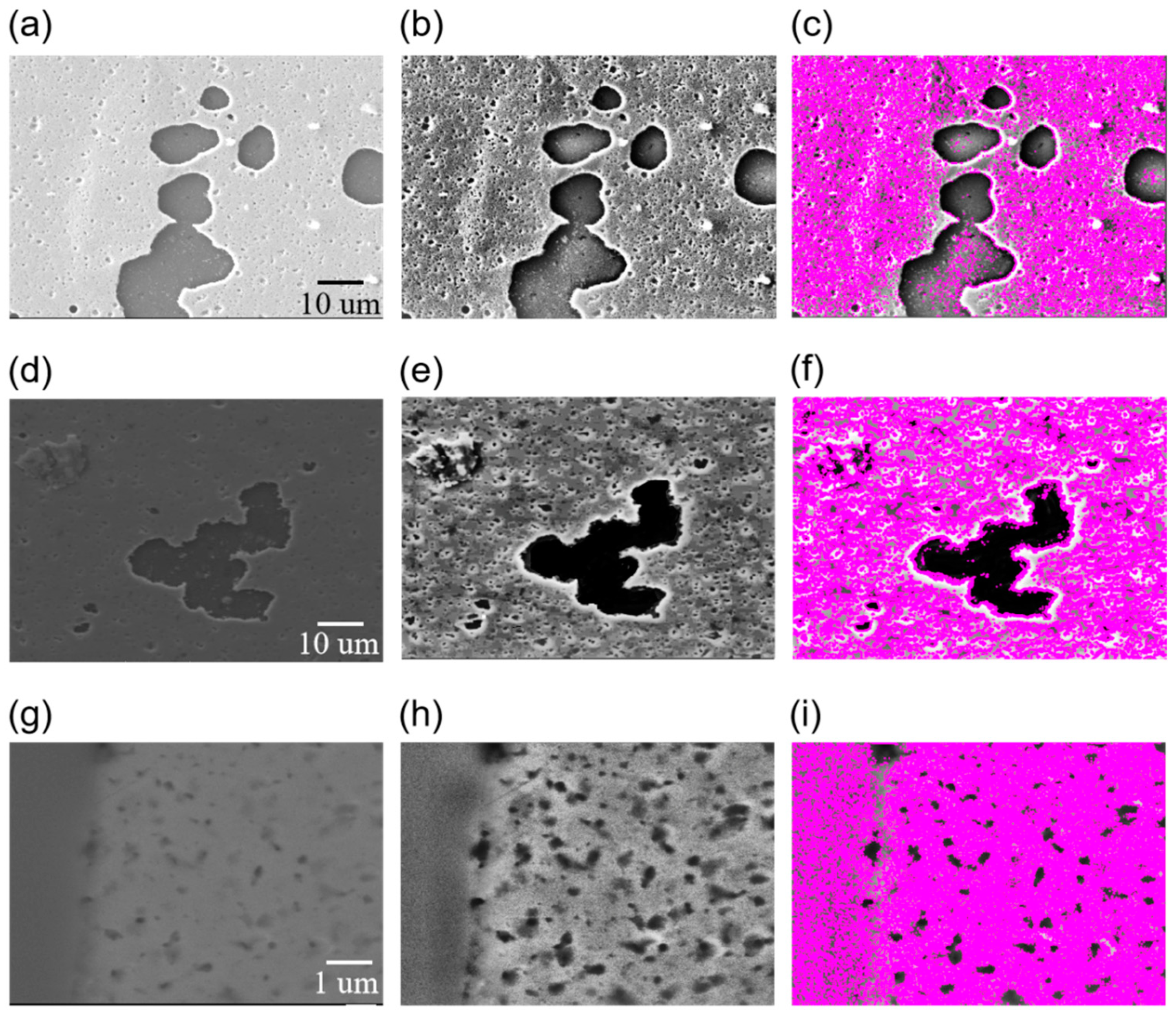
Figure 4 shows the Canny edge detector dividing and calculating the area of Sn on the wafer surface morphology. Here the bonding strength rises from 4.01 Mpa to 12.6 Mpa, while the Sn area on the wafer surface rises from 236 to 5621.5. At the same time, the holes become smaller. As a result, the size of the holes is generally smaller, while the bonding strength is higher. The morphology of the wafer gives a good indication of the quality of the bonding process. When the wafer morphology is formed in the manner shown in
Figure 4, the surface is hole-shaped. In images A, B, and C (after the application of the Canny detector), the area of Sn on the wafer surface increases, and the size of the surface hole decreases as the bonding strength increases. It is well illustrated by the fact that the smaller the area of the hole in the fracture pattern on the wafer surface, the greater the bonding strength (
Table 4). In this case, both the bonding temperature and the bonding time have a particular influence on the bonding strength of the wafers. When the Sn melts at 231 °C, the oxide layer on the Sn surface breaks down under the bonding pressure, and the Sn layers on the upper and lower wafers fuse well together, with the liquid Sn flowing between the Al-covered wafers and the Sn film taking on a porous form. When the bonding time and temperature increase, the Sn film at the bonding interface becomes more porous, and the Sn film gradually loses its ability to connect the upper and lower Al-covered wafers, and the bonding strength becomes significantly smaller. As shown in
Figure 5, wafers with weaker bonding strengths require relatively long bonding times and relatively high bonding temperatures. It can be deduced from this that relatively short bonding times and relatively low bonding temperatures can produce wafers with better bonding quality.


