1. Introduction
ZnO is both a piezoelectric and semiconducting material [
1], with an energy band gap of about 3.37 eV. A broad range of applications have been demonstrated for one-dimensional (1D) ZnO nanostructures, for example as a photoconductor [
2], field emitter [
3], logic gate [
4], and waveguide [
5]. Recently, the application of ZnO nanowires in energy conversion, for example in dye sensitized solar cells [
6] and gas sensors [
7], has attracted increasing research interests. These developments have as a goal to conserve and extract energy from the environment by exploring the physical properties of ZnO nanostructures.
In recent years, ZnO nanowire (NW) array based nanogenerators (NGs) have shown great potential to convert mechanical to electrical energy by using the coupling effects of the semiconducting and piezoelectric properties of ZnO [
1,
8,
9]. However, to acquire sufficient piezoelectric NG performance for practical applications, further developments of ZnO NWs for mass production require full control of the synthesis process and nanowire morphology, as well as their crystal quality.
Currently, there are numerous methods to grow ZnO NWs, such as vapor-liquid-solid processes (VLS) [
10], metal-organic chemical vapor deposition (MOCVD) [
11], or thermal evaporation methods [
12].
However, these processes require high pressures and temperatures, as well as acid-resistant environments, which makes them difficult to integrate with standard fabrication methods and future flexible electronics. Thus, new green approaches are crucial for the development of novel nanostructures. Recent solution methods for the synthesis of ZnO NWs have been engaged because of their low growth temperatures, low cost, and the potential for scaling up. Additionally, low temperature solution based growth techniques have been investigated for the formation of ZnO NWs on the surface of materials such as carbon fibers, tows, or fabrics in order to enhance the interfacial strength, excluding weakening of the composite materials during high temperature processing [
13]. Hydrothermal synthesis has many merits that can allow the production of uniform and well distributed ZnO NW arrays. Moreover, the diversity of materials into which ZnO NWs can be incorporated and on which they can be grown addresses challenges in multiple technological domains, such as the military, with the improvement of Kevlar and composite fabrics [
14], as well as health care and environmental applications with the development of multifunctional wearable sensors [
15]. In this regard, our research group has reported a hydrothermal process for producing arrays of ZnO NWs on conductive substrates below 100 °C [
16,
17,
18,
19,
20,
21,
22].
In addition, the seed layer is very important for the growth of high quality ZnO NWs, and plays a remarkable role in their properties [
18,
23,
24]. As is largely known, to synthesize continuous and well aligned ZnO NWs, it is necessary to use a ZnO seed layer.
Many authors have reported the effect of ZnO seed layer with different thicknesses on the growth of ZnO NWs [
23,
24,
25,
26]. These reports showed thicknesses ranging from 20 to 1000 nm, all of which influence the alignment of ZnO NWs; parameters which affect the alignment are not entirely known yet, and the study of such parameters still remains a challenging issue for the scientific community. In particular, it is suggested that the enhancement of the surface condition and the interfacial properties of ZnO NWs are key factors in determining nanodevice performance through the creation of a functional gradient between the NWs and matrix, which has been shown to improve load transfer [
18,
27,
28]. Besides the seed layer thickness effect on the growth of NWs, there is an effective method to modify the surface condition of ZnO NWs, which consists of thermal annealing of the ZnO seed layer. In particular, the annealing treatment improves the crystallinity of the ZnO seed layer and the adhesion on the substrate, which contributes to well-aligned ZnO NWs and could consequently have a significant effect on piezoelectric nanogenerators.
The present work reports the growth of ZnO NWs on a ZnO seed layer by hydrothermal synthesis method. The influences of deposition time and annealing treatment of the ZnO seed layer on the ZnO NWs were studied.
2. Experimental Details
The substrate cleaning was carried out with hydrofluoric acid HF (50%), hydrogen peroxide H2O2 (30%), and sulfuric acid H2SO4 (96%), which were supplied by KMG ULTRA PURE CHEMICALS SAS (Saint Fromond, France), and all of which were used without further purification. The chemicals used for the ZnO NW growth included zinc nitrate hexahydrate Zn(NO3)2∙6H2O (98%), hexamethylenetetramine (HMTA) (CH2)6N4 (>99,5%) purchased from Sigma-Aldrich S.a.r.l (Saint-Quentin Fallavier, France), and ammonium hydroxide NH4OH (29%) solution from KMG ULTRA PURE CHEMICALS SAS (Saint Fromond, France), also used as received. The deposition of metallic layer was done with physical vapor deposition (PVD) equipment (Plassys MP 650 S, Marolles-en-Hurepoix, France), and the ZnO seed layer deposition with a PVD equipment (Plassys MP 550 S, Marolles-en-Hurepoix, France). By offering the opportunity to work on small as well as large substrate areas up to 8 inches, this PVD equipment underlines the scale–up potential and industrial interest of the fabrication processes described in the following section. A tubular furnace (Thermolyne 79300, Dubuque, IA, USA) was used for the ZnO seed layer annealing treatment. A stainless steel temperature controllable autoclave (Parr Instrument Company, Moline, IL, USA) was used to operate the synthesis of ZnO NWs.
The entire study was performed using
n-type, 500 µm thick silicon wafer (100) cut into 2 × 2 cm² samples. The standard cleaning procedure [
29] consists of first immersing the substrates in a bath of a mixture of sulfuric acid and hydrogen peroxide (H
2SO
4:H
2O
2, 1:1) for 10 min at 110 °C, in order to remove any metallic and organic contaminants, followed by a rinse session in deionised (DI) water. Secondly, they are cleaned for 2 min in diluted hydrofluoric acid (25 %) to remove the native oxide layer of SiO
2 usually formed at the Si surface, before a last rinsing in DI water. Last but not least, the substrates are dried under nitrogen flow.
On the top of the silicon samples, a 100 nm thick adhesive titanium layer was direct current (DC) sputtered by magnetron plasma at 500 Watts and under 5 mTorr pressure in argon atmosphere. A 200 nm gold layer was added following the same protocol, to serve as bottom electrode for the future nanogenerator applications. As is well known, the titanium layer improves the interfacial bonding by reducing the lattice mismatch between the silicon (100) and gold (111) layers [
30].
Last, a ZnO seed layer was radio-frequency sputtered on the gold surface (65 W, 5 mTorr) under an argon atmosphere. Several deposition times were set to deposit the ZnO seed layer, corresponding to 100, 50, 10, and 5 nm thicknesses and checked by profilometer (KLA Tencor, Milpitas CA, USA). The aim of the seed layer is to promote the heterogeneous growth of ZnO NWs on the substrate, and to help control their crystallinity as well as their orientation [
25,
31,
32]. Next, to study the influence of annealed seed layers on the morphology and alignment of ZnO NWs, a thermal treatment was performed at 400 °C for 30 min in air through a horizontal quartz tubular furnace. A summary of the various conditions is presented in
Table 1.
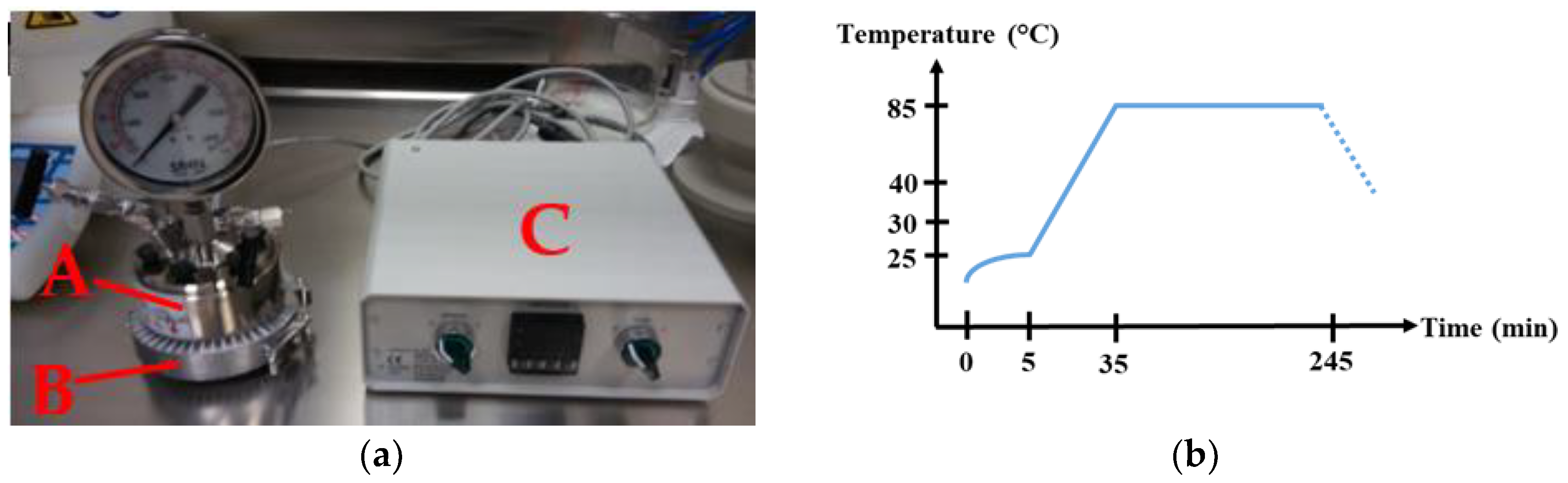
The hydrothermal synthesis of ZnO NWs on ZnO seed layer coated substrates was carried out in the 150 mL stainless steel temperature controllable autoclave shown
Figure 1a. The temperature regulation was set with a ring heating system wrapping the external wall of the autoclave. This system gives the advantage of an efficient conduction of the heat into the growth solution, due to the direct contact between the ring and the metallic reactor and thus reduces the growth time in comparison to a reactor placed in an oven. In addition, the ring heating system wraps the entire lateral volume of the growth solution in order to provide a good homogeneity of temperature in the medium. In that way, this ring heating system tends to be a good approach of the chemical industrial synthesis conditions that use double wall reactors to heat up large volumes of solutions.
Two clear and transparent fresh stock solutions of Zn(NO
3)
2 and HMTA (100 mM) were separately prepared in DI water, as well as an ammonia solution (30 mM) by dilution of NH
4OH (29%). To hydrothermally grow the ZnO NWs, the autoclave was filled with the solutions following this order: zinc nitrate hexahydrate (34 mM), HMTA (34 mM), and ammonia (0.8 mM) before stirring. The pH of the obtained colorless growth solution is known to be around 7.4. The substrates were tilted against the walls to prevent the precipitation of homogenous nucleated ZnO on the seed layer surface. After hermetically sealing the autoclave in order to avoid evaporation, the system was heated up to 85 °C for 4 h, including a 30 min ramp of temperature following the path shown in
Figure 1b. The real temperature reached by the growth solution inside was actually about 70 °C.
The mechanisms involved during the ZnO NW formation on the ZnO seed layer can be summarized by the following equations:
The role of HMTA in ZnO hydrothermal synthesis is to date a subject of argument within the scientific community. However, the main experiments and interpretations raised by researchers present HMTA as a reactant with a dual behavior in the solution. First, besides acting as a pH buffer, HMTA becomes a provider of hydroxyl ions OH
– when it is slowly decomposed into ammonia and formaldehyde following Equation (1). This ammonia formation will provide both ammonium ions and hydroxyl ions for ZnO formation (Equation (2)) [
33,
34].
Secondly, HMTA is also suspected to act as a capping agent to promote the anisotropic growth of ZnO in the (002) direction. By preferential attachment to the non-polar facets of the nanowire [
35,
36,
37], HMTA induces steric hindrance effects to prevent the lateral growth of the nanowire.
The mechanisms surrounding the zinc species start with the hydrolysis of the zinc salt which releases Zn
2+ ions. They will later form a complex [Zn(H
2O)
6]
2+, with water molecules free to react with OH
– to form different monomeric hydroxyl species such as Zn(OH)
2(aq), Zn(OH)
2(s), and Zn(OH)
+(aq) (Equation (3)–(5)), mainly present in near neutral conditions [
18,
38,
39]. ZnO is then obtained by condensation of those different species (Equation (6)). As all these reactions are occurring in equilibrium, Zn
2+ ions can also form the [Zn(NH
3)
4]
2+ complex (Equation (7)). In that case, by acting as a complexing agent, NH
3 helps to regulate the fast consumption of Zn (II) ions by homogeneous nucleation.
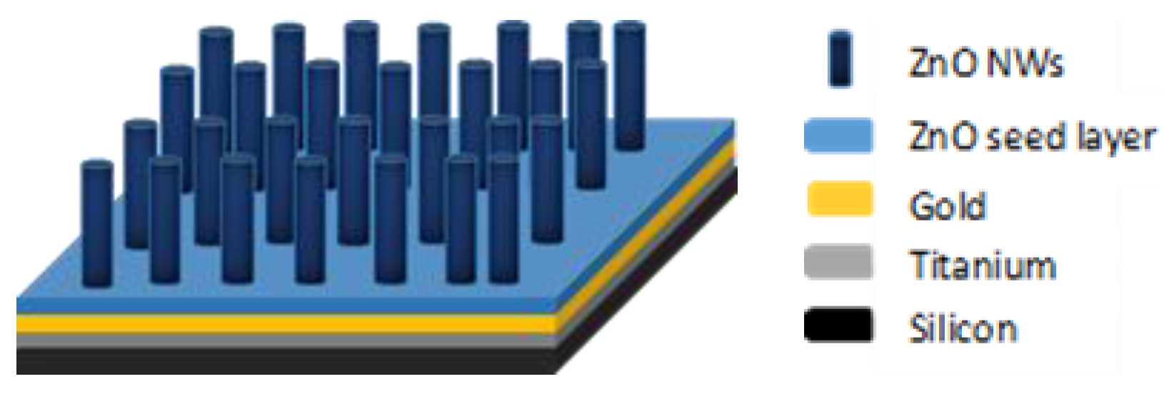
After the growth, the samples were taken out, rinsed by spraying deionised (DI) water, and finally dried under air flow. The structure of the samples obtained after hydrothermal growth is given in
Figure 2.
Structural characterizations of the ZnO seed layer and NWs were performed using X-ray diffraction (XRD) with a CuK1 radiation on the high-resolution parallel beam diffractometer (Bruker AXS D8 discover, Karlsruhe, Germary). The morphological characterizations of the ZnO NW surfaces and cross sections were done by high resolution transmission scanning electron microscope (HRSEM, JEOL JSM-7900 F, Croissy-sur-Seine, France). The extraction of the densities, lengths, and diameters associated with the ZnO NWs was obtained using Image J software on SEM images. The density derived from the number of NWs on each sample was calculated on 15 µm², 8 bit images, with the application of a binary mask and a watershed filter allowing better segmentation of adjacent NWs. With a 4 nm low-cut filter on the particle size analyzed, the accuracy of the count is estimated to be 95%. The roughness of the ZnO seed layers was measured with an Atomic Force Microscope (AFM, Bruker France SAS, Dimension ICON, Palaiseau, France).
3. Results and Discussion
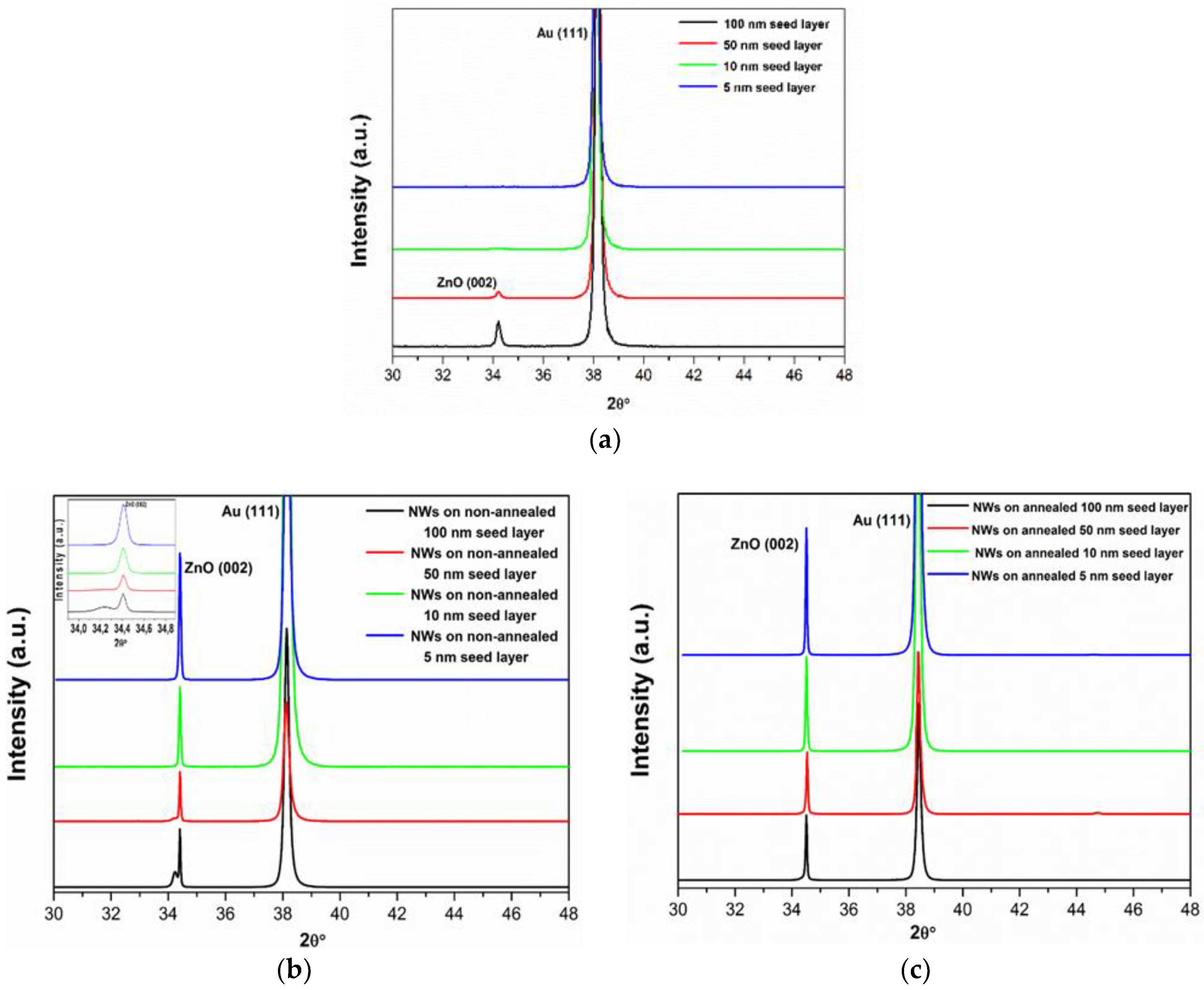
Figure 3a shows the XRD patterns of different thicknesses of ZnO seed layers deposited on Au/Ti/Si and grown by sputtering technique. The X-ray diffraction peaks can be indexed to the hexagonal wurtzite ZnO structure (JCPDS file No 05-0664). As can be seen from the XRD data, with decrease of seed layer thickness, the (002) intensity decreased and the full-width at half-maximum (FWHM) of the (002) diffraction peak increased. Therefore, the crystal size of seed layers decreased with decrease in thickness. The crystal sizes of the ZnO seed layers were calculated using the well-known Scherrer equation (Equation (8)):
where λ, θ, and β are the X-ray wavelength (0.154 nm), Bragg’s diffraction angle, and FWHM of the ZnO (002) diffraction peak, respectively. According to this formula, the crystal sizes of the ZnO seed layers were 52 and 44 nm for the thicknesses of 100 nm and 50 nm, respectively. Regarding the lattice constant
c, it was calculated by the following relationship (Equation (9)) [
40]:
where
h,
k, and
l are crystal Miller indices, and
d is the interplanar spacing, respectively. The lattice constant
c, calculated from the present XRD data for ZnO seed layers, was 5.2613 and 5.2395 Å for the thicknesses of 100 nm and 50 nm, respectively (
c = 5.1876 Å for JCPDS card No. 05-0664).
After that, ZnO NWs were hydrothermally grown on different thicknesses of ZnO seed layers (
Figure 3b). It was observed that the entire sample exhibited the dominant peak at a position corresponding to the c axis (002) orientation, confirming that the nanowires grew predominantly along the [001] direction. However, the (002) peak splitting was seen in the XRD pattern of ZnO NWs grown onto the ZnO seed layer with a thickness of 100 nm. This property may be understood in terms of the effect of the seed layer. The ZnO NW peak splitting was shifted rightwards from the ZnO seed layer substrate peak, suggesting that it has a smaller lattice constant than that of ZnO seed layer. The lattice constant
c was calculated (see Equation (9)) to be 5.1992 Å for ZnO NWs and 5.2613 Å for ZnO seed layer with a thickness of 100 nm, reflecting a large lattice mismatch between NWs and seed layer. The lattice mismatch induced randomly oriented and poorly aligned ZnO NWs. Moreover, we can note that the intensity of the (002) peak systematically increased with the seed layer thickness diminishing, demonstrating that the NWs grew more densely on a ZnO seed layer deposited with lower thickness. This is related to a reduction of the lattice constant
c of the ZnO seed layer, which caused a decrease of lattice mismatch between NWs and seed layer. This result, paralleling with the SEM observation, underlines the strong influence of the ZnO seed layer thickness on the distribution and the density of subsequently grown NWs.
Next, we tested the effect of annealing of the ZnO seed layers, again on a 100 to 5 nm series, on the growth and orientation of ZnO NWs. The XRD patterns of ZnO NWs are shown in
Figure 1c and illustrate that, by annealing the ZnO seed layer, a typical hexagonal c axis (002) orientation was found in all cases. It was observed that the NWs grown on 10 and 5 nm thin ZnO seed layers had a highly oriented [001] direction, which is evidence of the epitaxial growth of ZnO.
Furthermore, the lattice constants c of ZnO NWs grown on thicknesses of 100, 50, 10, and 5 nm, as calculated from the positions of the (002) reflections were 5.1948, 5.1940, 5.1936, and 5.1931, respectively, which is in close agreement to the reported value of 5.1876 Å for a relaxed system (JCPPS card No. 05-0664). Therefore, annealing ZnO seed layers thinner than 50 nm resulted in the growth of vertical NWs with both a uniform orientation and a high density.
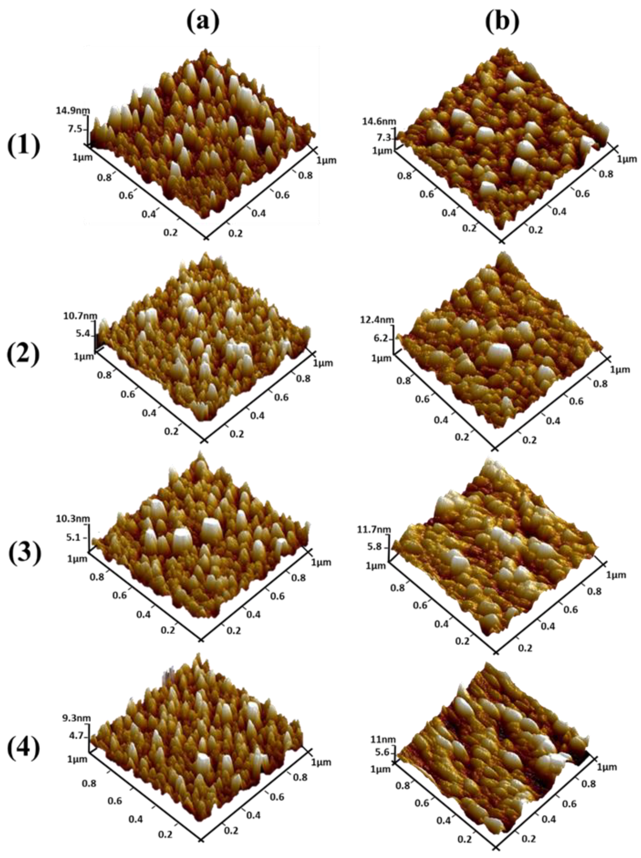
These results confirm that the characteristics of the ZnO NWs are well-shaped c-axis orientation. These characteristics improved due to the use of an annealed ZnO thin seed layer, which was confirmed by SEM images shown in the following figures.
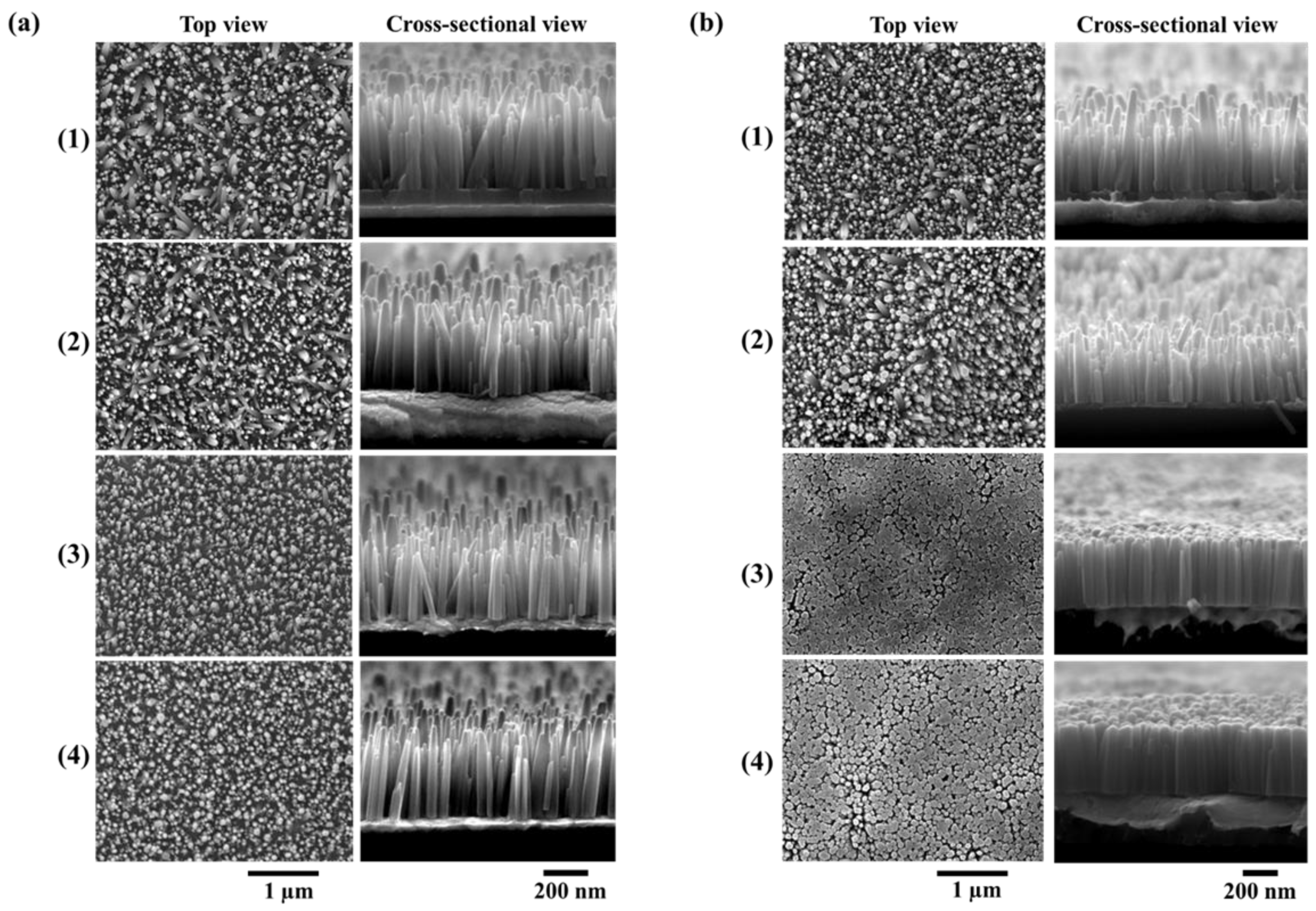
The surface morphology of ZnO NWs grown on non-annealed and annealed ZnO seed layers with different thicknesses is shown in
Figure 4a,b, respectively. It is clear that the NWs growth was strongly influenced by the properties of ZnO seed layers. The NWs with a non-annealed seed layer had different densities (
Table 2), which were estimated by counting the number of NWs from such SEM images using “Image J” software, as mentioned in the experimental section. The NWs density increased significantly with the seed layer thickness decrease, from 35 NWs/µm
2 for the 100 nm sample to nearly 54 NWs/µm
2 for the 5 nm sample, which can be justified by the change in crystal size depending on the seed layer thickness.
The present finding is consistent with previous reports mentioning that the decrease of seed layer thickness causes an increase of nucleation sites on the surface of the seed layer, leading to high NW density [
24,
25]. It can also be seen in the top view and cross section SEM images (
Figure 4a) that the NWs with 10 and 5 nm thin seed layers showed a strong vertical alignment.
As shown in
Figure 4b, the densities of the NWs grown on seed layers annealed at 400 °C increased from 50/µm
2 for the 100 nm sample to 71/µm
2 for the 5 nm sample. It was also seen that the NWs coalesced with other NWs and presented a highly packed vertically aligned structure to form bigger NWs (
Table 2) when the annealing process of the ZnO seed layer was performed, as illustrated in
Figure 4b.4. The thermal annealing process provides sufficient energy to allow the dissociated ZnO atoms to form into a more stable structure, thus resulting in an increase of the nucleation site and an improvement in crystallinity. Meanwhile,
Figure 3c shows a narrower FWHM of XRD (002) orientation for NWs grown on a thinner annealed seed layer, leading the neighbor hexagonal ZnO NWs to coalesce during the synthesis process (
Figure 4b.3–4). Moreover, this phenomenon can be supported by
Figure 4a. Note that poorly aligned ZnO NWs should have no chance to be coalescent. As a result, thinner annealed seed layers with good crystal characteristics make NWs very well aligned.
In addition, the measurement of mean values of diameter d and length L, as well as aspect ratios of the NWs, are reported in
Table 2. Unexpectedly, when looking at the mean values, the decrease of non-annealed seed layer thickness did not seem to significantly impact the diameter nor the length of the NWs. However, the large deviation of length can be attributed to the presence of various shapes of the NWs covering the sample. In fact, this was consistent with the top-view and cross-section SEM images (
Figure 4a.1–2) which show that two distinct populations of ZnO NWs, mainly differentiated by their size, could be found for seed layer thicknesses higher than 50 nm. As the seed layer thicknesses decreased toward 10 and 5 nm, the deviation on the length decreased and the NWs tended to exist under only one type of population (
Figure 4a.3–4).
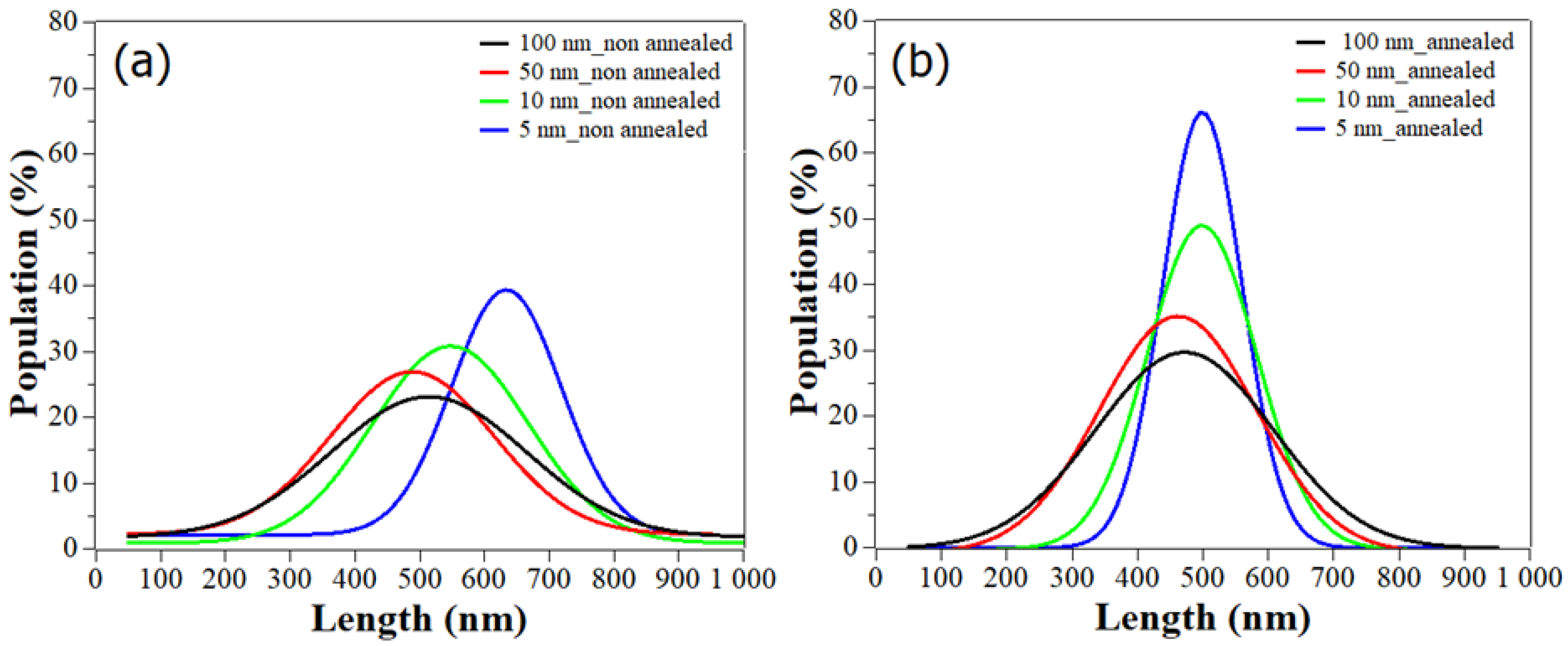
To better understand the influence of the seed layer thickness, and later on the annealing step, on the ZnO NWs length, we plotted the Gaussian fit of the length distribution based on the analysis of NW number (
Figure 5a,b). Given the fact that the seed layer thickness and the annealing step were found to affect the longitudinal direction more significantly compared to the radial one, we chose to only display the distribution profile of the NWs length.
As can be seen in
Figure 5a, when the thickness of the seed layer decreased from 100 to 5 nm, the curves demonstrate, by shifting to the right, a slight increase of length, with peak values corresponding to the predominant length distribution around 510 nm and 633 nm respectively. Additionally, the peak intensity and the FWHM (
Table 3) of the distribution curves are consistent with the SEM images (
Figure 4a), showing a homogenization of the NW population with the decrease of the seed layer thickness. Indeed, for 100 nm thickness, the FWHM value was large: 400 nm, and only 23% of the NWs were centered around 510 nm. This depicts an inhomogeneity in the NW population, which is in contrast to the smaller FWHM value of 216 nm for the 5 nm seed layer, where 39.5% of the NWs could be found around 633 nm. This effect of the seed layer thickness on the morphology and distribution of ZnO NWs can originate from a change in the seed layer structure, and thus in the nucleation mechanism for the ZnO NW growth. In fact, the higher roughness of the thickest seed layers (100 and 50 nm) could promote a grain boundary nucleation mechanism, allowing NWs to grow with less verticality and size homogeneity [
41]. These reports are in agreement with our AFM results, which will be shown later.
As established in the literature, an annealing treatment can improve the structure and surface of a seed layer [
42,
43]. Thus, additionally to its influence on the density of ZnO NWs shown before, we now describe its impact on the diameter and length of the obtained NWs. With the addition of the annealing step, a slight increase of diameter was noticed, as well as a major and global decrease of the NW length. Consequently, a diminution of the aspect ratio was observed from 10 to 6 for the thinner seed layers. This could be due to the limitation by mass transport phenomenon, resulting in the length and diameter of NWs being inversely proportional to the density [
44]. Therefore, due to the annealing treatment leading the increase of the ZnO NW density, a global decrease of the aspect ratio could be expected.
A first glimpse of the improvement of the NW length distribution due to annealing is given in
Table 2. by the smaller deviation values of the length. Especially with 10 and 5 nm seed layer thicknesses, the deviation values decreased from 130 nm to 60 and 40 nm, respectively. The SEM images show an improvement and homogenization of the length distribution for 100 and 50 nm thicknesses (
Figure 4b.1–2)). Furthermore, a clear tendency towards one profile of NWs with equal diameter, length, and alignment was remarkably well depicted by the NWs grown on 10 and 5 nm (
Figure 4b.3–4). Regarding the length distribution shown in
Figure 5b, all the curves shifted toward a central length value of 500 nm. The FWHM values of the Gaussians significantly decreased with the thermal treatment of the seed layers. For small thicknesses, the FWHM was divided by 1.4 (
Table 3), with a percentage of population increasing up to 49 and 66% for 10 and 5 nm, thus showing a trend toward standardization of NW shape. On very thin seed layers, one can note that the ZnO NWs were touching each other due to the high density and alignment. This can be explained by the fact that the annealing treatment did help in rearranging and reducing the grain boundaries of the seed layers, thus promoting a better grain surface nucleation, as previously mentioned.
Hence, in this study, an increase in the NW density was clearly shown with a decrease in the thickness of the seed layers. Moreover, the annealing of thinner seed layers contributed to the formation of vertical well-aligned ZnO NWs with high uniformity.
Figure 6a,b show top view AFM images of ZnO seed layers for the different thicknesses obtained before and after annealing, respectively. One can clearly note that samples exhibit different surface roughness. For the non-annealed seed layers, the average roughness of the 100 nm thick seed layer (
Figure 6a.1) was 2.50 nm and, according to
Figure 4a.1, ZnO NWs grown on this seed layer were not well aligned. Moreover, with a decreasing of the thickness to 50 nm (
Figure 6a.2), the average roughness decreased to 1.73 nm. Finally, when decreasing the seed layer thickness to 10 nm and 5 nm (
Figure 6a.3 and
Figure 6a.4), the average roughness significantly decreased to 1.62 nm and 1.48 nm, respectively (
Table 4). As can be seen, when the surface had minimum roughness, a much better alignment of the NWs was obtained (
Figure 4a.4). The minimum roughness of seed layers promotes less grain boundaries, which should create a switch in the nucleation mechanism of NW growth from poor vertical alignment to well aligned and homogeneous NWs [
41]. As shown in
Figure 6b, the average roughness of the annealed 100, 50, 10, and 5 nm seed layers was 2.86, 2.07, 1.66, and 1.58 nm, respectively, exhibiting a similar trend to the non-annealed seed layers (
Table 4).
The improvement of morphology, alignment, and verticality of the ZnO NWs, due to both the decrease of thickness and the addition of the annealing stage of the ZnO seed layers, allows room for hope when it comes to their integration into our energy harvesting technologies for the improvement of their electrical performances [
45]. However, the coalescence of the NWs can limit the mechanical compression along the c-axis of the NWs [
46] and cause internal screening effects [
47], leading to reduced piezoelectric potential, and thus lower nanogenerator performances.
In order to improve the performances of such systems, it will be interesting to use an annealed ZnO seed layer with a thickness compromise between 50 and 10 nm, which will ensure a good density, uniformity of shape, and alignment of well separated ZnO NWs.

 ,
, 


