Article

Dual-Control-Gate Reconfigurable Ion-Sensitive Field-Effect Transistor with Nickel-Silicide Contacts for Adaptive and High-Sensitivity Chemical Sensing Beyond the Nernst Limit

Department of Electronic Materials Engineering, Kwangwoon University, Gwangun-ro 20, Nowon-gu, Seoul 01897, Republic of Korea
*
Author to whom correspondence should be addressed.
These authors contributed equally to this work.
Chemosensors 2025, 13(8), 281; https://doi.org/10.3390/chemosensors13080281 (registering DOI)
Submission received: 30 May 2025 / Revised: 19 July 2025 / Accepted: 28 July 2025 / Published: 2 August 2025
(This article belongs to the Section Electrochemical Devices and Sensors)

Abstract

In this study, we propose a bidirectional chemical sensor platform based on a reconfigurable ion-sensitive field-effect transistor (R-ISFET) architecture. The device incorporates Ni-silicide Schottky barrier source/drain (S/D) contacts, enabling ambipolar conduction and bidirectional turn-on behavior for both p-type and n-type configurations. Channel polarity is dynamically controlled via the program gate (PG), while the control gate (CG) suppresses leakage current, enhancing operational stability and energy efficiency. A dual-control-gate (DCG) structure enhances capacitive coupling, enabling sensitivity beyond the Nernst limit without external amplification. The extended-gate (EG) architecture physically separates the transistor and sensing regions, improving durability and long-term reliability. Electrical characteristics were evaluated through transfer and output curves, and carrier transport mechanisms were analyzed using band diagrams. Sensor performance—including sensitivity, hysteresis, and drift—was assessed under various pH conditions and external noise up to 5 Vpp (i.e., peak-to-peak voltage). The n-type configuration exhibited high mobility and fast response, while the p-type configuration demonstrated excellent noise immunity and low drift. Both modes showed consistent sensitivity trends, confirming the feasibility of complementary sensing. These results indicate that the proposed R-ISFET sensor enables selective mode switching for high sensitivity and robust operation, offering strong potential for next-generation biosensing and chemical detection.

1. Introduction

The accelerating global aging population, rise in chronic diseases, and advances in personalized medicine have boosted the demand for biosensor technologies capable of real-time, accurate detection, and analysis of biosignals [1,2,3]. For early diagnosis and continuous feedback on therapeutic responses, which are critical for improving patient outcomes, sensors operating reliably in complex and dynamically changing biological environments are required [4,5]. Traditional hospital-centered diagnostic systems cannot meet these evolving demands. Point-of-care (PoC) biosensors—which offer real-time, in vivo monitoring with high mobility—have emerged as the cornerstone of next-generation medical technologies [6,7,8].
Among the various electronic biosensor platforms explored to date [9,10], field-effect transistor (FET)-based sensors have attracted considerable interest owing to their high sensitivity, facile miniaturization feature, and ability to cause direct transduction of chemical signals into electrical outputs [11,12,13,14]. Ion-sensitive field-effect transistors (ISFETs) have been extensively investigated as promising candidates for PoC applications, owing to their label-free detection capability, rapid response, and compatibility with CMOS fabrication processes [15,16,17]. However, conventional ISFETs exhibit intrinsic limitations, such as the Nernst sensitivity limit (~59.14 mV/pH at room temperature) and fixed unipolar conduction modes, which restrict their adaptability to diverse sensing conditions [18,19,20]. For example, n-type FETs offer high carrier mobility and fast response, whereas p-type FETs exhibit low electrical noise and improved signal stability for precision measurements [21,22,23]. Therefore, developing a structurally reconfigurable sensing architecture that can dynamically exploit the advantages of both polarities based on application requirements is desirable.
To address these challenges, we propose a reconfigurable ion-sensitive field-effect transistor (R-ISFET) employing mid-gap Ni-silicide Schottky barrier source/drain (S/D) contacts and a dual-gate control scheme. The device enables dynamic polarity switching between n-type and p-type configurations through the coordinated operation of a control gate (CG) and program gate (PG). The CG governs the potential within the central channel to modulate carrier transport, whereas the PG electrostatically adjusts the band profile near the S/D contacts, regulating carrier injection [24,25]. This design enables real-time mode switching without chemical doping, improving operational flexibility, energy efficiency, and long-term reliability. A dual-control-gate (DCG) configuration enhances capacitive coupling, allowing the device to achieve sensitivity beyond the Nernst limit without requiring external amplification circuitry [26,27,28]. This amplification mechanism has also been reported in applications beyond pH ions, including the detection of low charge analytes such as protein biomarkers [29,30,31,32,33]. An extended-gate (EG) structure is also incorporated to physically decouple the transistor and sensing regions, and thus enhance chemical robustness and device reusability. This EG configuration allows the development of disposable or replaceable sensor systems for diverse applications [34,35,36].
The fabricated device was characterized through electrical measurements (transfer and output curves), and the underlying carrier transport mechanisms in both n-type and p-type configurations were analyzed via energy band diagrams. Sensor performance was quantitatively evaluated via measurement of sensitivity, hysteresis, and drift under varying pH levels, external noise up to 5 Vpp (Vpp denotes peak-to-peak voltage), and interference-prone conditions. The n-type configuration exhibited fast response and high current output owing to its high mobility, whereas the p-type configuration demonstrated minimal drift and hysteresis, maintaining stable operation even under significant external noise. These experimental results validate the feasibility of complementary sensing within a single device, wherein the two configurations adaptively compensate for each other under varying environmental conditions.
The R-ISFET sensor demonstrates that dynamic mode selection enables high sensitivity and robust, long-term operation. These attributes underscore its potential as a versatile and reliable biosensor platform for PoC diagnostics and in vivo monitoring applications.

2. Materials and Methods

2.1. Materials

A p-type silicon-on-insulator (SOI) wafer, featuring a 200 nm buried oxide (BOX) layer and 50 nm top p-type silicon layer with (100) crystallographic orientation, was used as the substrate. Nickel pellets (purity >99%; TFN, Seoul, Korea) and aluminum pellets (purity >99%; TFN, Seoul, Korea) were used for metal deposition. The EG substrate was fabricated using 7059 glass (Corning Inc., Corning, NY, USA). An Ag/AgCl reference electrode (Horiba 2080A-06T; Kyoto, Japan) was used to apply the gate bias. Sylgard 184 polydimethylsiloxane (PDMS) elastomer (Dow Corning, Midland, MI, USA) was utilized to fabricate the fluidic reservoir. The electrode has a glass body with a diameter of 8 mm and a length of 120 mm, filled with a KCl/AgCl internal solution, and was immersed in 100 μL of pH buffer solution within the PDMS chamber during measurements. pH buffer solutions were procured from Samchun Chemical (Pyeongtaek, Republic of Korea).

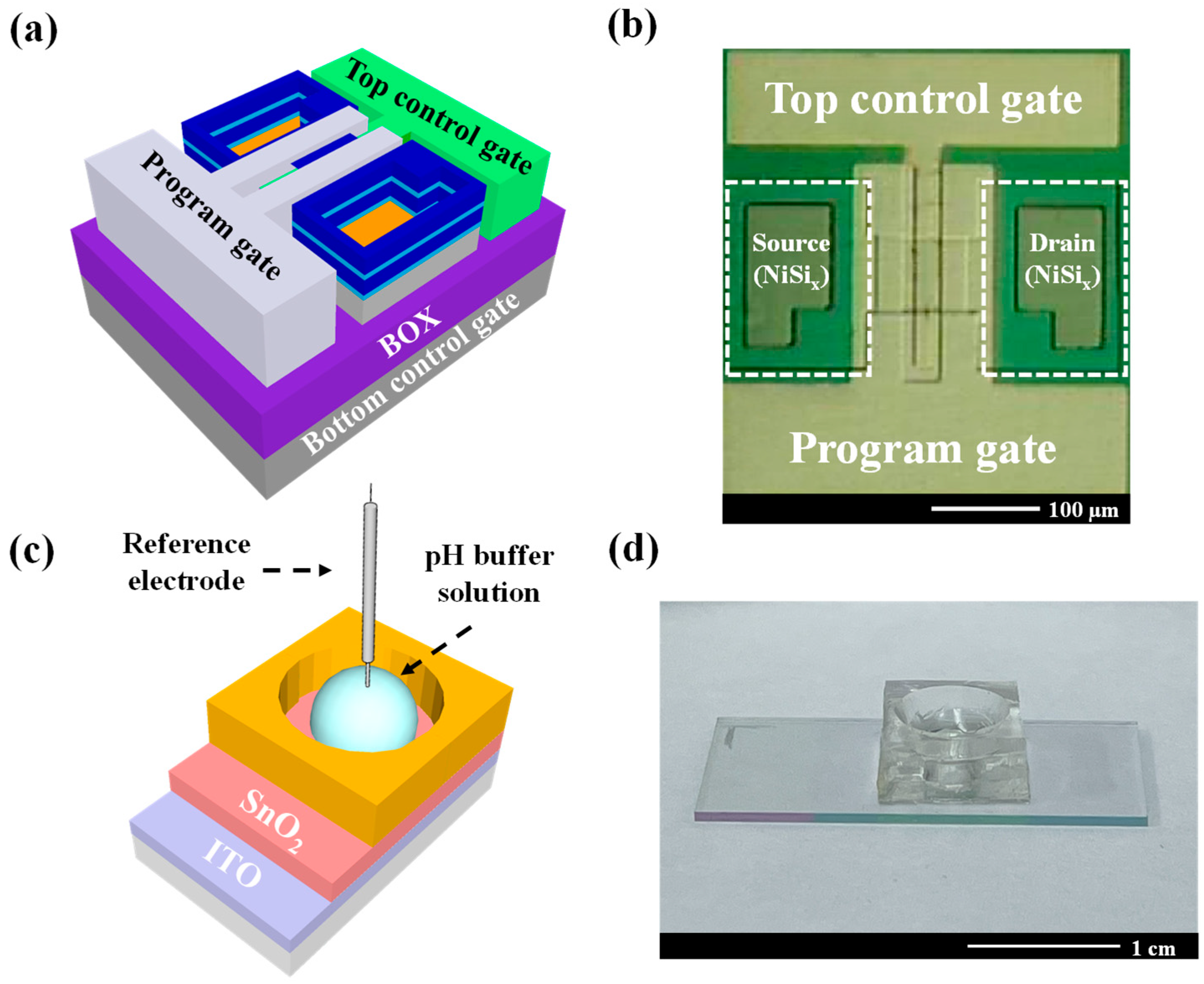
2.2. Fabrication of R-ISFET Transducer Unit and SnO2-Based EG-Sensing Membrane

A 1 × 1 cm2 piece of the SOI wafer was cleaned using the standard Radio Corporation of America process. The active regions, including the channel and S/D areas, were defined by photolithography, and then, the top silicon layer was selectively etched using a mixed acid solution composed of HNO3, H2O, and 49% HF (in a volume ratio of 100:40:3). The resulting R-ISFET transducer featured a channel width and length of 50 and 100 μm, respectively. A 30 nm Ni layer was deposited on the S/D regions via electron beam evaporation and patterned using a lift-off process. Ni-silicide Schottky junctions were formed by microwave annealing (MWA) at 600 W for 2 min in a nitrogen atmosphere. The CG oxide stack was formed by sequential deposition of 20 nm SiO2 and 80 nm Ta2O5 using the radiofrequency (RF) magnetron sputtering method. After defining the CG electrode region via photolithography, an 80 nm Al layer was deposited by electron beam evaporation and patterned by lift-off. The PG oxide was fabricated through two consecutive deposition steps of oxide layers identical to the CG stack. The PG electrode was also patterned by lift-off after depositing an 80 nm Al layer via electron beam evaporation. S/D contact holes were opened by reactive ion etching and subsequently gas annealing (5% H2 in 95% N2) was conducted at 450 °C for 30 min to improve the electrical characteristics of the R-ISFET. Figure 1a presents a 3D schematic of the stacked gate architecture, and Figure 1b shows an optical microscopy image of the fabricated device. Detailed fabrication steps are provided in Figure S1.
The EG sensing unit was fabricated by sequentially depositing a 30 nm thick indium–tin oxide conductive layer and 50 nm thick SnO2 sensing membrane on a 1.5 × 3 cm2 glass substrate via RF magnetron sputtering. The SnO2 layer served as a receptor that transduced surface potential variations, induced by interactions with pH buffer solutions, into electrical signals that were transmitted to the underlying electrode. A PDMS-based fluidic reservoir was mounted on top of the sensing membrane to hold the pH solution. Figure 1c illustrates a schematic of the EG sensing architecture, and Figure 1d displays a photograph of the fabricated sensing unit.

2.3. Device Characteristics

The electrical performance of the EG-unit-integrated R-ISFET was evaluated using an Agilent 4156B precision semiconductor parameter analyzer. All the measurements were conducted in a dark box to eliminate interference due to external light and electrical noise. The crystalline structure of the Ni-silicide layer, formed by MWA, was characterized by X-ray diffraction (XRD; SmartLab diffractometer, Rigaku Co., Tokyo, Japan). The EG sensing unit was electrically connected to the R-ISFET transducer using RG58A 9222 coaxial cables (BELDEN, St. Louis, MO, USA). The Ag/AgCl reference electrode was immersed in the pH buffer solution contained in the PDMS reservoir atop the EG unit and electrically connected to the CG of the R-ISFET. To evaluate noise tolerance, external electrical noise was generated using a DG972 arbitrary function generator (RIGOL Corp., Beaverton, OR, USA) and introduced through the reference electrode.

3. Results and Discussion

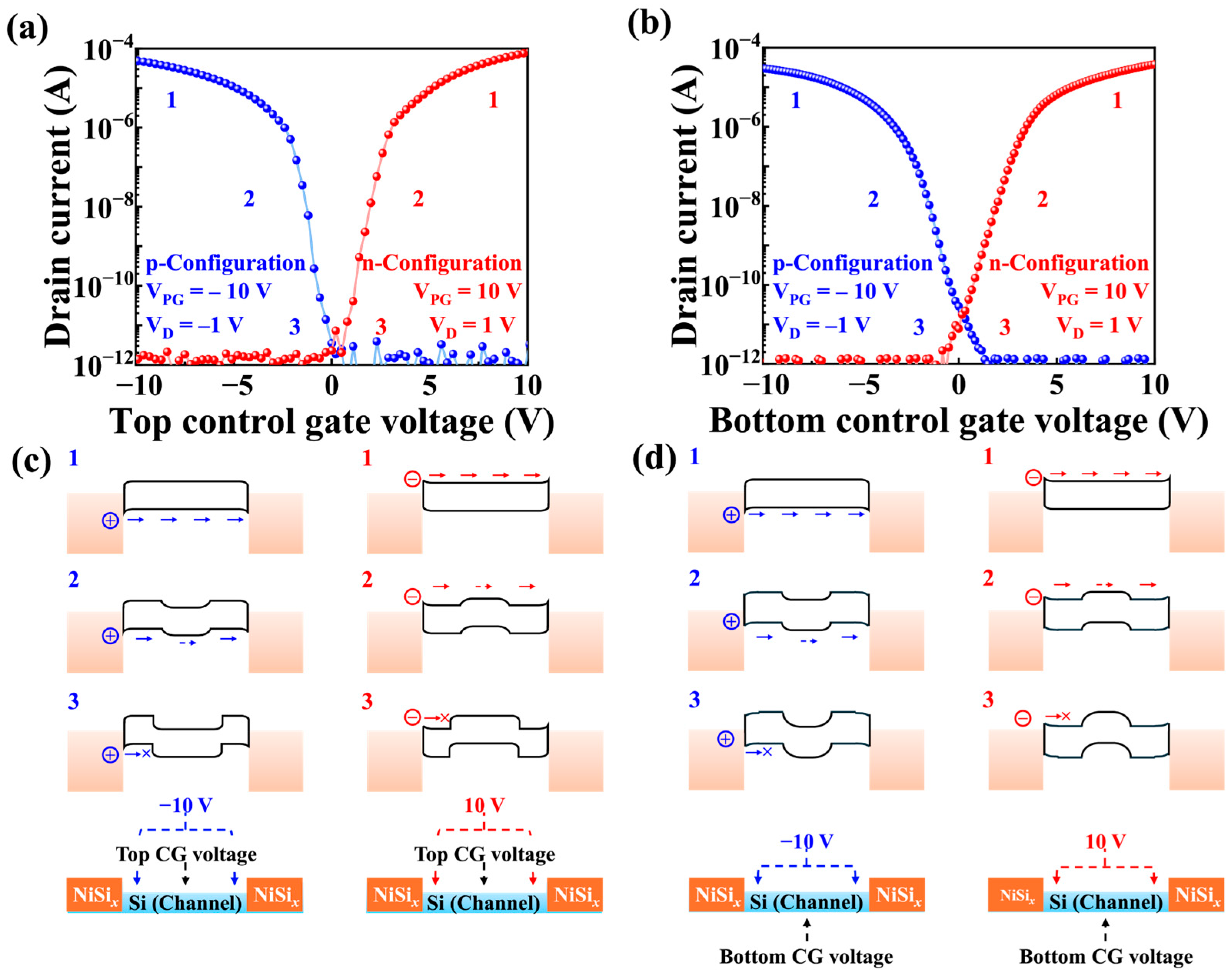
3.1. Characterization of Ni-Silicide S/D for Ambipolar Conduction

Ni-silicide exhibits superior interfacial stability and low contact resistance versus metal–silicon junctions, owing to its ability to form Schottky barriers [37,38]. As a mid-gap silicide, it is advantageous for ambipolar operation in transistor S/D regions [39,40]. To verify Ni-silicide formation and crystallographic quality, Ni was deposited on a p-type silicon substrate, and XRD analysis was performed on as-deposited and annealed samples. To assess electrical properties, sheet resistance (Rs) was measured across three samples: bare p-type silicon, as-deposited Ni, and Ni-silicide formed via MWA. Additionally, the rectifying behavior of Ni-silicide Schottky diodes on p-type silicon was evaluated to confirm the Schottky junction’s performance.
Figure 2a presents the Rs values after sequential processing. The bare p-type silicon exhibited a high Rs of 3.4 × 10⁶ Ω/□. After Ni deposition, Rs dropped to 28.01 Ω/□ and further decreased to 6.02 Ω/□ after MWA, indicating successful silicide formation with markedly reduced contact resistance. The variation in sheet resistance with respect to MWA power is presented in Figure S3a.
Figure 2b shows the XRD patterns of the Ni layer before and after MWA. The as-deposited Ni film exhibited weak, broad peaks at (111) and (200) planes, indicating poorly crystallized Ni. The annealed sample displayed sharp diffraction peaks at (200), (210), (211), (220), (310), and (221) planes, confirming high-quality Ni-silicide formation [41,42]. These distinct peaks indicated that MWA effectively induced a solid-state reaction between Ni and Si, resulting in the formation of a stable silicide structure.
Figure 2c illustrates the current–voltage (I–V) characteristics of the Schottky diode before and after silicidation. The as-deposited Ni contact exhibited weak rectifying behavior with low forward current and high reverse leakage, likely due to interfacial defects and poor junction quality [23]. In contrast, the MWA-processed diode demonstrated distinct rectification, with steep forward current onset and suppressed reverse leakage. The I–V curves corresponding to different MWA power levels are presented in Figure S3b. These results confirmed that 600 W MWA promotes efficient Ni-silicide formation and improves the electrical interface, enabling reliable low-resistance Schottky contacts for ambipolar transistor applications. To obtain the SBH, we used a device area of 320 μm × 230 μm and extracted the reverse current at −2 V from the I to V curves. The calculated SBH was 0.538 eV for the as-deposited Ni/p-Si Schottky diode and 0.634 eV after MWA processing at 600 W.

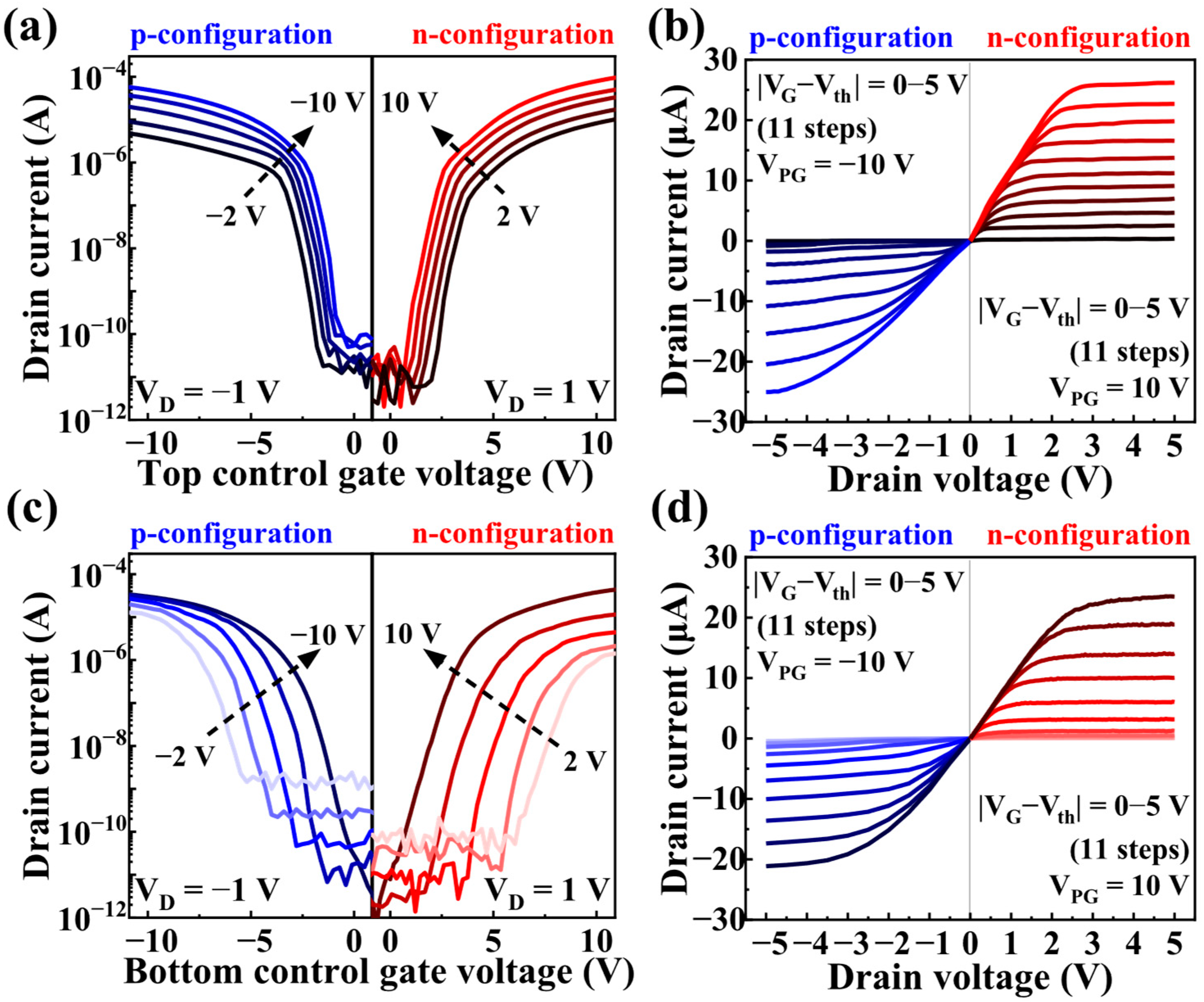
3.2. Electrical Characteristics of R-ISFET with Dynamic Reconfigurability

The transfer characteristics of the fabricated R-ISFET under single top CG operation are shown in Figure 3a. When PG voltage (VPG) is fixed at −10 V, corresponding to p-type configuration, the drain current (ID) increases as the top CG voltage becomes more negative, saturating beyond a threshold. Under a positive VPG of +10 V, indicating n-type configuration, a positive sweep of top CG voltage leads to a sharp increase in ID, demonstrating switching capability between p- and n-type configurations.
Figure 3b shows the transfer characteristics under single bottom CG operation, exhibiting reconfigurable behavior between p-type and n-type configurations, similar to that observed with the top CG. However, the underlying physical mechanisms of gate control differ between the two configurations, as elucidated in the energy band diagrams in Figure 3c,d.
In top CG operation, as shown in Figure 3c, the PG near the source/drain–channel interface enables direct modulation of energy bands in the silicon region adjacent to Ni-silicide S/D, controlling carrier injection. The top CG enhances electrostatic control. A positive VPG pulls down conduction and valence band edges, facilitating electron injection for n-type conduction. A negative VPG raises band edges, allowing hole injection for p-type conduction. The strong band modulation by top CG enables efficient switching due to precise electrostatic control [43].
In contrast, bottom CG operation as shown in Figure 3d features a gate spanning the entire backside of the channel. Though it overlaps the full channel region, its electrostatic control over carrier injection is limited by the low series capacitance of the 200 nm BOX layer. This limitation is quantitatively described by the series capacitance equation [44]:
  1 C =   i t i ε 0 ε r , i
where C is the areal capacitance, ε0 is the vacuum permittivity, εr,i is the relative permittivity, and ti is the thickness of the i-th dielectric layer. According to this relation, thinner layers and materials with higher dielectric constants yield higher capacitance.
In the current device, the bottom CG consists of a single 200 nm SiO2 layer, yielding a low capacitance of approximately 0.173 μF/cm2. The PG stack comprises a bilayer dielectric structure—20 nm SiO2 and 80 nm Ta2O5—sequentially deposited twice, providing a higher effective capacitance of approximately 0.532 μF/cm2. This capacitance difference enables the PG to induce a stronger electric field at the S/D junctions, offering more effective modulation of the local energy bands. Although the bottom CG covers the entire channel, the PG primarily determines polarity switching and carrier injection. These findings highlight the importance of the gate-stack design in realizing reliable and dynamically reconfigurable FET (RFET) operation.
Table 1 summarizes the key electrical parameters extracted from the transfer characteristics, including threshold voltage (VTH), on/off current ratio (Ion/off), field-effect mobility (μFE), and subthreshold swing (SS). Both top and bottom CG modes demonstrate dynamic reconfigurability. However, the values reveal differences, attributed to the contrasting dielectric structures and capacitance strengths. Specifically, the top CG operation yields μFE values of 464 and 371 cm2/V·s for the n-type and p-type configurations, respectively, with SS values of 347 and 328 mV/dec, respectively. In comparison, the bottom CG operation exhibits lower μFE values of 262 (n-type) and 204 cm2/V·s (p-type), and higher SS values of 575 and 600 mV/dec, respectively. These results indicate that the n-type configuration exhibits superior electrical performance, reflected by its higher mobility and steeper subthreshold swing.
As shown in Figure 3 and Table 1, the electrical characteristics of the n-type configuration enable faster modulation of channel conductance, which are widely recognized in the literature as indicative of relatively fast response behavior in FET-based sensors [21,22,23].

3.3. Electrical Characteristics of R-ISFET with Enhanced Dynamic Reconfigurability

Figure 4 presents the electrical characteristics of the fabricated R-ISFET under p-type and n-type configurations.
In Figure 4a, the top CG was swept while varying VPG from ±2 V to ±10 V. As |VPG| increased, the transfer curves showed a VTH shift with increased on-state current (ION). This reflects the electrostatic doping effect induced at S/D regions by the PG [45]. When VPG polarity was reversed, the device demonstrated symmetric switching characteristics, verifying its dynamic reconfigurability.
Figure 4c shows the transfer characteristics under bottom CG operation with the same VPG conditions. Bidirectional polarity switching was achieved, confirming reconfigurable behavior regardless of gate placement.
Figure 4b,d present output characteristics measured under fixed VPG values of ±10 V for both control schemes. In top CG mode, ID increased linearly with drain voltage (VD) in the low-bias region and saturated with increasing CG bias, forming well-defined output curves under both polarities. Similarly, the bottom CG operation exhibited ambipolar output behavior, validating that effective polarity switching and channel modulation are realizable with both top and bottom gate control configurations [46,47].

3.4. Sensing Performance of the R-ISFET Sensor

To evaluate the sensing capabilities of the proposed R-ISFET sensor, we analyzed its operating principles and pH sensitivity under two CG modes. Furthermore, to assess the sensor’s reliability under realistic conditions, sinusoidal random noise signals were applied via the reference electrode to test noise immunity. Figure 5 illustrates the operational mechanisms and equivalent circuits of the R-ISFET in single-control-gate (SCG) and DCG modes, while Figure 6 presents the sensitivity results, transfer characteristics in each mode, and sensitivity variation under noise conditions.

3.4.1. DCG Mechanism and Operating Modes

The SCG mode is depicted in Figure 5a, where the sensing signal is applied to the top gate via a reference electrode in contact with the electrolyte. The associated capacitive model is shown in Figure 5c. In this configuration, the threshold voltage shift ( V T H T G ) of the top gate depends on the surface potential (ψ) developed at the sensing membrane, as described by the following equation:
V T H T G = ψ
where Δψ denotes the change in surface potential, directly correlating with V T H T G . Because of this direct relationship, the sensitivity in SCG mode is fundamentally limited by the Nernst limit.
In contrast, the DCG mode as shown in Figure 5b utilizes the top gate to detect the surface potential via the EG, whereas the bottom gate applies the control voltage. The corresponding equivalent capacitive circuit is shown in Figure 5d. This configuration enables internal signal amplification through capacitive coupling between the top and bottom gate dielectrics. The threshold voltage shift at the bottom gate ( V T H B G ) is expressed as follows:
V T H B G = C T o x C B o x · V T H T G
where CTox and CBox represent the capacitances per unit area of the top and bottom gate dielectrics, respectively. V T H T G and V T H B G correspond to the VTH shifts at the top and bottom gates, respectively. For simplification, the channel capacitance (CCh) is neglected, as the amplification is predominantly governed by the capacitance ratio. Given that the CG dielectric is composed of a bi-layer of SiO2 and Ta2O5—yielding a capacitance approximately twice that of the PG structure—the expected amplification factor is approximately 6.15. This architecture significantly enhances sensor sensitivity without requiring external amplification circuits, offering a distinct advantage for detecting subtle surface potential changes in high-sensitivity sensing applications [48,49].
Figure 5. Three-dimensional schematic illustrations of the R-ISFET sensor with a SnO2-based EG under (a) SCG mode and (b) DCG mode, along with the corresponding equivalent circuit models shown in (c) for SCG mode and (d) for DCG mode, respectively.
Chemosensors 13 00281 g005

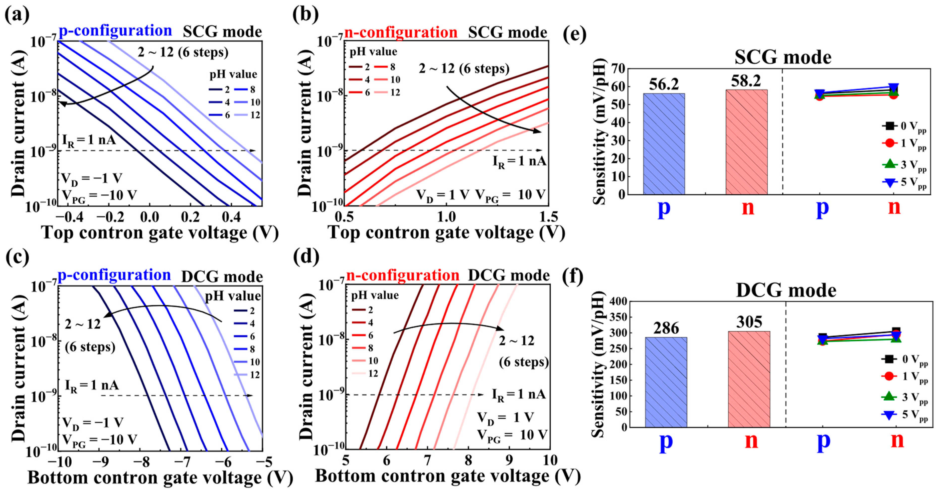
3.4.2. pH Sensing Performance of the R-ISFET Sensor

The pH sensing performance was evaluated in the SCG and DCG modes. Sensitivity was extracted from the threshold voltage shift (ΔVTH) at a reference drain current (IR) of 1 nA. The transfer characteristics for p-type and n-type configurations, recorded in the SCG mode with only the top gate active, are shown in Figure 6a,b, respectively. In the DCG mode, surface potential is sensed via the top gate while current is modulated through the bottom gate. The transfer curves are shown in Figure 6c (p-type) and Figure 6d (n-type). The sensitivities are presented in Figure 6e (SCG) and 6f (DCG). In the SCG mode, the p-type and n-type configurations exhibited sensitivities of 56.2 and 58.2 mV/pH, respectively—which approached the theoretical Nernst limit. In contrast, the DCG mode achieved significantly enhanced sensitivities of 286 and 305 mV/pH for p-type and n-type configurations, respectively, corresponding to a more than fivefold increase. These results match the theoretical amplification factor of ~6, calculated based on the CTox/CBox ratio. The superior sensitivity in the n-type configuration is attributed to the favorable electrochemical response and high carrier mobility of the SnO2 thin film, which is well-suited for n-type operation [50,51]. The capacitive coupling in the DCG architecture effectively amplifies the electrical response to surface potential variations, enabling sensitivities that surpass the Nernst limit and validating the sensor’s high-performance capability.
To evaluate noise immunity, sinusoidal signals of 0, 1, 3, and 5 Vpp were applied via reference electrode in both modes. The n-type DCG configuration maintained highest sensitivity with minimal degradation across noise levels, matching the expected amplification from CTox/CBox ratio, as shown in Figure 6e,f. The p-type configuration showed excellent noise immunity, with minor sensitivity variations across noise conditions.
These findings confirm that the DCG architecture enhances sensitivity through capacitive amplification while ensuring signal stability in noisy environments. The p-type configuration showed superior durability and stability, highlighting its potential for practical sensing applications.
Figure 6. Transfer characteristic curves of the R-ISFET measured in pH buffer solutions of 2, 4, 6, 8, 10, and 12 for (a) p-type and (b) n-type configurations under SCG mode, and for (c) p-type and (d) n-type configurations under DCG mode. The corresponding pH sensitivities and their variations under externally applied sinusoidal noise amplitudes of 0, 1, 3, and 5 Vpp are shown in (e) for the SCG mode and (f) for the DCG mode.
Chemosensors 13 00281 g006

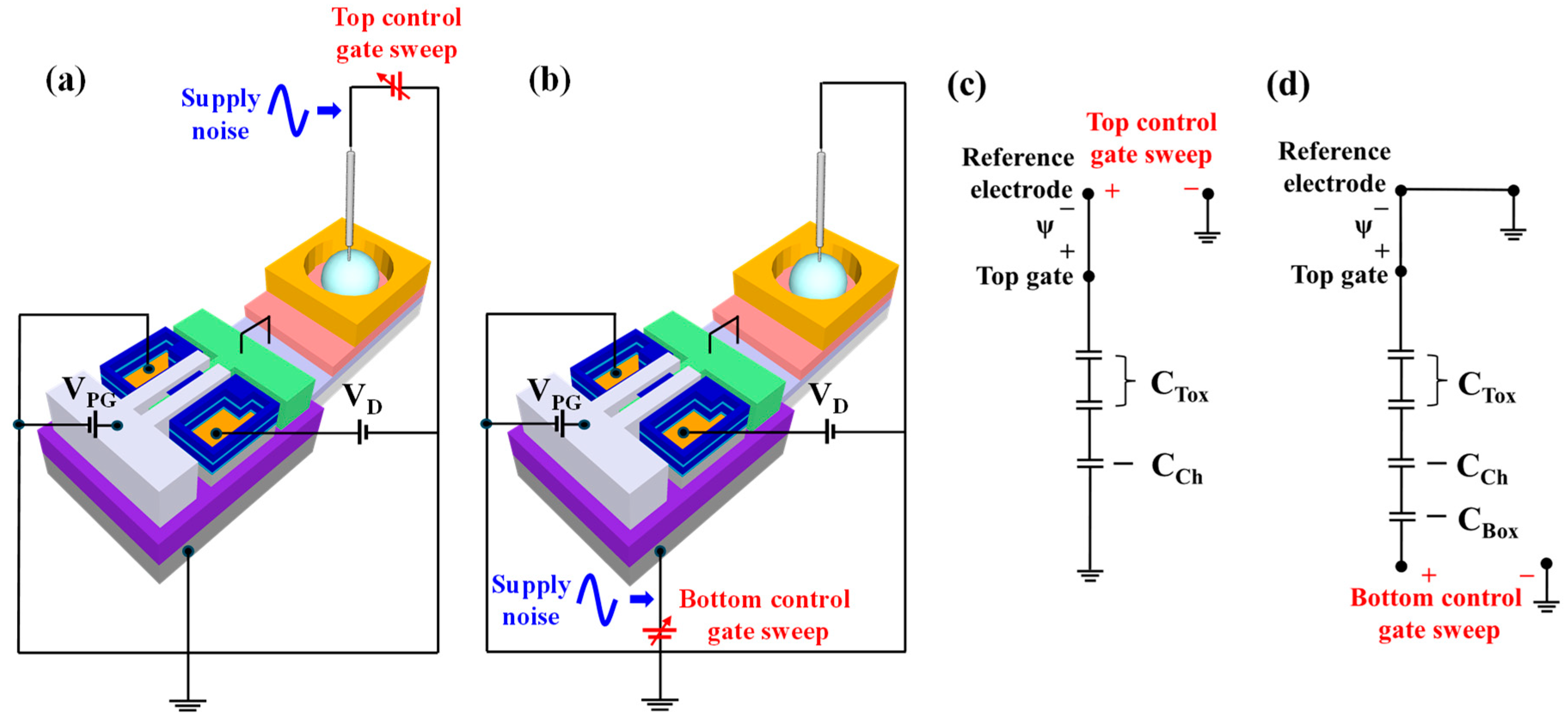
3.5. Non-Ideal Effects of the R-ISFET Sensor

To assess the practical applicability of the proposed R-ISFET sensor beyond its sensitivity, the electrical reliability and stability were evaluated under repeated use and prolonged operation. Hysteresis and drift—representative non-ideal effects commonly observed in ISFET-based sensors—served as critical indicators for assessing measurement repeatability, accuracy, and resistance to environmental variations. External electrical noise was applied to facilitate rigorous evaluation of these characteristics. The non-ideal effects were quantitatively analyzed under both SCG and DCG operation modes. Hysteresis characteristics are presented in Figure 7, while drift behavior is summarized in Figure 8.

3.5.1. Hysteresis Effect
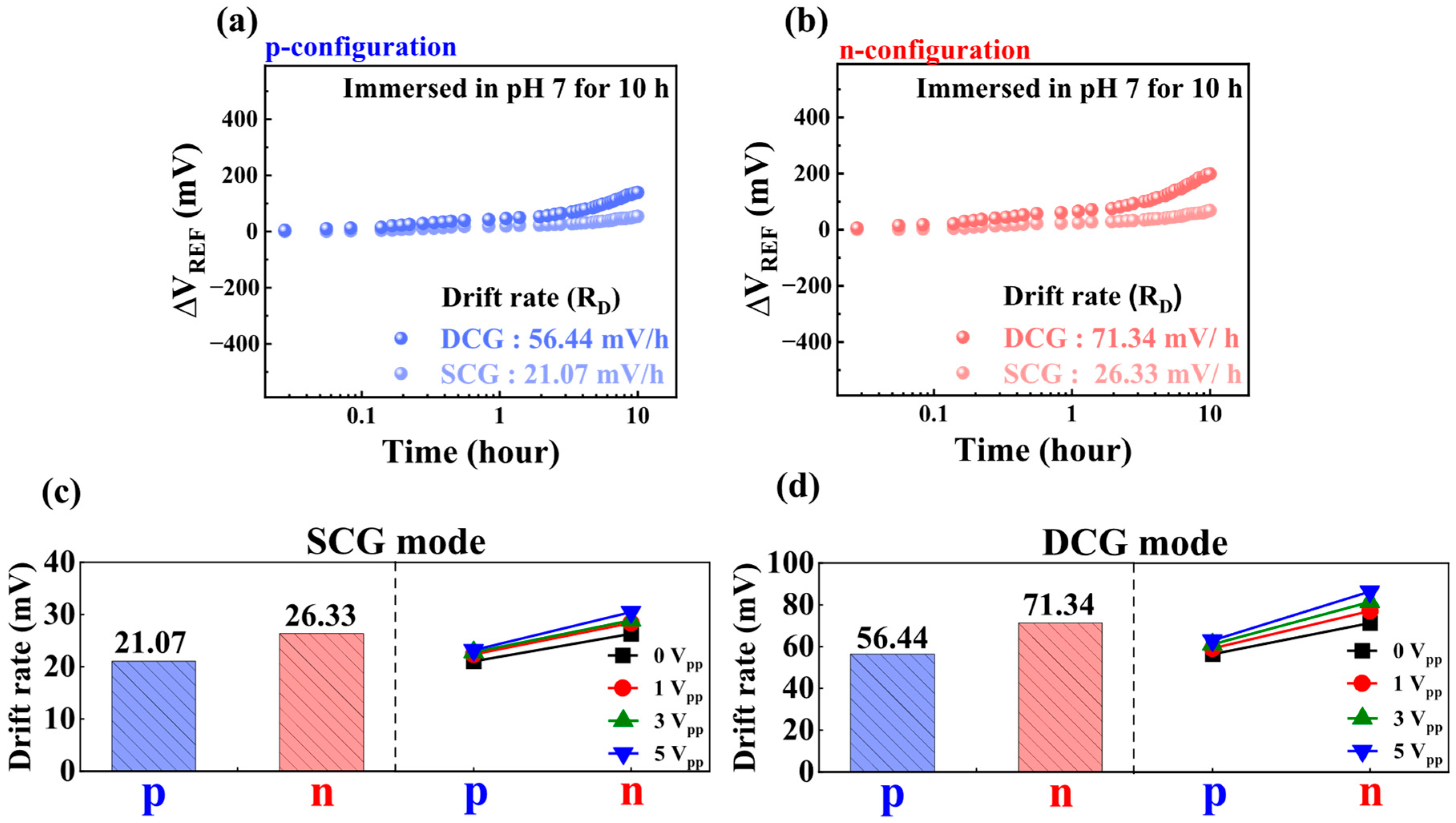
Hysteresis, the electrical memory effect during repeated pH measurements, was evaluated using a pH cycling sequence of 7 → 4 → 7 → 10 → 7. Measurements were taken after 2 min equilibrium periods. The hysteresis voltage (VH) was defined as the threshold voltage (VTH) difference between initial and final measurements at pH 7. The corresponding VTH shift based on the transfer curves is presented in Figure S4. This phenomenon is typically attributed to rapid proton exchange with surface hydroxyl (–OH) groups and slower ion diffusion into the bulk dielectric region [52,53,54]. VH was measured under SCG and DCG modes. For p-type configuration, hysteresis values were 9.8 and 26.1 mV, respectively, as shown in Figure 7a. For the n-type configuration, VH values were 11.4 mV (SCG) and 31.1 mV (DCG), as shown in Figure 7b. To evaluate noise immunity, sinusoidal noise amplitudes of 0, 1, 3, and 5 Vpp were applied via the reference electrode, with the hysteresis variations shown in Figure 7c,d. The p-type configuration maintained stable VH values across noise levels, while the n-type showed increased hysteresis with higher noise amplitudes.
Figure 7. Hysteresis characteristics of the R-ISFET sensor evaluated during pH cycling through values of 4, 7, and 10 under both SCG and DCG operation modes. Transfer characteristics and extracted VH are shown for (a) p-type and (b) n-type configurations. The corresponding VH values and their variations under external noise amplitudes of 0, 1, 3, and 5 Vpp are illustrated for (c) SCG mode and (d) DCG mode.
Chemosensors 13 00281 g007

3.5.2. Drift Effect

Drift, defined as the gradual VTH shift over time under constant conditions, was monitored by immersing the sensor in pH 7 buffer for 10 h. Drift typically results from ion diffusion through a hydration layer on the sensing membrane or from ion trapping at defect states within the dielectric interface [55,56]. In the extended gate structure, although the sensing membrane and transistor channel are electrically decoupled, drift still arises from slow ion adsorption and charge trapping within the sensing layer. These processes gradually modify the effective gate potential transmitted to the FET, resulting in shifts in device characteristics over time. For the p-type configuration, the VTH shift was 21.07 mV in SCG mode and 56.44 mV in DCG mode, as shown in Figure 8a. In the n-type configuration, the corresponding drift values were 26.3 mV and 71.34 mV, respectively, as shown in Figure 8b. The drift rate (RD) was analyzed under external noise of 0, 1, 3, and 5 Vpp, with the n-type showing higher sensitivity to noise than the p-type, as illustrated in Figure 8c,d.
Figure 8. Drift behavior of the R-ISFET sensor monitored over a 10 h immersion in a pH 7 buffer solution under SCG and DCG modes. Threshold voltage shifts over time are presented for (a) p-type and (b) n-type configurations. The corresponding drift magnitudes and their variations under external noise amplitudes of 0, 1, 3, and 5 Vpp are displayed for (c) SCG mode and (d) DCG mode.
Chemosensors 13 00281 g008
In summary, the p-type configuration showed stable performance in both hysteresis and drift tests, maintaining good noise immunity under external perturbations. Although the DCG mode exhibited larger hysteresis and drift than the SCG mode—due to voltage response amplification from capacitive coupling between dual gates—these increased values were modest compared to the sensitivity improvement. These results confirm that the sensor maintains sufficient electrical stability even in the DCG architecture, supporting its suitability for high-performance, noise-resilient sensing applications. In future work, the introduction of nanostructured sensing layers is expected to further mitigate non-ideal effects in the DCG mode while maintaining high sensitivity and enhancing the overall reliability of the sensor [57,58].

4. Conclusions

In this study, we demonstrated a novel bidirectional chemical sensing platform based on a R-ISFET architecture integrating Ni-silicide Schottky S/D contacts, dual-gate electrostatic control, and an EG configuration. This approach addresses conventional ISFET limitations using carrier polarity tunability and signal transduction enhancement within a single device. The Ni-silicide contacts minimized contact resistance and facilitated robust ambipolar conduction. Notably, the dual-gate configuration—comprising a PG and CG—enabled dynamic reconfiguration between the n-type and p-type modes without chemical doping. The PG modulated carrier injection at S/D junctions, whereas the CG governed channel potential, allowing leakage suppression and symmetric transfer characteristics for ambipolar behavior. The DCG mode induced strong capacitive coupling between the top and bottom gate dielectrics, resulting in enhanced pH sensitivity, which was fivefold of that achieved in the SCG mode. This improvement aligns with theoretical predictions (based on the dielectric capacitance ratio), enabling the sensor to surpass the Nernst limit without external amplification. Electrical characterization revealed distinct advantages: the n-type configuration showed higher field-effect mobility and sharper subthreshold swing, whereas the p-type configuration provided better electrical reliability with reduced hysteresis, drift, and stronger immunity against electrical noise. These characteristics validate the adaptive-sensing strategies that balance sensitivity and stability based on operational demands. The device achieved near-Nernst limited chemical sensitivity in the SCG mode and a high sensitivity of up to 305 mV/pH in the DCG mode. Despite enhanced sensitivity, the non-ideal effects remained within acceptable bounds, ensuring reliable long-term performance. The complementary behavior enables balanced sensitivity and stability trade-offs through dynamic mode switching. The adaptability, reconfigurable nature, and complementary electrical behavior further underscore the potential of the R-ISFET sensor as a flexible and robust next-generation platform for real-time biochemical sensing, PoC diagnostics, environmental monitoring, and lab-on-chip applications requiring high sensitivity and reliability.

Supplementary Materials

The following supporting information can be downloaded at: https://www.mdpi.com/article/10.3390/chemosensors13080281/s1, Figure S1: Fabrication details of the fabricated R-ISFET transducer; Figure S2: (a) Temperature profiles for the MWA process at 250–1000 W; Figure S3: (a) Sheet resistance of the NiSix samples obtained via MWA at powers of 250–1000 W for 2 min, (b) current–voltage (I-V) curves of the NiSix SB-diodes; Figure S4: Transfer characteristics for hysteresis evaluation of the R-ISFET sensor under SCG mode: (a) n-type configuration, (b) p-type configuration; DCG mode: (c) n-type configuration, (d) p-type configuration.

Author Contributions

Conceptualization, S.-J.L. and S.-H.L.; formal analysis, S.-J.L. and S.-H.L.; methodology S.-J.L. and S.-H.L.; investigation S.-J.L. and S.-H.L.; data curation, S.-J.L., S.-H.L. and S.-H.C.; visualization S.-J.L., S.-H.L. and S.-H.C.; writing—original draft preparation, S.-J.L. and S.-H.L.; writing—review and editing, W.-J.C.; supervision, W.-J.C.; All authors have read and agreed to the published version of the manuscript.

Funding

This work was supported by the Korea Institute for Advancement of Technology (KIAT) grant funded by the Korean government (MOTIE) (P0020967, The Competency Development Program for Industry Specialists), and by the Electronics and Telecommunications Research Institute (ETRI) grant funded by the Korean government (25ZC1300, Development of Future Display Integrated Devices and Process Technology).

Institutional Review Board Statement

Not applicable.

Informed Consent Statement

Not applicable.

Data Availability Statement

Data are contained within the article.

Acknowledgments

This research has been conducted with the help of the Research Grant of Kwangwoon University in 2025.

Conflicts of Interest

The authors declare no conflicts of interest.

References

  1. He, Y.; Wu, Y.; Mishra, A.; Acha, V.; Andrews, T.; Hornsby, P.J. Biosensor technology in aging research and age-related diseases. Ageing Res. Rev. 2012, 11, 1–9. [Google Scholar] [CrossRef]
  2. Pejcic, B.; De Marco, R.; Parkinson, G. The role of biosensors in the detection of emerging infectious diseases. Analyst 2006, 131, 1079–1090. [Google Scholar] [CrossRef]
  3. Kim, D.; Min, J.; Ko, S.H. Recent Developments and Future Directions of Wearable Skin Biosignal Sensors. Adv. Sens. Res. 2024, 3, 2300118. [Google Scholar] [CrossRef]
  4. Wadhera, T.; Kakkar, D.; Wadhwa, G.; Raj, B. Recent Advances and Progress in Development of the Field Effect Transistor Biosensor: A Review. J. Electron. Mater. 2019, 48, 7635–7646. [Google Scholar] [CrossRef]
  5. Singh, D.; Patil, G.C. Performance Analysis of Feedback Field-Effect Transistor-Based Biosensor. IEEE Sens. J. 2020, 20, 13269–13276. [Google Scholar] [CrossRef]
  6. Holgado, M.; Maigler, M.; Santamaría, B.; Hernandez, A.; Lavín, A.; Laguna, M.; Sanza, F.; Granados, D.; Casquel, R.; Portilla, J.; et al. Towards reliable optical label-free point-of-care (PoC) biosensing devices. Sens. Actuators B Chem. 2016, 236, 765–772. [Google Scholar] [CrossRef]
  7. Narayan, R. (Ed.) Medical Biosensors for Point of Care (POC) Applications; Woodhead Publishing: Cambridge, UK, 2016. [Google Scholar]
  8. Cheon, J.; Qin, J.; Lee, L.P.; Lee, H. Advances in Biosensor Technologies for Infection Diagnostics. Accounts Chem. Res. 2022, 55, 121–122. [Google Scholar] [CrossRef]
  9. Han, Y.D.; Chun, H.J.; Yoon, H.C. Low-cost Point-of-Care Biosensors Using Common Electronic Components as Transducers. BioChip J. 2020, 14, 32–47. [Google Scholar] [CrossRef]
  10. Shi, X.; Pu, H.; Shi, L.L.; He, T.-C.; Chen, J. Advancing transistor-based point-of-care (POC) biosensors: Additive manufacturing technologies and device integration strategies for real-life sensing. Nanoscale 2025, 17, 9804–9833. [Google Scholar] [CrossRef]
  11. Amen, M.T.; Pham, T.T.T.; Cheah, E.; Tran, D.P.; Thierry, B. Metal-Oxide FET Biosensor for Point-of-Care Testing: Overview and Perspective. Molecules 2022, 27, 7952. [Google Scholar] [CrossRef]
  12. Al-Younis, Z.K.; Almajidi, Y.Q.; Mansouri, S.; Ahmad, I.; Turdialiyev, U.; Alsaab, H.O.; Ramadan, M.F.; Joshi, S.K.; Alawadi, A.H.; Alsaalamy, A. Label-Free Field Effect Transistors (FETs) for Fabrication of Point-of-Care (POC) Biomedical Detection Probes. Crit. Rev. Anal. Chem. 2024, 1–22. [Google Scholar] [CrossRef]
  13. Gao, A.; Lu, N.; Wang, Y.; Li, T. Robust ultrasensitive tunneling-FET biosensor for point-of-care diagnostics. Sci. Rep. 2016, 6, 22554. [Google Scholar] [CrossRef]
  14. Li, J.; Wijaya, L.N.A.; Jang, D.W.; Hu, Y.; You, J.; Cai, Y.; Gao, Z.; Mi, Y.; Luo, Z. 2D Materials-Based Field-Effect Transistor Biosensors for Healthcare. Small 2025, 21, e2408961. [Google Scholar] [CrossRef]
  15. Cao, S.; Sun, P.; Xiao, G.; Tang, Q.; Sun, X.; Zhao, H.; Zhao, S.; Lu, H.; Yue, Z. ISFET-based sensors for (bio)chemical applications: A review. Electrochem. Sci. Adv. 2023, 3, e2100207. [Google Scholar] [CrossRef]
  16. Rani, D.; Singh, Y.; Salker, M.; Vu, X.T.; Ingebrandt, S.; Pachauri, V. Point-of-care-ready nanoscale ISFET arrays for sub-picomolar detection of cytokines in cell cultures. Anal. Bioanal. Chem. 2020, 412, 6777–6788. [Google Scholar] [CrossRef] [PubMed]
  17. Pijanowska, D.G.; Torbicz, W. pH-ISFET based urea biosensor. Sens. Actuators B Chem. 1997, 44, 370–376. [Google Scholar] [CrossRef]
  18. Chou, J.C.; Wang, Y.F. Preparation and study on the drift and hysteresis properties of the tin oxide gate ISFET by the sol–gel method. Sens. Actuators B Chem. 2002, 86, 58–62. [Google Scholar] [CrossRef]
  19. Bergveld, P. Development of an Ion-Sensitive Solid-State Device for Neurophysiological Measurements. IEEE Trans. Biomed. Eng. 1970, BME–17, 70–71. [Google Scholar] [CrossRef] [PubMed]
  20. Bergveld, P. Thirty years of ISFETOLOGY: What happened in the past 30 years and what may happen in the next 30 years. Sens. Actuators B Chem. 2003, 88, 1–20. [Google Scholar] [CrossRef]
  21. Jakobson, C.G.; Nemirovsky, Y. 1/f noise in ion sensitive field effect transistors from subthreshold to saturation. IEEE Trans. Electron Devices 1999, 46, 259–261. [Google Scholar] [CrossRef]
  22. Panahi, A.; Sadighbayan, D.; Forouhi, S.; Ghafar-Zadeh, E. Recent Advances of Field-Effect Transistor Technology for Infectious Diseases. Biosensors 2021, 11, 103. [Google Scholar] [CrossRef]
  23. Kim, Y.-U.; Cho, W.-J. High-Performance Bidirectional Chemical Sensor Platform Using Double-Gate Ion-Sensitive Field-Effect Transistor with Microwave-Assisted Ni-Silicide Schottky-Barrier Source/Drain. Chemosensors 2022, 10, 122. [Google Scholar] [CrossRef]
  24. Mikolajick, T.; Heinzig, A.; Trommer, J.; Baldauf, T.; Weber, W. The RFET—A reconfigurable nanowire transistor and its application to novel electronic circuits and systems. Semicond. Sci. Technol. 2017, 32, 043001. [Google Scholar] [CrossRef]
  25. Zheng, S.; Zhou, J.; Wang, C.; Li, K.; Fang, C.; Li, X.; Liang, J.; Liu, Y.; Hao, Y.; Han, G. A Ferroelectric Reconfigurable Memory with Excitatory and Inhibitory Synaptic Responses. In Proceedings of the 2024 IEEE International Conference on IC Design and Technology (ICICDT), Singapore, 25–27 September 2024; pp. 1–4. [Google Scholar] [CrossRef]
  26. Jang, H.-J.; Cho, W.-J. Performance Enhancement of Capacitive-Coupling Dual-gate Ion-Sensitive Field-Effect Transistor in Ultra-Thin-Body. Sci. Rep. 2014, 4, 5284. [Google Scholar] [CrossRef]
  27. Kang, J.W.; Cho, W.J. Achieving enhanced pH sensitivity using capacitive coupling in extended gate FET sensors with various high-K sensing films. Solid-State Electron. 2019, 152, 29–32. [Google Scholar] [CrossRef]
  28. Cho, S.-K.; Cho, W.-J. Ultra-high sensitivity pH-sensors using silicon nanowire channel dual-gate field-effect transistors fabricated by electrospun polyvinylpyrrolidone nanofibers pattern template transfer. Sens. Actuators B Chem. 2021, 326, 128835. [Google Scholar] [CrossRef]
  29. Bhatt, D.; Panda, S. Dual-Gate Ion-Sensitive Field-Effect Transistors: A Review. Electrochem. Sci. Adv. 2021, 1, 10. [Google Scholar] [CrossRef]
  30. Biswas, A.; Rajan, C.; Samajdar, D.P. A Novel RFET Sensor for Label-Free Biomolecule Detection. Silicon 2022, 14, 9533–9541. [Google Scholar] [CrossRef]
  31. Reyes, P.I.; Ku, C.-J.; Duan, Z.; Lu, Y.; Solanki, A.; Lee, K.-B. ZnO Thin Film Transistor Immunosensor with High Sensitivity and Selectivity. Appl. Phys. Lett. 2011, 98, 173702. [Google Scholar] [CrossRef]
  32. Lee, J.; Dak, P.; Lee, Y.; Park, H.; Choi, W.; Alam, M.A.; Kim, S. Two-Dimensional Layered MoS2 Biosensors Enable Highly Sensitive Detection of Biomolecules. Sci. Rep. 2014, 4, 7352. [Google Scholar] [CrossRef] [PubMed]
  33. Ma, S.; Li, X.; Lee, Y.-K.; Zhang, A. Direct Label-Free Protein Detection in High Ionic Strength Solution and Human Plasma Using Dual-Gate Nanoribbon-Based Ion-Sensitive Field-Effect Transistor Biosensor. Biosens. Bioelectron. 2018, 117, 276–282. [Google Scholar] [CrossRef]
  34. Pullano, S.A.; Critello, C.D.; Mahbub, I.; Tasneem, N.T.; Shamsir, S.; Islam, S.K.; Greco, M.; Fiorillo, A.S. EGFET-Based Sensors for Bioanalytical Applications: A Review. Sensors 2018, 18, 4042. [Google Scholar] [CrossRef] [PubMed]
  35. van der Spiegel, J.; Lauks, I.; Chan, P.; Babic, D. The extended gate chemically sensitive field effect transistor as multi-species microprobe. Sens. Actuators 1983, 4, 291–298. [Google Scholar] [CrossRef]
  36. Chen, J.-C.; Chou, J.-C.; Sun, T.-P.; Hsiung, S.-K. Portable urea biosensor based on the extended-gate field effect transistor. Sens. Actuators B Chem. 2003, 91, 180–186. [Google Scholar] [CrossRef]
  37. Knoll, L.; Zhao, Q.T.; Habicht, S.; Urban, C.; Ghyselen, B.; Mantl, S. Ultrathin Ni Silicides With Low Contact Resistance on Strained and Unstrained Silicon. IEEE Electron Device Lett. 2010, 31, 350–352. [Google Scholar] [CrossRef]
  38. Kim, G.B.; Yoo, D.-J.; Baik, H.K.; Myoung, J.-M.; Lee, S.M.; Oh, S.H.; Park, C.G. Improved thermal stability of Ni silicide on Si (100) through reactive deposition of Ni. J. Vac. Sci. Technol. B Microelectron. Nanometer Struct. Process. Meas. Phenom. 2003, 21, 319–322. [Google Scholar] [CrossRef]
  39. Min, J.-G.; Lee, D.-H.; Kim, Y.-U.; Cho, W.-J. Implementation of Ambipolar Polysilicon Thin-Film Transistors with Nickel Silicide Schottky Junctions by Low-Thermal-Budget Microwave Annealing. Nanomaterials 2022, 12, 628. [Google Scholar] [CrossRef]
  40. Seger, J.; Hellström, P.-E.; Lu, J.; Malm, B.G.; von Haartman, M.; Östling, M.; Zhang, S.-L. Lateral encroachment of Ni-silicides in the source/drain regions on ultrathin silicon-on-insulator. Appl. Phys. Lett. 2005, 86, 253507. [Google Scholar] [CrossRef]
  41. Bhaskaran, M.; Sriram, S.; Mitchell, D.; Short, K.; Holland, A.; Mitchell, A. Microstructural investigation of nickel silicide thin films and the silicide–silicon interface using transmission electron microscopy. Micron 2009, 40, 11–14. [Google Scholar] [CrossRef]
  42. Chiu, W.-L.; Chiu, C.-H.; Chen, J.-Y.; Huang, C.-W.; Huang, Y.-T.; Lu, K.-C.; Hsin, C.-L.; Yeh, P.-H.; Wu, W.-W. Single-crystalline δ-Ni2Si nanowires with excellent physical properties. Nanoscale Res. Lett. 2013, 8, 290. [Google Scholar] [CrossRef]
  43. Navarro, C.; Barraud, S.; Martinie, S.; Lacord, J.; Jaud, M.-A.; Vinet, M. Reconfigurable field effect transistor for advanced CMOS: Advantages and limitations. Solid-state Electron. 2017, 128, 155–162. [Google Scholar] [CrossRef]
  44. Nishioka, Y.; Shinriki, H.; Mukai, K. Influence of SiO2 at the Ta2O5/Si interface on dielectric characteristics of Ta2O5 capacitors. J. Appl. Phys. 1987, 61, 2335–2338. [Google Scholar] [CrossRef]
  45. Krauss, T.; Wessely, F.; Schwalke, U. An electrostatically doped planar device concept. In Proceedings of the 9th IEEE International Conference on Design & Technology of Integrated Systems in Nanoscale Era (DTIS), Santorini, Greece, 6–8 May 2014; pp. 1–4. [Google Scholar] [CrossRef]
  46. Kim, J.B.; Fuentes-Hernandez, C.; Kim, S.-J.; Potscavage, W., Jr.; Choi, S.; Kippelen, B. Ambipolar thin-film transistors with a co-planar channel geometry. Org. Electron. 2010, 11, 1351–1356. [Google Scholar] [CrossRef]
  47. Nomura, K.; Kamiya, T.; Hosono, H. Ambipolar oxide thin-film transistor. Adv. Mater. 2011, 23, 3431–3434. [Google Scholar] [CrossRef]
  48. Go, J.; Nair, P.R.; Alam, M.A. Theory of signal and noise in double-gated nanoscale electronic pH sensors. J. Appl. Phys. 2012, 112, 34516. [Google Scholar] [CrossRef]
  49. Wu, T.; Alharbi, A.; You, K.-D.; Kisslinger, K.; Stach, E.A.; Shahrjerdi, D. Experimental study of the detection limit in dual-gate biosensors using ultrathin silicon transistors. ACS Nano 2017, 11, 7241–7249. [Google Scholar] [CrossRef]
  50. Um, J.; Kim, S.E. Homo-Junction pn Diode Using p-Type SnO and n-Type SnO2 Thin Films. ECS Solid State Lett. 2014, 3, P94–P98. [Google Scholar] [CrossRef]
  51. Achour, R.; Said, B.; Boubaker, B. Preparation of n-type semiconductor SnO2 thin films. J. Semicond. 2013, 34, 083002. [Google Scholar] [CrossRef]
  52. Kurzweil, P. Metal oxides and ion-exchanging surfaces as pH sensors in liquids: State-of-the-art and outlook. Sensors 2009, 9, 4955–4985. [Google Scholar] [CrossRef]
  53. Varghese, O.K.; Grimes, C.A. Metal Oxide Nanoarchitectures for Environmental Sensing. J. Nanosci. Nanotechnol. 2003, 3, 277–293. [Google Scholar] [CrossRef] [PubMed]
  54. Peighambardoust, S.J.; Rowshanzamir, S.; Amjadi, M. Review of the proton exchange membranes for fuel cell applications. Int. J. Hydrog. Energy 2010, 35, 9349–9384. [Google Scholar] [CrossRef]
  55. Kim, S.; Kwon, D.W.; Kim, S.; Lee, R.; Kim, T.-H.; Mo, H.-S.; Kim, D.H.; Park, B.-G. Analysis of current drift on p-channel pH-Sensitive SiNW ISFET by capacitance measurement. Curr. Appl. Phys. 2018, 18, S68–S74. [Google Scholar] [CrossRef]
  56. Chen, D.Y.; Chan, P.K. An Intelligent ISFET Sensory System with Temperature and Drift Compensation for Long-Term Monitoring. IEEE Sens. J. 2008, 8, 1948–1959. [Google Scholar] [CrossRef]
  57. Zeng, H.; Takahashi, T.; Kanai, M.; Zhang, G.; He, Y.; Nagashima, K.; Yanagida, T. Long-Term Stability of Oxide Nanowire Sensors via Heavily Doped Oxide Contact. ACS Sens. 2017, 2, 1854–1859. [Google Scholar] [CrossRef]
  58. Jakob, M.H.; Dong, B.; Gutsch, S.; Chatelle, C.; Krishnaraja, A.; Weber, W.; Zacharias, M. Label-Free SnO2 Nanowire FET Biosensor for Protein Detection. Nanotechnology 2017, 28, 245503. [Google Scholar] [CrossRef]
Figure 1. (a) Three-dimensional schematic of the R-ISFET architecture. (b) Optical microscopy image of the fabricated R-ISFET transducer, showing the defined channel region and electrode configuration. (c) Schematic of the SnO2-based EG sensing structure, featuring a PDMS reservoir positioned above the sensing membrane to contain the pH buffer solution, with the Ag/AgCl reference electrode immersed in the solution. (d) Photograph of the fully fabricated EG sensing unit.
Chemosensors 13 00281 g001
Figure 2. (a) Comparison of the sheet resistance of p-type silicon before and after Ni silicidation using MWA. (b) XRD patterns of Ni films deposited on p-type Si, comparing the as-deposited state with the state after MWA treatment. (c) I–V characteristics of Ni/p-Si Schottky diodes, demonstrating enhanced rectifying behavior following MWA-induced silicidation.
Chemosensors 13 00281 g002
Figure 3. (a) Transfer characteristics of the R-ISFET under top CG sweep, with fixed PG voltages of −10 V and +10 V corresponding to p-type and n-type configurations, respectively. (b) Transfer characteristics under bottom CG sweep, using the same PG voltage conditions as in (a). (c) Energy band diagrams corresponding to (a), illustrating carrier injection and tunneling behavior modulated by the top gate bias at representative bias states. (d) Energy band diagrams corresponding to (b), showing modulation of the channel potential via the bottom gate and the resulting Schottky barrier profiles at the source/drain junctions.
Chemosensors 13 00281 g003
Figure 4. Electrical characteristics of the R-ISFET under both p-type and n-type configurations. (a) Transfer characteristic curves obtained by sweeping the top CG while varying the VPG from ±2 V to ±10 V for p-type and n-type configurations, respectively. (b) Output characteristic curves measured under VPG = ±10 V for both configurations, with the top CG swept from |VGVTH| = 0 to 5 V in 11 steps. (c) Transfer characteristic curves acquired by sweeping the bottom CG under the same VPG conditions as in (a). (d) Output characteristic curves corresponding to (c), measured over the same |VGVTH| range using the bottom CG.
Chemosensors 13 00281 g004
Table 1. Extracted electrical parameters of the R-ISFET under top and bottom CG operation, based on the transfer characteristics.
Operation ModeConfigurationVTH (V)Ion/off (A/A)μFE (c m 2 /V∙s)SS (mV/dec)
Top CG operationn1.6 2.09   × 105464347
p−1.1 6.07   × 104371328
Bottom CG operationn2.1 1.92   × 106262575
p−1.5 1.10   × 106204600
Disclaimer/Publisher’s Note: The statements, opinions and data contained in all publications are solely those of the individual author(s) and contributor(s) and not of MDPI and/or the editor(s). MDPI and/or the editor(s) disclaim responsibility for any injury to people or property resulting from any ideas, methods, instructions or products referred to in the content.

