Article

Nanostructured Diamond Composites for Multifunctional Sensing Applications

1
Department of Physics, University of Puerto Rico, San Juan, PR 00936, USA
2
Department of Chemistry, Biochemistry, Physics, and Engineering, Indiana University of Pennsylvania, Indiana, PA 15705, USA
*
Authors to whom correspondence should be addressed.
Chemosensors 2022, 10(11), 488; https://doi.org/10.3390/chemosensors10110488
Submission received: 9 October 2022 / Revised: 30 October 2022 / Accepted: 15 November 2022 / Published: 17 November 2022

Abstract

:
We report studies of multifunctional, nanostructured diamond composites that were fabricated using chemical vapor deposition (CVD) techniques. Grain sizes from micrometer, to submicron, nano, and ultrananocrystalline diamond (UNCD) were controlled by varying CH4, hydrogen, and argon gas concentrations during the syntheses. Scanning electron microscopy (SEM) and Raman scattering spectroscopy were used to investigate the morphologies, composites, and crystallinities of the films. Four multifunctional sensor prototypes were designed, fabricated, and tested, based on the four diamond materials of different grain sizes. The responses of the four prototypes to either pollution gas or UV light illumination were systematically investigated at different operating temperatures. Experimental data indicated the obtained UNCD composite from the low-cost simple CVD fabrication technique appeared to have very good sensitivities when exposed to low concentrations of H2 or NH3 gas with a decent response and fast recovery time. Furthermore, highly induced photocurrents from both microdiamond- and UNCD-based prototypes to deep UV illumination were also demonstrated, with responsivities up to 2750 mA/W and 550 mA/W at 250 nm wavelength, respectively. Overall, the fabricated UNCD prototypes displayed a good balance in performance for multifunctional sensor applications in terms of responsivity, stability, and repeatability.

1. Introduction

Multifunctional nanocomposites that respond to multiple external stimuli enable novel electronic applications. There are not too many such materials available in nature. However, these properties can be created or enhanced by designing and developing nanostructured materials. Nanostructure-related properties have provided new insight into the materials world and opened up new applications. During the last few decades, various multifunctional nanostructures [1,2] have been intensively studied due to the global ecological challenge and outer space exploration. With the concerns of economic feasibility and application in often harsh environmental conditions, studies on sensing devices have been focused on high sensitivity, fast response rate, long-term stability, and miniature size.
Diamond is a promising candidate to answer these concerns, due to its wide bandgap, thermal and chemical stability, and robustness [3,4]. As a natural insulator with a 5.5 eV bandgap, diamond can be doped with group III or V elements to be transformed into semiconductors. The semiconductive diamond with a tunable bandgap has shown a wide range of UV radiation detection with a fast response [5]. Recent advances in high-quality diamond material growth have resulted in significant progress in developing diamond-based UV photodetectors. For example, using CVD techniques, Iwakaji et al. synthesized high-quality single crystalline diamond films, and then developed several UV photodetectors based on undoped and B-doped homoepitaxial diamond material [6]. Pace and De Sio fabricated two types of photoconductive UV detectors based on either single crystal or polycrystalline diamond films. The results showed that the sensitivity of the single crystal diamond-based detector is higher than that of the polycrystalline one [7]. Recently, C.R. Lin et al. focused on nanocrystalline diamond films for the fabrication of UV photodetectors [8]. The as-prepared detector has properties of high signal response and fast time response, but with slightly high input of UV light intensity up to 30 mW/cm2. K. Tang et al. also prepared and characterized several different diamond films with different grain sizes. They believed that the diamond film with a larger grain would be more suitable for a UV photodetector. The main challenge with this diamond structure has been the difficulty in synthesizing high-quality diamond [9]. Obtaining high purity, defect-free diamond films with minimal dislocations of the substrate has proven to be challenging [10,11,12]. Moreover, high temperature (>1000 °C) and ultrahigh vacuum (UHV) are required in the production of diamond material, which can cause serious stresses between the active layer and the substrate, besides increasing the cost of production significantly [13,14].
Recently, the development of innovative sensing devices has shown considerable progress, partially attributed to newly developed techniques employed in the growth of high-quality UNCD with extremely low cost [15]. These materials have been successfully employed to create various types of device architectures including sensing and microelectromechanical system (MEMS) devices [16,17]. In our previous papers, ultrananocrystalline diamond nanowire-based sensors were fabricated using the e-beam lithography technique at a relatively high cost [18,19,20,21,22]. However, there are scarce reports of diamond-based multifunctional sensors.
In this paper, we focus on the study of the synthesis of diamond thin films of different grain sizes and composites, as well as the evaluation of their direct applications to form high-performance sensing devices with extremely low-cost fabrication techniques. Four types of multifunctional nanostructured diamond composites with grain sizes varying from micrometer to submicron, nano, and UNCD were fabricated using chemical vapor deposition (CVD) techniques. Scanning electron microscopy (SEM) and Raman scattering spectroscopy were used to investigate the morphologies, composites, and crystallinities of these films. The electrical and sensing properties of four types of diamond thin films were studied in different thermal, pollution gas, and UV light radiation environments. Several unusual electric and electronic properties were observed. Furthermore, prototypes based on these four types of diamond thin films were designed, fabricated, and tested. The experimental data indicated these nanocomposite-based prototypes appeared to have a very good sensitivity when exposed to either a low concentration of pollution gas like NH3 or low intensity of UV light illumination. Quick response, fast recovery time, highly stable baseline, and excellent reproducibility have been achieved.

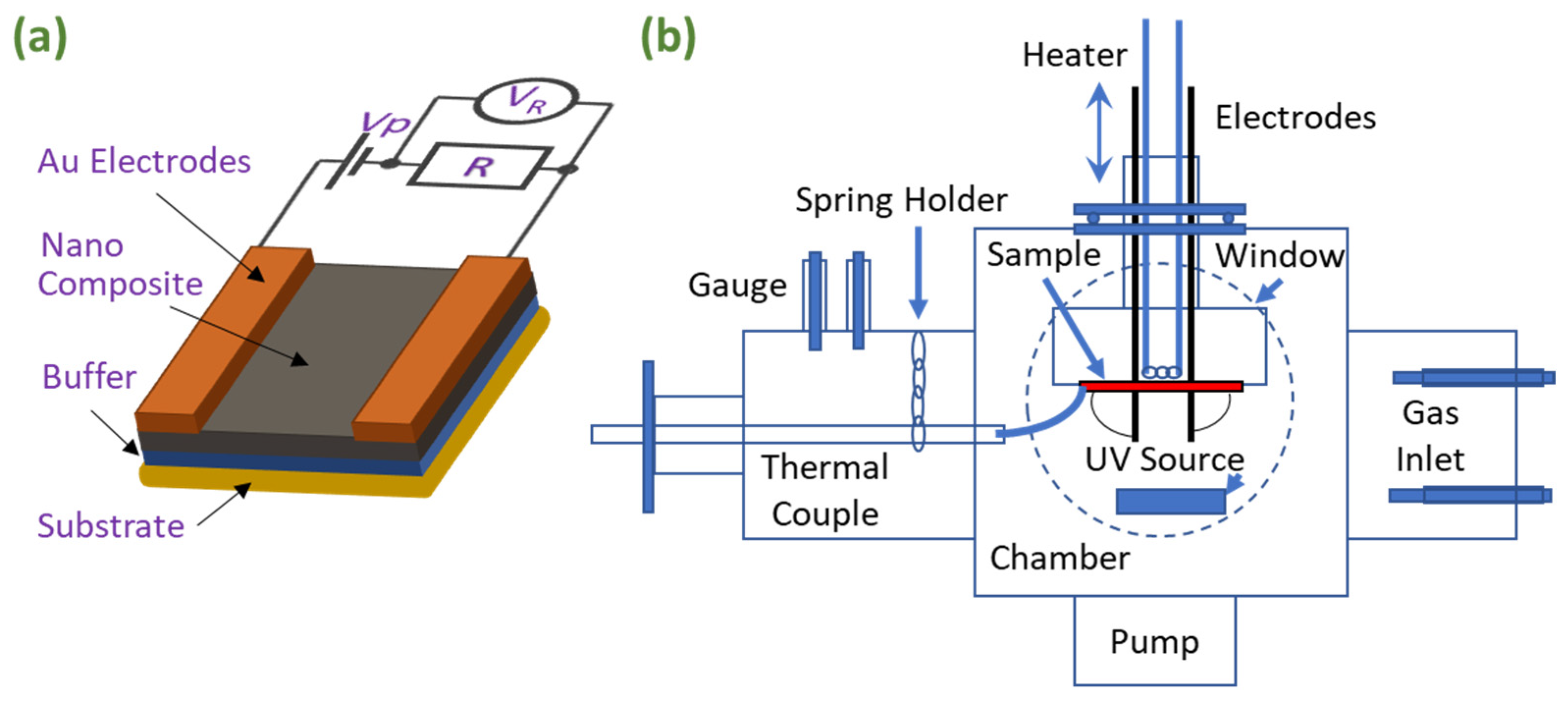
2. Materials and Methods

Both hot filament (HF)-assisted and microwave plasma (MP)-assisted chemical vapor deposition (CVD) were used to fabricate nanostructured diamond material with controllable grain sizes from micrometer, to submicron, nano, and UNCD. The obtained nanostructures highly relied on the CH4, hydrogen, and argon gas concentrations used during the syntheses. Detailed descriptions of the hot filament-assisted and microwave plasma-assisted chemical vapor deposition (CVD) can be found in our previous papers [23]. Briefly, a mixture of methane, hydrogen, and argon gases with methane concentrations from 0.2%, 1% to 2.5% and a total flow rate of 150 sccm was used in an HF-CVD to fabricate micrometer, submicron, and nanodiamond, respectively. In contrast, hydrogen gas was nearly removed in an MP-CVD to fabricate UNCD films.
The synthesis equipment contained a microwave generator of 2.45 GHz or 915 MHz frequency and up to 2 kW power. The chamber was maintained at around 100 Torr with a gas mixture of 95–99% Ar, 0–1% N2, and 1% CH4 where the N2 component was used for doping purposes in order to obtain a reasonable conductivity of nitrogen-doped UNCD (N-UNCD). Driven by the microwave plasmas, the collision between electrons and gases generated a high fraction of ionized species and therefore provided abundant chemically active ions for UNCD growth. The substrate temperature was maintained at around 600 °C. For UNCD growth, the structural formation of diamond was accelerated and simplified at a much higher renucleation rate. The N-doping and the n-type conduction have been confirmed by the EDS spectrum [14] as well as Hall and Seebeck coefficient measurements [24]. The formed n-type N-UNCD used in this investigation was synthesized with 1 vol.% nitrogen in the reactor. Approximately 70 nm-thick N-UNCD thin film was obtained for a typical growth time of one hour.
For simplification, N-UNCD, nano, submicron, and micrometer samples have been marked with S1–S4, respectively, in the following parts. The morphologies of these samples were investigated using scanning electron microscopy (SEM). Atomic force microscopy (AFM-Veeco) was employed to reveal the surface topography, such as grain size and surface roughness down to the nanometer scale. Raman scattering spectra of the samples were obtained at room temperature using a triple monochromator (ISA J-Y Model T64000) with an excitation wavelength of 514 nm (Ar+ ion laser). After basic characterizations, Au electrodes were deposited onto two ends of each sample. Then, electrical, electronic, and sensing properties were examined in a homemade characterization station where various components including thermocouple, heater, power supply, electrical connectors, pollution gas tanks, visible and UV lights, spectroscopic diagnostics, UV power meter, multichannel Pascal universal interface, as well as various Agilent and Hewlett meters were available. Each sensing sample was connected to a precise resistor R, a switcher, and a power supply Vp to form a prototype. Variations in its resistance due to the adsorption of external gas molecules in a gas sensing system or the induced photocurrent due to light illumination in a light sensing system were recorded.

3. Results and Discussion

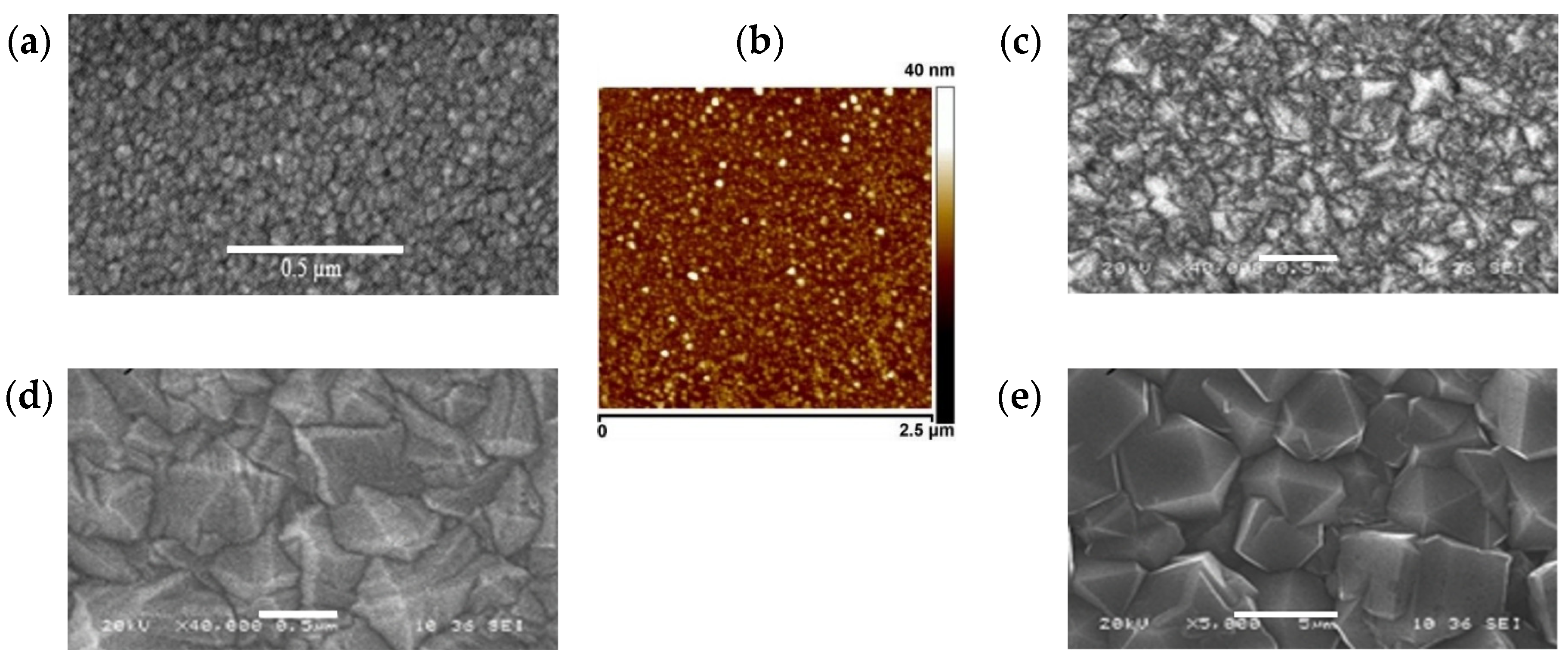
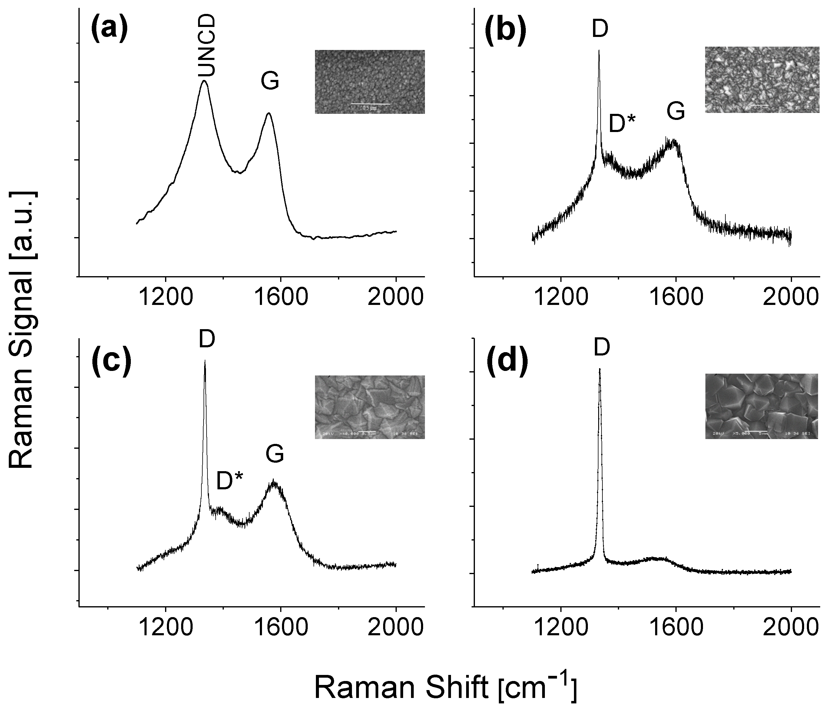
3.1. Material Characterizations

Figure 1 shows the typical SEM images of the N-UNCD, nano, submicron, and micrometer sizes of grains of the four samples S1–S4. Different morphologies of the samples are clearly visible. Figure 1a indicates that the N-UNCD film mainly consisted of extremely small diamond particles. AFM was used to observe its morphologies, as shown in Figure 1b, which reveals a very dense diamond nanoparticle layer with diamond nanoparticles of an average 3–5 nm diameter uniformly distributed on the surface. The root mean square (RMS) roughness of the seeded substrate is around 5 nm, which did not change with the increase in N-UNCD film thickness. This characteristic brings the most diminutive dimensions of miniature N-UNCD devices down to the limit of the top-down or bottom-up nanomanufacturing technology with the e-beam lithography (EBL)/reactive ion etch (RIE), as we did before [25]. However, N-UNCD film in the present work is characterized and used for sensing devices directly, which provides an extremely low-cost alternative.
Figure 1c–e show SEM images of three HFCVD fabricated diamond composites. An increase in the concentration of methane from 0.2, 1 to 2.5% leads to a decrease in diamond grain size from 5 µm, 0.5 µm to 0.1 µm. The quality of the crystalline structure of the synthesized composite highly relies on the synthesis conditions. A low concentration of methane in HFCVD normally yields very prism-type edge particles, suggesting a good 111 orientation of the crystalline structure, in good agreement with previous reports [26].
Raman analysis of the four samples S1–S4 was conducted at room temperature, using 514 nm excitation from an Ar+ laser at an irradiance of approximately 5 mW/cm2. The results obtained are presented in Figure 2. The observed Raman scattering spectra are predominantly from the sp2-bonded carbon, even though there is a significant amount of sp3-bonded carbon in the sample. One of the possible reasons is that the sp2 sites have a much larger cross section than the sp3 sites, as explained by the well-known resonant effect of Raman scattering. As shown in Figure 2a, the Raman spectra of ultrananocrystalline diamond are dominated by the D band (UNCD) peak at 1330 cm−1 and the broad G band peak centered at 1580 cm−1 due to the in-plane stretching modes of the sp2-bonded carbon at the grain boundaries of UNCD [27,28,29,30].
The sharp peak at 1333 cm−1 is clearly visible from the S2 sample (Figure 2b), and it is further enhanced in the S4 sample (Figure 2d). This peak labeled with D is associated with the characteristics of sp3 carbon networks. The diamond consists of highly uniformed C-C bonds in a tetrahedral crystal structure. All the bonds in the crystal are of the same orientation and strength. In the S2–S4 system, the board peak marked with G positioned at 1585 cm−1 is also ascribed to the sp2 carbon network known as the G band of graphite. When the diamond is dominating, we can only observe a single vibrational frequency. As seen when the synthesis condition changes as the concentration of methane increases, the G band from the obtained sample begins to emerge and rises. Another tiny peak centering at 1370 cm−1 marked with D* could also be observed in the S2 Raman spectrum, but its signal intensity decreased following a decrease in methane concentration to 0.2%. In general, the D* band is associated with impurity and defect. The integrated intensity ratio ID/IG for the D* and G bands can be used for characterizing the quantity in graphite materials, which has been reported previously [23,27,28].

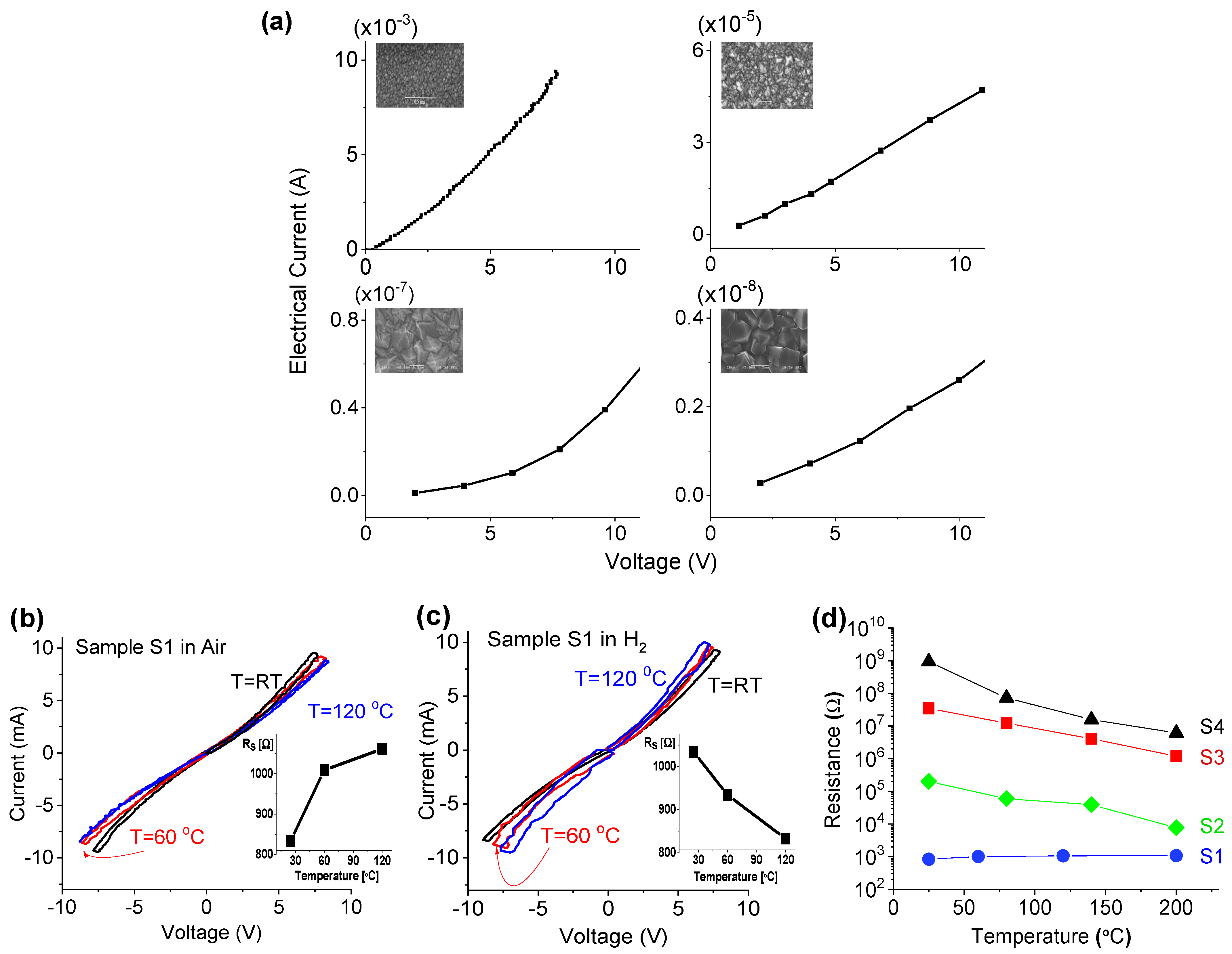
3.2. Electrical Properties

To characterize the electrical property of the sample, 80–100 nm-thick Au electrodes were deposited onto the two ends of the synthesized thin film, resulting in an active layer of a total exposure area of 2 × 1 mm2. The metal–semiconductor–metal (MSM) structure was chosen since it provided the advantages of high responsivity, high speed, and fabrication simplicity. The prototypic sensing device was constructed using a simple electrical circuit, as illustrated in Figure 3a. The electrical transport and sensing properties were characterized using a Keithley 6430 sub-femtoampere source meter connected to a micromanipulator probe station (Figure 3b) by recording I–V curves ranging from −15.0 V to 15.0 V with a 0.1 V step size. Each sample was simply mounted individually on the stage that was in direct contact with a heater element located underneath the stage for the temperature control of the sample.
The typical I–V characteristics of S1–S4 samples are shown in Figure 4a. The measurements were carried out in open-air ambient conditions at room temperature. The obtained curves of S1 and S2 appeared to be slightly more linear than S3 and S4, especially when the bias voltage was further increased. These phenomena can be directly ascribed to the different levels of impurities on the sample surface. At the interface between the metal and the semiconductor, a narrow depletion region is in general caused by a high concentration of dopant or treatment, i.e., it leads to small contact resistance and yields a good ohm contact.
The samples have very different conductance. The S1 sample has the highest conductance, the S2 sample has the second-highest conductivity, and the S4 sample has the lowest conductance. For regular diamond materials (sample S2, S3 or S4), the concentration of graphite intensively affects the electrical properties of nanodiamond composite films as well as their interfaces. When a large amount of graphite is introduced into the diamond film (S2), the concentration of the defect inside the composite would become high, resulting in an increase in the mobility of electrons and holes that lower the resistance of the composite. Following the decrease in concentration of the graphite inside the composites (S3 and S4), the diamond grains become dominant, resulting in an increase in resistance. Meanwhile, Schottky contact becomes governing on the interface. The evidence is nonlinear current–voltage (I–V) characteristics begin to emerge and rise.
Interestingly, the N-UNCD used in this investigation has a different conduction mechanism. As an insulator, high quality undoped UNCD has low electrical conduction naturally. However, the present N-UNCD synthesized with N2 additives has shown to behave like an n-type semiconductor. The nitrogen (N2) introduced in the conventional Ar-diluted CH4 and H2 gas mixture employed for the MPCVD process enlarged grain boundaries containing mainly sp2 bonded carbon (graphite-like) converted from the sp3 (diamond) phase. Although nitrogen has been known to be a deep donor for diamond that has a negligible influence on conductivity, the resistance decrease of the synthesized N-UNCD film is related to the nitrogen atoms incorporated in the sp2 phase-rich grain boundaries, and the electrical conductivity, depending on the total amount of sp2 bonded carbon, is proportional to the nitrogen level in the reactor chamber.
Figure 4b,c show the current-voltage characteristics of the N-UNCD operating at 25 (RT), 60, and 120 °C in air and hydrogen gas environments, respectively. Electric current was built up with an increase in applied voltage. A slightly nonlinear phenomenon occurred when the applied voltage was more than 5 V. Based on a simple Ohm’s law, resistances of the S1 sample at operating temperatures of 25, 60, 120, and 200 °C were estimated around 833, 1009, 1062, and 1074 Ω in an open-air condition. At operating temperatures of 25, 60, and 120 °C, the resistances were 1034, 934, and 833 Ω in H2 gas condition, respectively. The thermal effect in air and hydrogen on the electric properties of the S1 (N-UNCD) sample was very different. It caused resistance of the N-UNCD to increase in air and decrease in H2.
The basic mechanism for variation in the resistivity of a semiconductor relies on dopant concentrations that are highly related to the charge concentration (n) and mobility (µ). There are two competing mechanisms affecting concentration and mobility as the temperature increases: (1) higher temperature results in an increase in the population of electrons in the conduction band and (2) higher temperature results in more scattering. In an intrinsic (undoped) or very lightly doped semiconductor mechanism 1 overwhelms mechanism 2 and the semiconductor’s resistance decreases as temperature increases. In heavily doped semiconductors, mechanism 2 dominates (temperature barely increases the electron concentration while scattering is significantly increased) and the semiconductor’s resistance increases as temperature rises. The properties of N-UNCD in the air have a similar mechanism to heavily doped semiconductors because the N concentration is high. Since the majority of N atoms are located at the grain boundaries of UNCD, the dopant effect would be greatly reduced in the H2 environment, where an increased temperature would result in an enhancement of the new bond network.
As a comparison, thermal effects on all S2–S4 samples were also characterized and the results are shown in Figure 4d. An increase in operating temperature from room temperature to 200 °C resulted in the resistance decreasing from 0.19 × 10⁶ to 0.76 × 10⁴, 0.33 × 10⁸ to 0.13 × 10⁷, and 0.95 × 10⁹ to 0.63 × 10⁷ Ω for S2, S3, and S4 samples, respectively. The slight change in resistance suggested that diamond composite materials have stable thermal properties at a wide range of operating temperatures compared to most traditional semiconductors. This makes it a promising material for wide electronic device applications.

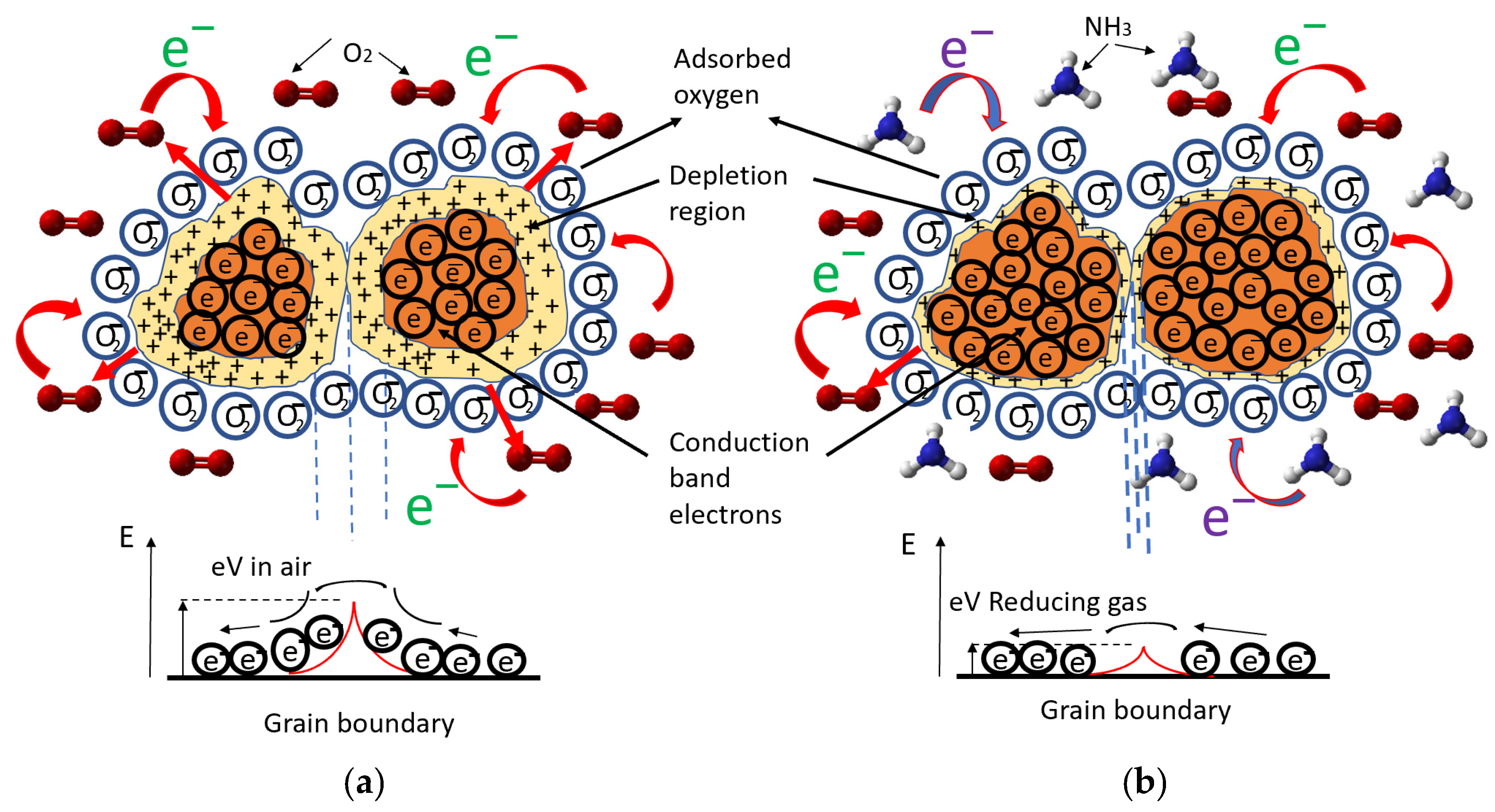
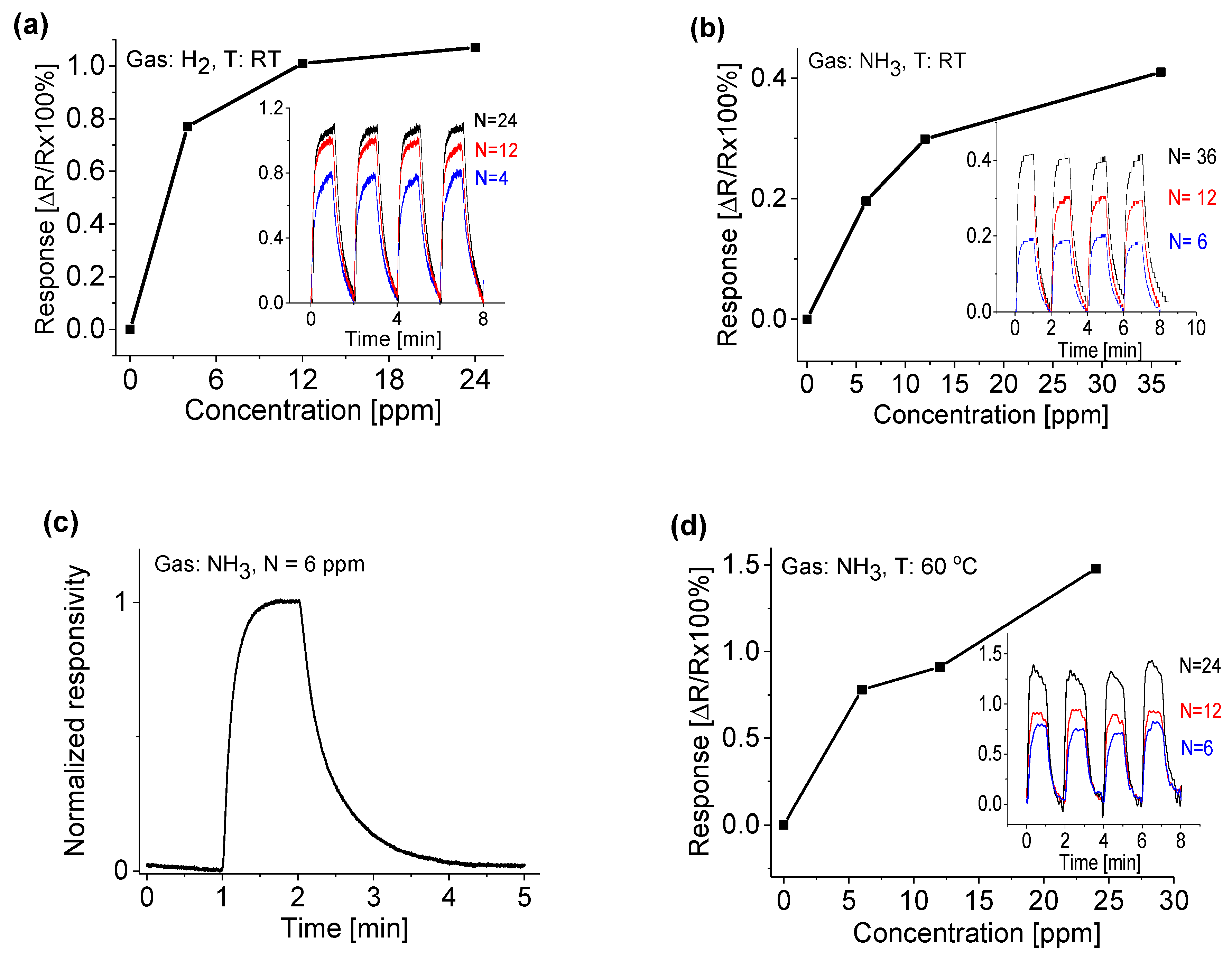
3.3. Response to Target Gases with Different Concentrations

Variation of electric properties of N-UNCD in air and H2 mentioned above suggested that gas sensing devices can be fabricated based on these nanomaterials, including hydrogen (H2) [31,32,33], methane (CH4) [19,34], carbon monoxide (CO) [20,35], ammonia [36,37], nitrogen dioxide (NO2) [34], and benzene (C6H6) and toluene (C7H8) [38]. In this paper, the test results corresponding to two types of molecules, H2, and NH3 gases, mixed with air gas, respectively, are reported. The test was conducted with the N-UNCD-based prototype placed into a closed chamber with a constant gas flow rate, where the valve was then switched to a target gas–air mixture. The gas concentrations in the chamber were controlled by adjusting gas flow rates.
As expected, the interaction between the gas molecules and the composites induces changes to the nanocomposites’ electrical and electronic properties, leading to a variation in the electrical conductivity of the sensing sample. The properties of gas sensing prototypes depend on the active layer’s surface reactions and the diffusion of analytes. To understand the basic mechanism, the response of the prototype is initially characterized in air (Figure 5a). The adsorption of the oxygen molecule at the surface withdraws electrons from the conduction band, leading to the formation of a thick depletion layer [39,40], resulting in a decrease of the conductivity or an increase of the resistance in the present n-type UNCD. When the UNCD prototype was exposed to NH3 gas, the adsorbed NH3 molecules would react with the adsorbed oxygen ions on the active layer and return electrons back to the UNCD [41,42]. This process reduces the depletion layer, hence increasing the electrical conductivity of UNCD, as shown in Figure 5b.
Figure 6a shows the basic data of cycling tests of sensing responses of the N-UNCD-based prototype toward H2 gas with three different concentrations at room temperature. When the target gas is turned on, the prototype responds to a conductivity rise at first and then reaches a stable state. After the target gas is turned off and pumped out, the prototype shows a quick conductivity decrease and then gradually recovers to its original state. The conductivity variation of the active layer is directly caused by the absorption of target gas molecules where the interaction between the external gas and the surface of composite through van der Waals forces is considered physisorption with a weak bond. The following definition of responsivity S
S = ΔR/Rair × 100%
is used to calculate the obtained relative response, where ΔR is the resistance change induced by the target gas, and Rair is the original resistance of the prototype in air. In general, the sensor response depends on many environmental parameters, such as the type of target gas, concentration, operating temperature, bias, and humidity. As shown in the inset of Figure 6a, the prototype has good repeatability and stability. Following an increase in H2 gas concentrations from 4 ppm up to 24 ppm, the yielded response strength increases slightly, despite the high concentration of target gas.
As a comparison, characterizations were also carried out with the N-UNCD prototype to NH3 gas with the gas concentration varying from 6 to 36 ppm. The obtained responsivities are 0.2, 0.3, and 0.41, respectively, as shown in Figure 6b. Comparing data from Figure 6a,b, two conclusions can be made: (1) the prototype has higher response strengths to hydrogen gas than that to ammonia gas, and (2) the prototype has shorter response times to ammonia gas than that to hydrogen gas at the same concentrations. In order to have precise measurements of response time and recovery time for a truly stable state response, a test with a longer cycle period was also carried out for N-UNCD based prototype to ammonia with a concentration of 6 ppm. As seen in Figure 6c, the rise time is less than 18 s. The rise time is defined as the time taken for the response signal to increase to 90% of the maximum value after the inlet of the target gas is turned on, whereas the recovery time is the time required for the signal amplitude to decrease to 10% of the maximum value after the inlet of the target gas is turned off. After the rise time, the response strength reached a very stable state with an excellent signal-to-noise ratio. The recovery time is slightly longer, around 64 s. Both values are significantly shorter than that of most commercial devices [43]. It was found that the obtained response time and recovery time remained nearly unchanged regardless of low or high concentrations of the target gas.
To understand the thermal effect on the gas sensing properties, the response at a high operating temperature was also evaluated. A heater was employed to change the temperature setting, while all other parameters remained unchanged. Figure 6d shows the response of the prototype at 60 °C and 1.0 V bias to NH3 gas with different concentrations ranging from 6 to 24 ppm. As seen in Figure 6b,d, the ammonia gas-induced response at 60 °C is nearly 3.5 times higher than that operating at room temperature. An increase in bias voltage from 1 to 2 V only resulted in increased response. It is anticipated that the high temperature enhances molecular gas dissociation on the surface of the sensing layer, thus improving catalytic activity. The target gas then reacts rapidly with agents presented on the surface, leading to an increase in sensitivity to temperature [44]. Good features, such as stable baseline, good repeatability, and low thermal noise strength, are evident from cycling tests, as shown in the Figure 6d inset. A high operating temperature does not however improve the response time and recovery time by much.
Although operating at a higher temperature will normally enhance the sensitivity of a gas sensor, it is a disadvantage for commercial use. Therefore, the properties of the present prototypes were characterized at different operating temperatures less than 100 °C. We completed all measurements at room temperature first and then at 60 °C. The same prototype was remeasured at room temperature and 60 °C, respectively, after the prototypes were kept in air for days, weeks, and months to test the long-term reproducibility. The prototypes appeared to have very good reproducibility at 60 °C, although short-term and long-term aging were not tested at a higher temperature.
As a comparison, the key performance parameters of pristine nanocarbon-based gas sensors published recently are listed in Table 1. Our N-UNCD film has the highest responsivity (lowest detectable concentration) of all reported gas sensors. Moreover, it has a much faster rise and decay time when responding to NH3 gas. Typically, the response time of the prototype is around 18 s and the recovery time is around 64 s at room temperature, which is much shorter than the gas sensing devices based on traditional semiconductors.

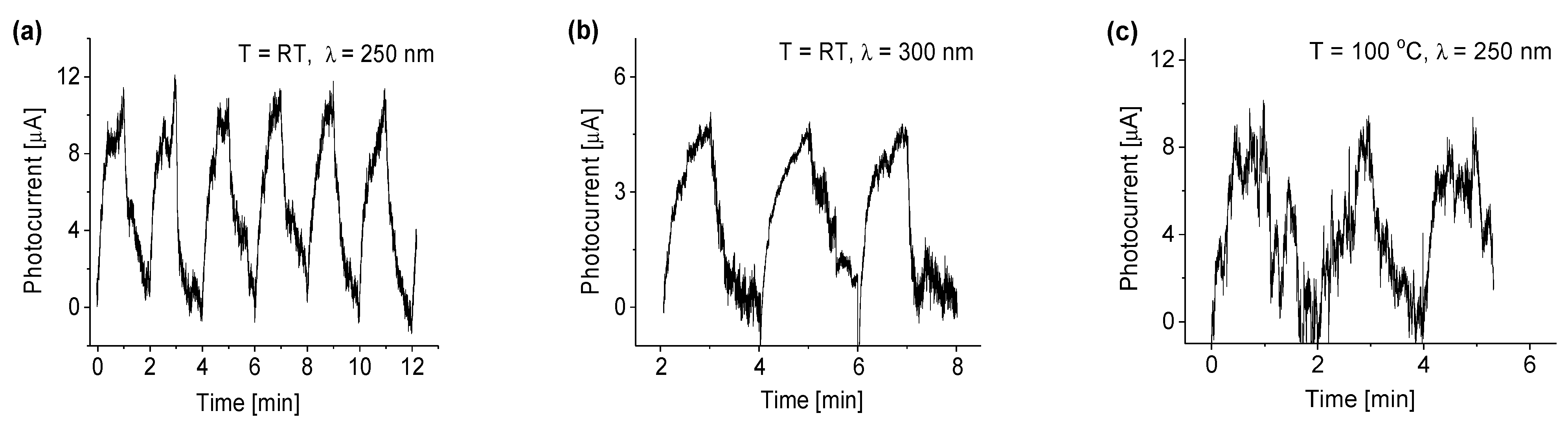
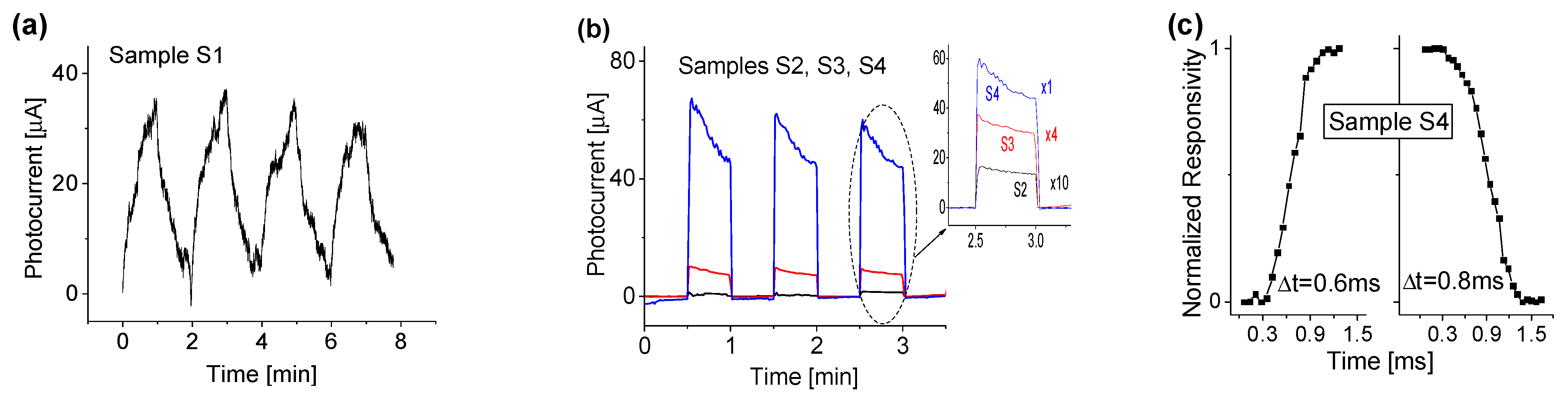
3.4. Response to Deep UV Illumination with Different Wavelengths

In addition to gas sensing properties, multifunctional N-UNCD also exhibits a high response to UV light illumination and different device structures have been demonstrated using synthetic diamond thin films of different morphologies [6,7,8,9,21,22,51,52,53,54,55,56,57,58,59,60,61,62]. Pen-Ray deep UV lamps (UVP, LLC) with wavelengths of 250 and 300 nm, respectively, were used as light sources for illuminations. The light intensity of UV lamps was around 1 mW/cm2 on the surface of the active layer and the exposed area of the active layer to UV light is around 2 mm2. When the prototype is exposed to UV light, the photonic energy of the UV light is absorbed, which excites the valence electrons, yielding photocurrent in the circuit.
The photocurrent obtained was mostly due to the majority charge carriers, which are free to flow through the ohmic contacts. However, this current was also connected to the presence of minority charge carriers. When minority carriers piled up at the contact, additional injection of majority charge carriers occurred until the minority carriers recombined. This effect leads to a large “photoconductive gain,” depending primarily on the ratio of the minority carrier lifetime to the majority carrier transit time, but the undesirable attributes are a relatively high dark current and a slow response time associated with a long carrier lifetime. Nevertheless, photoconductors are simple and useful for those applications where speed and dark current are not particularly important [63].
Figure 7a shows the typical response of N-UNCD-based prototypic UV photodetectors exposed to 250 nm UV light illumination with an intensity of 1 mW/cm2. The photocurrent variation following the light on–off cycles can be easily identified. The current could be directly attributed to the absorption of deep UV photons. Good features in repeatability and stability have been achieved in this prototype. The obtained maximum photocurrent was 11 μA and the dark current was 1 μA, yielding a signal-to-noise ratio of up to 11. Since the 250 nm light power on the active layer with an exposed area around 2 mm2 is 20 µW, the estimated responsivity Rλ = Iλ/Wλ (where Iλ is the induced photocurrent and Wλ is the total incident light power on the active layer of the porotype) is around 550 mA/W. This value is larger than a previously reported result obtained from UV photodetectors based on N-UNCD nanowires [64].
The response and recovery times, on the other hand, appear to be considerably long, up to 60 s, due to its intrinsic decay behavior towards the baseline. This behavior may be related to the multifactor nature of these phenomena. Nevertheless, a much higher photocurrent was obtained from the prototype when exposed to UV radiation. In general, there is a compromise between the photocurrent gain and the response speed for such a UV photodetector because a long minority carrier lifetime results in enhancements in not only photocurrent but also response time.
Two additional experiments were also carried out to examine the response of the prototype to long UV illumination and thermal effect. The first experiment shows that N-UNCD film-based prototype performed less effectively under 300 nm or longer UV light illumination, as shown in Figure 7b. When exposed to 300 nm light at the same intensity, the prototype yielded a photocurrent around 2.4 times less than that when exposed to 250 nm light, which indicates the fabricated N-UNCD prototype is less sensitive to a longer UV wavelength. This feature is attributed to the band structure and bandgap energy, which are the most important device parameters related to the electronic and optical properties of the nanostructured semiconductor. The result from the second experiment at an operating temperature of 100 °C is shown in Figure 7c. At a higher operating temperature, there were slight decreases in the photocurrent, baseline quality, and stability, as expected due to an increase in dark current and thermal noise.
It was found that a high bias would efficiently enhance the yield of induced photocurrent, as shown in Figure 8a, where a bias of 2 V was applied to the N-UNCD prototype. A slight increase in the bias from 1 V to 2 V resulted in a 3.2-fold increase in induced photocurrent (Figure 8a) compared to the data from Figure 7a. The N-UNCD prototype displays a clean, well-defined response and a stable baseline. However, both the long rise and recovery times are independent of the bias applied. A quick and strong response is witnessed from samples S2, S3, and S4 based prototypes. Figure 8b shows the responses of induced photocurrents from micro, submicron, and nanodiamond based prototypes exposed to 250 nm light illumination with an intensity of 1mW/cm2. A high signal-to-noise ratio of up to 90 was obtained.
The response strength or induced photocurrents highly relies on the quality of materials. The highest photocurrent up to 56 μA was obtained from sample S4. Correspondingly, its responsivity is up to 2750 mA/W, indicating the diamond film with large grain would be more suitable for UV photodetectors. The induced photocurrent was only 8.3 and 1.4 μA from samples S3 and S2, respectively.
To analyze the change in response time, a high-resolution Cobox interface was also used to remeasure the response time and recovery time. Typical results are shown in Figure 8c, from which the response time of the prototype can be estimated at around 0.6 ms and the recovery time is only 0.8 ms. It is expected that the actual response time and recovery time would be shorter. This is because time delay for reaching full intensity for UV lamps after switching on the lamp and florescence after switching off the lamp would affect the measurement results.

4. Conclusions

Although the fabrication was simple, fast, and cheap, the experiments demonstrated that the present multifunctional nanocomposites could respond to multiple external stimuli. The prototypes display excellent performance for quick response time, good response strength, stable baseline, and repeatability both in gas sensing and photo sensing measurements. The experimental data indicated that N-UNCD based prototype has a good selectivity in gas sensing. It was found that the response strength to H2 target gas is higher than that of NH3 gas at the same gas concentration. However, its responsivity is rather small to CH4, and almost no response to NO2. Its responsivity is better than any reported pristine nanocarbon based counterparts and response time is much short than the similar gas sensors based on traditional semiconductor and pristine nanocarbon materials.
In UV sensing characterization, an increase of applied bias from 1 V to 2 V would notably enhance N-UNCD-based prototype response strength/photocurrent from 11 to 35 μA and improve the signal-to-noise ratio. Whereas the rise of operating temperature up to 100 °C resulted in an increase in noise strength and a decrease of photocurrent from 11 μA to 8 μA. Both response and recovery times are long, up to 30 s, and independent of the bias applied. It was found that HFCVD fabrication of the other three diamond composite-based prototypes had a much faster response and recovery time. The shortest response time was 0.6 ms. The largest photocurrent from sample S4 reached 56 μA. The induced photocurrent was only 8.3 and 1.4 μA from the S3 and S2 samples, respectively, when exposed to the same UV illumination. It can be concluded that the diamond film with a larger grain would have higher responsivity for UV photodetector, suggesting that a fundamental trade-off among cost, photocurrent gain, and response speed of a photodetector is unavoidable. A long minority carrier lifetime would result in photocurrent enhancement, but increase the response time. It is important to reach a desirable balance among the sensitivity, response time and fabrication cost.
Finally, it should be mentioned that gas sensing properties of the N-UNCD film-based prototypes could possibly be enhanced significantly with UV illumination, as shown in our similar work with MoS2-based gas sensors [65]. It has been demonstrated that the light illuminated effectively shortened the response time and promoted the recovery rate of the MoS2-based gas sensor, which provided a strategy to design an optoelectronic device with optimal gas sensing properties. Next, we will investigate the possible combinations of UV light for improving the gas sensing properties of the N-UNCD material.

Author Contributions

Designing and performing the experiments, as well as analyzing the data and writing the manuscript, E.Y.L., A.F.Z. and P.X.F.; preparation of samples and data analysis, E.P. All authors have read and agreed to the published version of the manuscript.

Funding

NSF-CREST Center for Innovation, Research and Education in Environmental Nanotechnology (CIRE2N), grant HRD-1736093. Period: August 2017–August 2022.

Institutional Review Board Statement

Not applicable.

Informed Consent Statement

Not applicable.

Data Availability Statement

Not applicable.

Acknowledgments

This work was financially supported by the NSF-CREST Center for Innovation, Research and Education in Environmental Nanotechnology (CIRE2N), grant HRD-1736093. AFZ acknowledges the receipt of a IUP Senate Fellowship grant. The authors acknowledge partial assistance from R. Velazquez during the synthesis of diamond samples.

Conflicts of Interest

The authors declare no conflict of interest.

References

  1. El-Toni, A.M.; Habila, M.A.; Labis, J.P.; ALOthman, Z.A.; Alhoshan, M.; Elzatahry, A.A.; Zhang, F. Design, synthesis and applications of core–shell, hollow core, and nanorattle multifunctional nanostructures. Nanoscale 2016, 8, 2510–2531. [Google Scholar] [CrossRef] [PubMed]
  2. Quarta, A.; Di Corato, R.; Manna, L.; Argentiere, S.; Cingolani, R.; Barbarella, G.; Pellegrino, T. Multifunctional nanostructures based on inorganic nanoparticles and oligothiophenes and their exploitation for cellular studies. J. Am. Chem. Soc. 2008, 130, 10545–10555. [Google Scholar] [CrossRef]
  3. Tsao, J.Y.; Chowdhury, S.; Hollis, M.A.; Jena, D.; Johnson, N.M.; Jones, K.A.; Kaplar, R.J.; Rajan, S.; Van de Walle, C.G.; Bellotti, E.; et al. Ultrawide-Bandgap Semiconductors: Research Opportunities and Challenges. Adv. Electron. Mater. 2018, 4, 1600501. [Google Scholar] [CrossRef] [Green Version]
  4. Mokuno, Y.; Chayahara, A.; Yamada, H. Synthesis of large single crystal diamond plates by high rate homoepitaxial growth using microwave plasma CVD and lift-off process. Diam. Relat. Mater. 2008, 17, 415–418. [Google Scholar] [CrossRef]
  5. Sang, L.; Liao, M.; Sumiya, M. A comprehensive review of semiconductor ultraviolet photodetectors: From thin film to one-dimensional nanostructures. Sensors 2013, 13, 10482–10518. [Google Scholar] [CrossRef] [PubMed]
  6. Iwakaji, Y.; Kanasugi, M.; Maida, O.; Ito, T. Characterization of Diamond Ultraviolet Detectors Fabricated with High-Quality Singlecrystalline Chemical Vapor Deposition Films. Appl. Phys. Lett. 2009, 94, 223511. [Google Scholar] [CrossRef]
  7. Pace, E.; De Sio, A. Diamond detectors for space applications. Nucl. Instrum. Methods Phys. Res. A Accel. Spectrom. Detect. Assoc. Equip. 2003, 514, 93–99. [Google Scholar] [CrossRef]
  8. Lin, C.R.; Wei, D.H.; BenDao, M.K.; Chen, W.E.; Liu, T.Y. Development of High-Performance UV Detector Using Nanocrystalline Diamond Thin Film. Int. J. Photoenergy 2014, 2014, 492152. [Google Scholar] [CrossRef] [Green Version]
  9. Tang, K.; Wang, L.J.; Huang, J.; Ma, Y.; Hu, G.; Zhu, X.F.; Xia, Y.B. Diamond film ultraviolet detectors with different diamond grain size. J. Phys. Conf. Ser. 2009, 152, 012015. [Google Scholar] [CrossRef] [Green Version]
  10. Tallaire, A.; Achard, J.; Silva, F.; Brinza, O.; Gicquel, A. Growth of large size diamond single crystals by plasma assisted chemical vapour deposition: Recent achievements and remaining challenges. C. R. Phys. 2013, 14, 169–184. [Google Scholar] [CrossRef]
  11. Soleimanzadeh, R.; Naamoun, M.; Floriduz, A.; Khadar, R.A.; van Erp, R.; Matioli, E. Seed Dibbling Method for the Growth of High-Quality Diamond on GaN. ACS Appl. Mater. Interfaces 2021, 13, 43516–43523. [Google Scholar] [CrossRef] [PubMed]
  12. Kim, M.S.; Jang, T.H.; Gwon, J.U.; Kim, T.G.; Bae, M.K. Nitrogen-doping effect on single-crystal diamond synthesis by HFCVD. Int. J. Mod. Phys. B 2022, 36, 2242019. [Google Scholar] [CrossRef]
  13. Butler, J.E.; Windischmann, H. Developments in CVD-diamond synthesis during the past decade. MRS Bull. 1998, 23, 22–27. [Google Scholar] [CrossRef]
  14. Zhou, A.F.; Wang, X.; Pacheco, E.; Feng, P.X. Ultrananocrystalline Diamond Nanowires: Fabrication, Characterization, and Sensor Applications. Materials 2021, 14, 661. [Google Scholar] [CrossRef]
  15. Salgado-Meza, M.; Martínez-Rodríguez, G.; Tirado-Cantú, P.; Montijo-Valenzuela, E.E.; García-Gutiérrez, R. Synthesis and properties of electrically conductive/nitrogen grain boundaries incorporated ultrananocrystalline diamond (N-uncd) thin films grown by microwave plasma chemical vapor deposition (mpcvd). Appl. Sci. 2021, 11, 8443. [Google Scholar] [CrossRef]
  16. Auciello, O.; Sumant, A.V. Status review of the science and technology of ultrananocrystalline diamond (UNCD™) films and application to multifunctional devices. Diam. Relat. Mater. 2010, 19, 699–718. [Google Scholar] [CrossRef]
  17. Krauss, A.R.; Auciello, O.; Gruen, D.M.; Jayatissa, A.; Sumant, A.; Tucek, J.; Mancini, D.C.; Moldovan, N.; Erdemir, A.; Ersoy, D.; et al. Ultrananocrystalline diamond thin films for MEMS and moving mechanical assembly devices. Diam. Relat. Mater. 2001, 10, 1952–1961. [Google Scholar] [CrossRef]
  18. Zhou, A.F.; Pacheco, E.; Zhou, B.; Feng, P.X. Size-Dependent Electrical Transport Properties in Conducting Diamond Nanostripes. Nanomaterials 2021, 11, 1765. [Google Scholar] [CrossRef]
  19. Feng, P.; Wang, X.; Aldalbahi, A.; Zhou, A.F. Methane induced electrical property change of nitrogen doped ultrananocrystalline diamond nanowires. Appl. Phys. Lett. 2015, 107, 233103. [Google Scholar] [CrossRef]
  20. Peng, X.; Li, Y.; Duan, S.; Chu, J.; Feng, P. Precise B-doped ultrananocrystalline diamond nanowire arrays for high performance of CO gas sensor. Mater. Lett. 2020, 265, 127404. [Google Scholar] [CrossRef]
  21. Velázquez, R.; Rivera, M.; Zhou, A.F.; Bromley, D.; Feng, P.X. Zero Bias, Super Sensitive and Broadband UV Photoconductor Based on Pt Nanoparticle Functionalized Ultrananocrystalline Diamond Nanowire Arrays. Def. Syst. Inf. Anal. Cent. (DSIAC) J. 2019, 6, 15. [Google Scholar]
  22. Zhou, A.F.; Velázquez, R.; Wang, X.; Feng, P.X. Nanoplasmonic 1D Diamond UV Photodetectors with High Performance. ACS Appl. Mater. Interfaces 2019, 11, 38068–38074. [Google Scholar] [CrossRef]
  23. Wang, X. Synthesis, Fabrication, Characterization and Application of Ultrananocrystalline Diamond Micro- and Nanosctructures. Ph.D. Thesis, University of Puerto Rico, San Juan, Puerto Rico, 2012. [Google Scholar]
  24. Williams, O.A.; Zimmermann, T.; Kubovic, M.; Denisenko, A.; Kohn, E.; Jackman, R.B.; Gruen, D.M. Synthesis, Properties and Applications of Ultrananocrystalline Diamond; Gruen, D.M., Shenderova, O.A., Vul, A.Y., Eds.; Springer: Dordrecht, The Netherlands, 2005; pp. 373–382. [Google Scholar]
  25. Wang, X.; Ocola, L.E.; Divan, R.S.; Sumant, A.V. Nanopatterning of ultrananocrystalline diamond nanowires. Nanotechnology 2012, 23, 075301. [Google Scholar] [CrossRef] [PubMed]
  26. Ali, M.; Ürgen, M. Surface morphology, growth rate and quality of diamond films synthesized in hot filament CVD system under various methane concentrations. Appl. Surf. Sci. 2011, 257, 8420–8426. [Google Scholar] [CrossRef]
  27. Birrell, J.; Gerbi, J.E.; Auciello, O.; Gibson, J.M.; Johnson, J.; Carlisle, J.A. Interpretation of the Raman spectra of ultrananocrystalline diamond. Diam. Relat. Mater. 2005, 14, 86–92. [Google Scholar] [CrossRef]
  28. Williams, O.A.; Daenen, M.; D’Haen, J.; Haenen, K.; Maes, J.; Moshchalkov, V.V.; Nesládek, M.; Gruen, D.M. Comparison of the growth and properties of ultrananocrystalline diamond and nanocrystalline diamond. Diam. Relat. Mater. 2006, 15, 654–658. [Google Scholar] [CrossRef]
  29. Li, Y.; Xia, Y.; Liu, K.; Ye, K.; Wang, Q.; Zhang, S.; Huang, Y.; Liu, H. Constructing Fe-MOF-derived Z-scheme photocatalysts with enhanced charge transport: Nanointerface and carbon sheath synergistic effect. ACS Appl. Mater. Interfaces 2020, 12, 25494–25502. [Google Scholar] [CrossRef]
  30. Wang, Y.; Chen, D.; Zhang, J.; Balogun, M.S.; Wang, P.; Tong, Y.; Huang, Y. Charge Relays via Dual Carbon-Actions on Nanostructured BiVO4 for High Performance Photoelectrochemical Water Splitting. Adv. Funct. Mater. 2022, 32, 2112738. [Google Scholar] [CrossRef]
  31. Kang, W.P.; Gurbuz, Y.; Davidson, J.L.; Kerns, D.V. A New Hydrogen Sensor Using a Polycrystalline Diamond-Based Schottky Diode. J. Electrochem. Soc. 1994, 141, 2231. [Google Scholar] [CrossRef]
  32. Kang, W.P.; Gurbuz, Y.; Davidson, J.L.; Kerns, D.V. A polycrystalline diamond thin-film-based hydrogen sensor. Sens. Actuators B Chem. 1995, 25, 421–425. [Google Scholar] [CrossRef]
  33. Gurbuz, Y.; Kang, W.P.; Davidson, J.L.; Kerns, D.V. Analyzing the mechanism of hydrogen adsorption effects on diamond based MIS hydrogen sensors. Sens. Actuators B Chem. 1996, 35, 68–72. [Google Scholar] [CrossRef]
  34. Zhou, A.F.; Wang, X.; Feng, X.P. Nitrogen-doped Diamond Nanowire Gas Sensor for the Detection of Methane. Adv. Mater. Lett. 2020, 11, 20021473. [Google Scholar] [CrossRef]
  35. Peng, X.Y.; Chu, J.; Wang, L.D.; Duan, S.; Feng, P. Boron-doped diamond nanowires for CO gas sensing application. Sens. Actuators B Chem. 2017, 241, 383–389. [Google Scholar] [CrossRef] [Green Version]
  36. Davydova, M.; Kulha, P.; Laposa, A.; Hruska, K.; Demo, P.; Kromka, A. Gas sensing properties of nanocrystalline diamond at room temperature. Beilstein. J. Nanotechnol. 2014, 5, 2339–2345. [Google Scholar] [CrossRef] [Green Version]
  37. Kočí, M.; Kromka, A.; Bouřa, A.; Szabó, O.; Husák, M. Hydrogen-Terminated Diamond Surface as a Gas Sensor: A Comparative Study of Its Sensitivities. Sensors 2021, 21, 5390. [Google Scholar] [CrossRef]
  38. Gurbuz, Y.; Kang, W.P.; Davidson, J.L.; Kerns, D.V. Diamond microelectronic gas sensor for detection of benzene and toluene. Sens. Actuators B Chem. 2004, 99, 207–215. [Google Scholar] [CrossRef]
  39. Sharma, N.; Sharma, N.; Srinivasan, P.; Kumar, S.; Balaguru Rayappan, J.B.; Kailasam, K. Heptazine based organic framework asa chemiresistive sensor for ammonia detection atroom temperature. J. Mater. Chem. A 2018, 6, 18389–18395. [Google Scholar] [CrossRef]
  40. Wang, C.; Yin, L.; Zhang, L.; Xiang, D.; Gao, R. Metal Oxide Gas Sensors: Sensitivity and Influencing Factors. Sensors 2010, 10, 2088–2106. [Google Scholar] [CrossRef] [Green Version]
  41. Khun Khun, K.; Mahajan, A.; Bedi, R.K. SnO2 thick films for room temperature gas sensing applications. J. Appl. Phys. 2009, 106, 124509. [Google Scholar] [CrossRef]
  42. Gu, D.; Li, X.; Wang, H.; Li, M.; Xi, Y.; Chen, Y.; Wang, J.; Rumyntseva, M.N.; Gaskov, A.M. Light enhanced VOCs sensing of WS2 microflakes based chemiresistive sensors powered by triboelectronic nangenerators. Sens. Actuators B Chem. 2018, 256, 992–1000. [Google Scholar] [CrossRef]
  43. Timmer, B.; Olthuis, W.; Van Den Berg, A. Ammonia sensors and their applications—A review. Sens. Actuators B Chem. 2005, 107, 666–677. [Google Scholar] [CrossRef]
  44. Davydova, M.; Stuchlik, M.; Rezek, B.; Kromka, A. Temperature enhanced gas sensing properties of diamond films. Vacuum 2012, 86, 599–602. [Google Scholar] [CrossRef]
  45. Lu, G.; Ocola, L.E.; Chen, J. Reduced graphene oxide for room-temperature gas sensors. Nanotechnology 2009, 20, 445502. [Google Scholar] [CrossRef] [PubMed]
  46. Mao, S.; Lu, G.; Chen, J. Nanocarbon-based gas sensors: Progress and challenges. J. Mater. Chem. A 2014, 2, 5573–5579. [Google Scholar] [CrossRef] [Green Version]
  47. Niu, F.; Tao, L.M.; Deng, Y.C.; Wang, Q.H.; Song, W.G. Phosphorus doped graphene nanosheets for room temperature NH3 sensing. New J. Chem. 2014, 38, 2269–2272. [Google Scholar] [CrossRef]
  48. Suehiro, J.; Zhou, G.; Hara, M. Fabrication of a carbon nanotube-based gas sensor using dielectrophoresis and its application for ammonia detection by impedance spectroscopy. J. Phys. D Appl. Phys. 2003, 36, L109. [Google Scholar] [CrossRef]
  49. Travlou, N.A.; Seredych, M.; Rodríguez-Castellón, E.; Bandosz, T.J. Activated carbon-based gas sensors: Effects of surface features on the sensing mechanism. J. Mater. Chem. A 2015, 3, 3821–3831. [Google Scholar] [CrossRef]
  50. Moncea, O.; Casanova-Chafer, J.; Poinsot, D.; Ochmann, L.; Mboyi, C.D.; Nasrallah, H.O.; Llobet, E.; Makni, I.; El Atrous, M.; Brandès, S.; et al. Diamondoid Nanostructures as sp3-Carbon-Based Gas Sensors. Angew. Chem. Int. Ed. Engl. 2019, 58, 9933–9938. [Google Scholar] [CrossRef] [Green Version]
  51. Mendoza, F.; Makarov, V.; Weiner, B.; Morell, G. Solar-Blind Field-Emission Diamond Ultraviolet Detector. Appl. Phys. Lett. 2015, 107, 201605. [Google Scholar] [CrossRef] [Green Version]
  52. Balducci, A.; Marinellia, M.; Milani, E.; Morgada, M.E.; Tucciarone, A.; Verona-Rinati, G. Extreme Ultraviolet Single-Crystal Diamond Detectors by Chemical Vapor Deposition. Appl. Phys. Lett. 2005, 86, 193509. [Google Scholar] [CrossRef]
  53. Teraji, T.; Yoshizaki, S.; Wada, H.; Hamada, M.; Ito, T. Highly Sensitive UV Photodetectors Fabricated Using High-Quality Single-Crystalline CVD Diamond Films. Diam. Relat. Mat. 2004, 13, 858–862. [Google Scholar] [CrossRef]
  54. Liao, M.; Wang, X.; Teraji, T.; Koizumi, S.; Koide, Y. Light Intensity Dependence of Photocurrent Gain in Single-Crystal Diamond Detectors. Phys. Rev. B 2010, 81, 033304. [Google Scholar] [CrossRef]
  55. Liu, K.; Liu, B.; Zhao, J.; Shu, G.; Xu, X.; Yao, K.; Sun, M.; Zhang, X.; Yang, Y.; Su, Z.; et al. Application of back bias to interdigital-electrode structured diamond UV detector showing enhanced responsivity. Sens. Actuator A Phys. 2019, 290, 222–227. [Google Scholar] [CrossRef]
  56. McKeag, R.D.; Chan, S.M.; Jackman, R.B. Polycrystalline Diamond Photoconductive Device with High UV-Visible Discrimination. Appl. Phys. Lett. 1995, 67, 2117–2119. [Google Scholar] [CrossRef]
  57. Shi, X.; Yang, Z.; Yin, S.; Zeng, H. Al Plasmon-Enhanced Diamond Solar-Blind UV Photodetector by Coupling of Plasmon and Excitons. Mater. Technol. 2016, 31, 544–547. [Google Scholar] [CrossRef]
  58. BenMoussa, A.; Soltani, A.; Haenen, K.; Kroth, U.; Mortet, V.; Barkad, H.A.; Bolsee, D.; Hermans, C.; Richter, M.; De Jaeger, J.C.; et al. New Developments on Diamond Photodetector for VUV Solar Observations. Semicond. Sci. Technol. 2008, 23, 035026. [Google Scholar] [CrossRef]
  59. Lin, C.N.; Lu, Y.J.; Yang, X.; Tian, Y.Z.; Gao, C.J.; Sun, J.L.; Dong, L.; Zhang, F.; Hu, W.D.; Shan, C.X. Diamond-Based All-Carbon Photodetectors for Solar-Blind Imaging. Adv. Opt. Mater. 2018, 6, 1800068. [Google Scholar] [CrossRef]
  60. Koide, Y.; Liao, M.; Alvarez, J. Thermally stable solar-blind diamond UV photodetector. Diam. Relat. Mater. 2006, 15, 1962–1966. [Google Scholar] [CrossRef]
  61. Wang, L.; Chen, X.; Wu, G.; Guo, W.; Wang, Y.; Cao, S.; Shang, K.; Han, W. Study on trapping center and trapping effect in MSM ultraviolet photo-detector on microcrystalline diamond film. Phys. Status Solidi 2010, 207, 468–473. [Google Scholar] [CrossRef]
  62. Salvatori, S.; Scotti, F.; Conte, G.; Rossi, M.C. Diamond-based UV photodetectors for high temperature applications. Electron. Lett. 1999, 35, 1768–1770. [Google Scholar] [CrossRef]
  63. Schühle, U.; Hochedez, J.F. Solar-blind UV detectors based on wide band gap semiconductors. In Observing Photons in Space; Springer: New York, NY, USA, 2003; pp. 467–477. [Google Scholar]
  64. Pacheco, E.; Zhou, B.; Aldalbahi, A.; Zhou, A.F.; Feng, P.X. Zero-biased and visible-blind UV photodetectors based on nitrogen-doped ultrananocrystalline diamond nanowires. Ceram. Int. 2022, 48, 3757–3761. [Google Scholar] [CrossRef]
  65. Peng, X.; Han, Y.; Zhang, Q.; Feng, P.; Jia, P.; Cui, H.; Wang, L.; Duan, S. Performance Improvement of MoS2; Gas Sensor at Room Temperature. IEEE Trans. Electron Devices 2021, 68, 4644–4650. [Google Scholar] [CrossRef]
Figure 1. (a) SEM image of sample S1 (scale bar = 0.5 μm). (b) A 2.5 μm × 2.5 μm AFM image of S1. The average grain size is around 3–5 nm in diameter. (c) SEM image of sample S2 (scale bar = 0.5 μm). (d) SEM image of sample S3 (scale bar = 0.5 μm). (e) SEM image of sample S4 (scale bar = 5 μm).
Chemosensors 10 00488 g001
Figure 2. Raman spectra of samples (a) S1, (b) S2, (c) S3, and (d) S4.
Chemosensors 10 00488 g002
Figure 3. Schematics of the (a) structure of prototypes and (b) homemade characterization station.
Chemosensors 10 00488 g003
Figure 4. I–V properties of S1–S4 samples in (a) open air at room temperature, (b) open air, and (c) H2 at 25 (RT), 60, and 120 °C. Inset: the calculated resistances. (d) The measured resistances of samples S1–S4 in open air at room temperature to 200 °C.
Chemosensors 10 00488 g004
Figure 5. The scheme for physisorption under reducing gas of (a) air and (b) NH3.
Chemosensors 10 00488 g005
Figure 6. The response strengths of the prototype to (a) H2, (b) ammonia gas at room temperature, (c) as a function of time, and (d) at 60 °C. The bias of 1 V remained unchanged for all cases. Inset: the response as a function of time at different concentrations (N) in ppm.
Chemosensors 10 00488 g006
Figure 7. N-UNCD UV responses to (a) 250 nm, (b) 300 nm when the sensor was operated at room temperature, and (c) 250 nm operated at 100 °C. The bias of 1 V and light intensity of 1 mW/cm2 remained unchanged for all cases.
Chemosensors 10 00488 g007
Figure 8. UV response of samples (a) S1 and (b) S2–S4 based prototypes at a bias of 2 V and room temperature. (c) Normalized time response of sample S4.
Chemosensors 10 00488 g008
Table 1. Comparison of the performance on gas sensing of the recently published pristine nanocarbon based materials.
Pristine Nanocarbon
Materials
Detected Gas MoleculesResponsivity and
Operating Temperature
Response TimeRecover TimeReference
Graphene (rGO)H24.5% (160 ppm)20 s10 s[45]
UNCD nanowire (Boron doping)H220% (100 ppm)
at 400 °C
--[35]
Graphene film (CVD)NH390% (1000 ppm)
at 200 °C
180 min-[46]
Pristine graphene (PG) (P-doping)NH35.4% (100 ppm)2.23 min13.6 min[47]
Multiwalled
carbon nanotubes (MWCNTs)
NH310 ppm~100 s-[48]
Wood-based activated carbonNH3100–500 ppm--[49]
Diamondoid Nanostructures (H2P-DiamOH)NH36% (25 ppm)
at 100 °C
~10 min~40 min[50]
N-UNCD filmH20.084% per ppm at room temperature (RT)20 s>64 sThis work
NH30.02% per ppm at room temperature (RT)18 s~64 sThis work
NH30.07% per ppm
at 60 °C
16 s>64 sThis work
Publisher’s Note: MDPI stays neutral with regard to jurisdictional claims in published maps and institutional affiliations.

