Article

A Novel ON-State Resistance Modeling Technique for MOSFET Power Switches

by
Ionuț-Constantin Guran
*,
Adriana Florescu
and
Lucian Andrei Perișoară
Department of Applied Electronics and Information Engineering, Faculty of Electronics, Telecommunications and Information Technology, University Politehnica of Bucharest, 060042 Bucharest, Romania
*
Author to whom correspondence should be addressed.
Mathematics 2023, 11(1), 72; https://doi.org/10.3390/math11010072
Submission received: 24 November 2022 / Revised: 13 December 2022 / Accepted: 21 December 2022 / Published: 25 December 2022

Abstract

:
Nowadays, electronic circuits’ time to market is essential, with engineers trying to reduce it as much as possible. Due to this, simulation has become the main testing concept used in the electronics domain. In order to perform the simulation of a circuit, a behavioral model must be created. Metal-Oxide-Semiconductor Field-Effect Transistors (MOSFETs) are semiconductor devices found in a multitude of electronic circuits, and they are also used as power switches in many applications, such as low-dropout linear voltage regulators, switching regulators, gate drivers, battery management systems, etc. A MOSFETs’ behavior is extremely complex to model, thus, creating high-performance models for these transistors is an imperative condition in order to emulate the exact real behavior of a circuit using them. An essential parameter of MOSFET power switches is the ON-state resistance (RDSON), because it determines the power losses during the ON state. Ideally, the power losses need to be zero. RDSON depends on multiple factors, such as temperature, load current, and gate-to-source voltage. Previous studies in this domain focus on the modeling of the MOSFET only in specific operating points, but do not cover the entire variation range of the parameters, which is critical for some applications. For this reason, in this paper, there was introduced for the first time a novel ON-state resistance modeling technique for MOSFET Power Switches, which solves the entire RDSON dependency on the transistor’s variables stated above. The novel RDSON modeling technique is based on modulating the transistor’s gate-to-source voltage such that the exact RDSON value is obtained in each possible operating point. The method was tested as a real-life example by creating a behavioral model for an N-channel MOSFET transistor and the chosen simulation environment was Oregon, USA, Computer-Aided Design (OrCAD) capture. The results show that the model is able to match the transistor’s RDSON characteristics with a maximum error of 0.8%. This is extremely important for applications in which the temperatures, voltages, and currents vary over a wide range. The new proposed modeling method covers a gap in the behavioral modeling domain, due to the fact that, until now, it was not possible to model the RDSON characteristics in all operating corners.

1. Introduction

Power electronics is a domain in which the power switches play a key role and employs the use of a multitude of silicon devices, such as diodes, thyristors, bipolar junction transistors (BJT), and unipolar transistors: junction-gate field-effect transistor (JFET) and MOSFET transistor [1,2]. BJTs are easy to manufacture and imply low costs, but the driver circuits are more complicated and lead to increased costs in the end [2]. Due to their reduced-complexity gate driving circuits, high switching speed, high input impedance, and good thermal stability, MOSFET transistors have become, today, one of the main semiconductor devices used as power switches in power electronic circuits [3].
The power levels required by the applications used in power electronics are spread over a large spectrum, as shown in Figure 1. The first category is represented by the applications that use low current levels (around 1A), such as display drives. The second category includes devices that use a small supply voltage (less than 100 V). Automotive electronics and power supplies used in computers represent some examples within this category. The most suitable power device here is the silicon power MOSFET due to its fast switching time and low ON-state resistance. The third category is represented by power devices that use high operating voltages (more than 200 V). Consumer appliances, electric vehicle drives, and lamp ballasts are some typical examples for this category [4]. Considering the previous information, it is generally accepted that any switch that can pass a minimum current of 1 A is a power switch [5].
Simulation has become the main testing concept used in the electronics domain because it reduces the testing costs, duration, and can reveal faults and flaws in the design process or validate the correct functioning of the system. A behavioral model is a software file written in a specific simulation language, which emulates the real behavior of a circuit. However, accurate behavioral models are needed for the circuits to be tested, such that the simulated behavior corresponds to the real behavior. One of the most important electronic circuits simulators is PSpice, which can be used for the simulation of a wide range of analog and digital applications. PSpice includes analog and digital libraries of standard components and also emulates multimeters, oscilloscopes, signal generators, and frequency spectrum analyzers [6,7].
In MOSFET power switches, the drain-source ON-state resistance (RDSON) is a key parameter, which greatly varies with the junction temperature TJ and with the gate-to-source voltage VGS [8]. Stefanskyi et al. [9] made a comparison between four power MOSFET Simulation Program with Integrated Circuit and Phases (SPICE) models provided by main transistor manufacturers and they reveal that each model is created by using Analog Behavioral Modeling (ABM) sources that create complex structures, but none of the models can be easily customized by external users. Moreover, the results show that the model characteristics do not accurately match the datasheet ones. However, the models were only tested at a junction temperature TJ of 25 °C and only the drain current vs. drain-source voltage characteristics are provided and, hence, no RDSON variation analysis was performed. Pratap et al. [1] proposed a simplified SPICE model for a power MOSFET. Their approach is the reuse of the available built-in MOSFET SPICE model, to which they add a series voltage source on the transistor gate and a parallel current source to the transistor drain-source channel for temperature compensation. Only the drain current vs. drain-source voltage characteristics are simulated and compared to the datasheet characteristics. The results show a very close match. However, only a temperature of 25 °C is used so that the RDSON variation cannot be interpreted. He et al. [10] introduced an approach to the generation of corner and statistical models limited to Silicon Carbide (SiC) MOSFETs. The method is able to produce good results, but the temperature effects are not taken into account. In addition, it was tested only for a finite set of RDSON values. Hsu et al. [11] presented a simple SPICE modeling method for SiC MOSFETs, which is based on mathematical equations and also uses a diode along with a JFET transistor. The method accounts for the RDSON variation with the gate voltage and obtains good fitting results compared to the conventional manufactures’ approach. Further, the RDSON variation with the junction temperature is studied but only in a finite number of points without giving clear results on the fitting error. Borghese et al. [12] described a compact electrothermal SPICE model for a SiC MOSFET that can be also used for other MOSFET types. The method uses only a small set of parameters to fit the MOSFET performance. The simulated drain current vs. drain-source voltage and drain current vs. gate-source voltage are compared with the datasheet characteristics and the results show a very good match. This analysis is conducted only for two junction temperatures, 25 °C and 125 °C; hence, the RDSON variation over temperature cannot be determined. For this reason, the paper puts forward a novel method of modeling the ON-state resistance of MOSFET power switches that studies and covers the entire RDSON variation range given in the datasheet.
The main contributions of this paper are listed below:
  • Simulation of the existing model of CSD13380F3 N-channel MOSFET transistor from Texas Instruments and plotting its RDSON characteristics;
  • Implementation of a new model for CSD13380F3 N-channel MOSFET transistor using the novel method, which focuses on the RDSON characteristics, as listed in the datasheet;
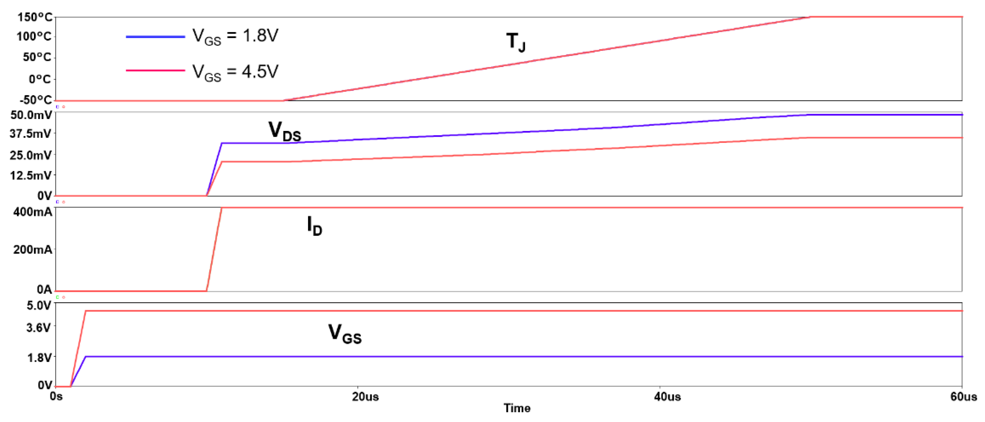
  • Implementation of an external temperature pin that allows one to emulate the self-heating effect of the transistor;
  • Simulation of the new CSD13380F3 model using OrCAD Capture environment and PSpice Allegro simulator;
  • Comparison between the existing model and the new model from the achieved performance point of view;
  • The simulation results based on the novel RDSON modeling technique show that it is possible to model the transistor RDSON in all operating corners accurately;
  • Using this novel method, the switching behavior of the MOSFET power switch model is able to match the real-life characteristics of the component over the entire operating range, not only in discrete operating points;
  • Highly reliable MOSFET power switch models can be built using the new RDSON modeling technique in a fast and efficient manner, only by defining the theoretical RDSON characteristics and without having to set other parameters.
The remainder of this paper is organized as follows: Section 2 reveals the background related to MOSFET RDSON, Section 3 presents the existing CSD13380F3 transistor model designed by Texas Instruments and the simulation of its RDSON characteristics, Section 4 shows materials and methods for the new transistor model implementation, Section 5 presents the simulation results for the new model, Section 6 comprises a comparison between the existing model from Texas Instruments and the new proposed model, and finally, the conclusions are presented in Section 7.

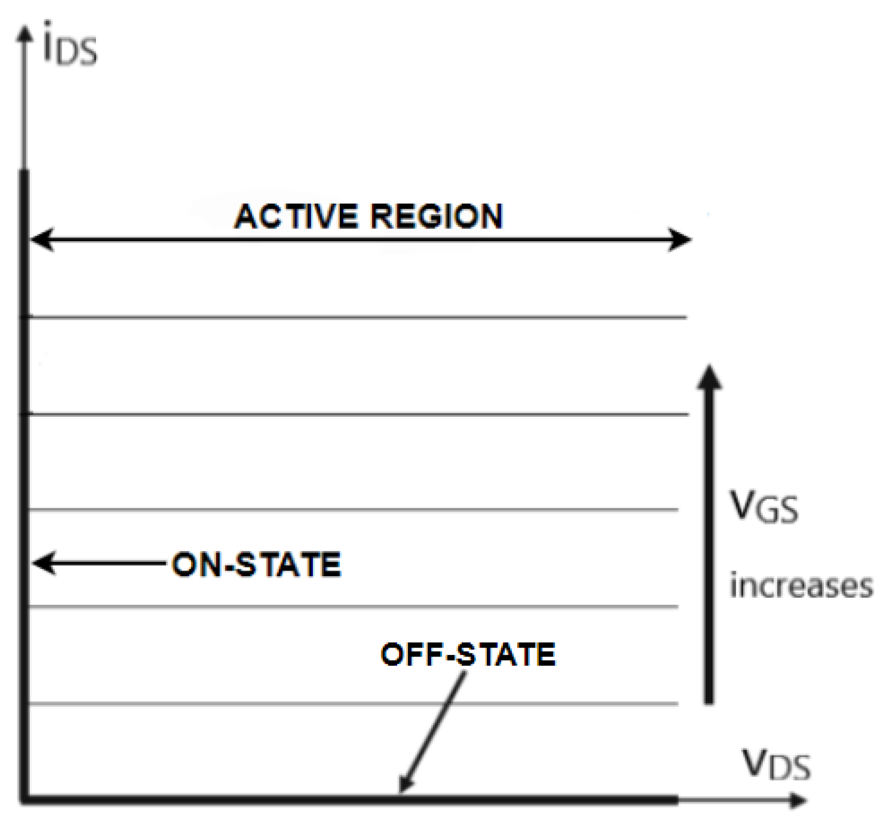
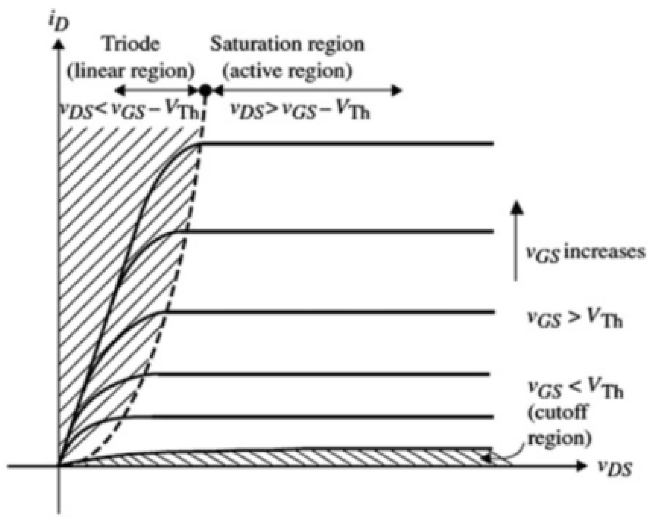
2. Background of the MOSFET Used as Power Switch

The selection of the most appropriate device for a certain application is a difficult task for an engineer, since it requires knowledge about the characteristics of the device and its unique features. Compared to low-power devices, power devices present a more complex structure and Operational current vs. Voltage characteristics. Moreover, the transistor driver design sees an increase in complexity [13].
The MOSFET transistor symbols are shown in Figure 2. Each MOSFET has a gate (G), drain (D), and source (S) terminals. There is also a fourth terminal, but it is usually connected internally to the source in power MOSFETs, so that is why it is omitted in some symbols. There are two main MOSFET transistor types: N-channel, where the drain current iD flows from D to S, and P-channel, where iD flows from S to D. For each channel, there are two other transistor types: depletion and enhancement MOSFETs, depending on the barrier layer used [14,15,16].
Figure 3 presents the ideal MOSFET power switch drain current vs. drain-source voltage family of characteristics iDS(vDS) at increasing gate voltages vGS as a parameter. The ideal MOSFET power switch is able to conduct current in the ON state with a zero-voltage drop and has no leakage current during the OFF state when it blocks the voltage. In the active region, the ideal MOSFET power switch can operate at high current (iDS) and voltage (vDS). The characteristics are uniformly spaced in the active region, indicating that the gain is independent of the iDS and vDS [4,13].
The iD(vDS) family of characteristics of a real MOSFET power switch is shown in Figure 4. The real power switch is characterized by a finite ON-state resistance RDSON in the linear region, as well as a finite leakage current in the OFF state (cutoff region). The iD(vDS) characteristics are not uniformly spaced in the active region due to the square law dependency on the gate voltage vGS. The iD dependency on the vDS voltage in the active region (also known as channel length modulation) is not shown here [4,5,13].
One of the key parameters of a MOSFET power switch is the drain-source ON-state resistance (RDSON). When the power MOSFET is in the linear region, the device behaves like a constant resistance, which is linearly proportional to the change between the drain-source voltage vDS and the drain current iD, at a constant gate-source voltage VGS and at a constant junction temperature TJ [2,8,13]:
R D S O N = v D S i D | V G S , T J = c o n s t a n t  
The RDSON value has a great significance and can vary between tens of milliohms for low-voltage MOSFETs and a few ohms for high-voltage MOSFETs. The importance of RDSON lies in determining the forward voltage drop across the transistors and the power losses during the ON state (PON,LOSS). For a constant drain current ID, the power losses are computed as shown [2,8,17]:
P O N , L O S S = I D 2 · R D S O N
N-channel, enhancement type is the most used MOSFET switch in the power electronics domain. The drain current iD starts flowing when a channel between the drain and the source is established. The channel creation occurs when the gate-source voltage exceeds the transistor threshold voltage VT. The power MOSFET operates in the cutoff region when the gate-source voltage is lower than the threshold voltage, vGS < VT; hence, no channel is induced and only a leakage current iLEAK flows. For vGS > VT, the MOSFET can operate either in the linear region (triode region) or in the saturation region, depending on the value of the drain-source voltage vDS. For the linear region of operation, the conditions are: vDS < vGS − VT and vGS > VT. For the saturation region, the following conditions apply: vDS > vGS − VT and vGS > VT. In the linear region, the channel is continuous, having no pinch-off and this results in the drain current iD being proportional to the channel resistance. In the saturation, the channel pinches off and a constant-drain current ID results. When vGS exceeds VT, it is the vDS that decides whether the channel pinches off or not [4,8,13].

3. Simulation Results for the CSD13380F3 MOSFET Model Designed by Texas Instruments

There are already MOSFET models on the market from companies, such as Infineon, NXP Semiconductors, Analog Devices, and Texas Instruments, but only few of them have simulation models (the vast majority are from Texas Instruments), and their behavior is not entirely emulating the real characteristics and their variation [18,19,20].
CSD13380F3 from Texas Instruments is a 12 V N-channel MOSFET, which can be used for load-switch applications, general-purpose switching applications, as well as battery, handheld, and mobile applications. It has a low ON-state resistance, a high operating drain current, and an ultra-small footprint (0.73 mm × 0.64 mm) with a low profile (0.36 mm maximum height). The transistor absolute maximum ratings at 25 °C are:
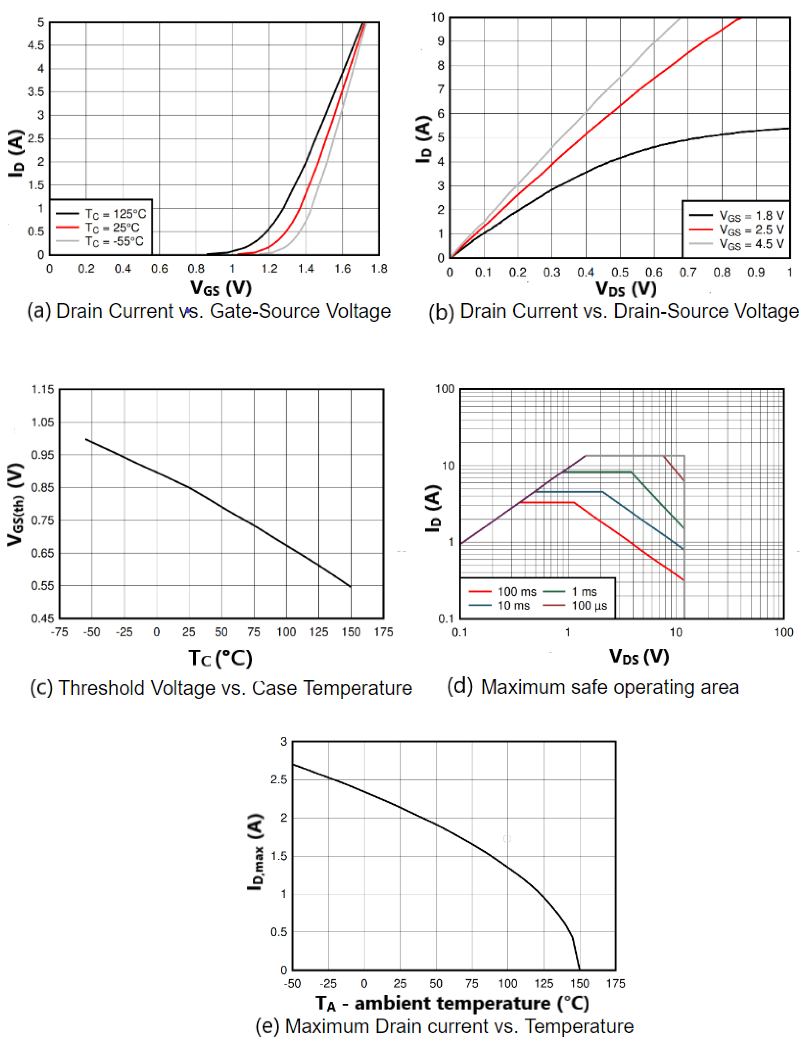
  • Maximum drain-source voltage VDS,max: 12 V
  • Maximum gate-source voltage VGS,max: 8 V
  • Maximum continuous-drain current ID,max: 3.6 A
  • Maximum pulsed-drain current: IDM,max: 13.5 A (pulse duration lower than 100 µs and duty cycle lower than 1%)
  • Operating junction temperature TJ: −55 °C to 150 °C [21].
Figure 5 shows some important characteristics of the CSD13380F3 MOSFET, such as:
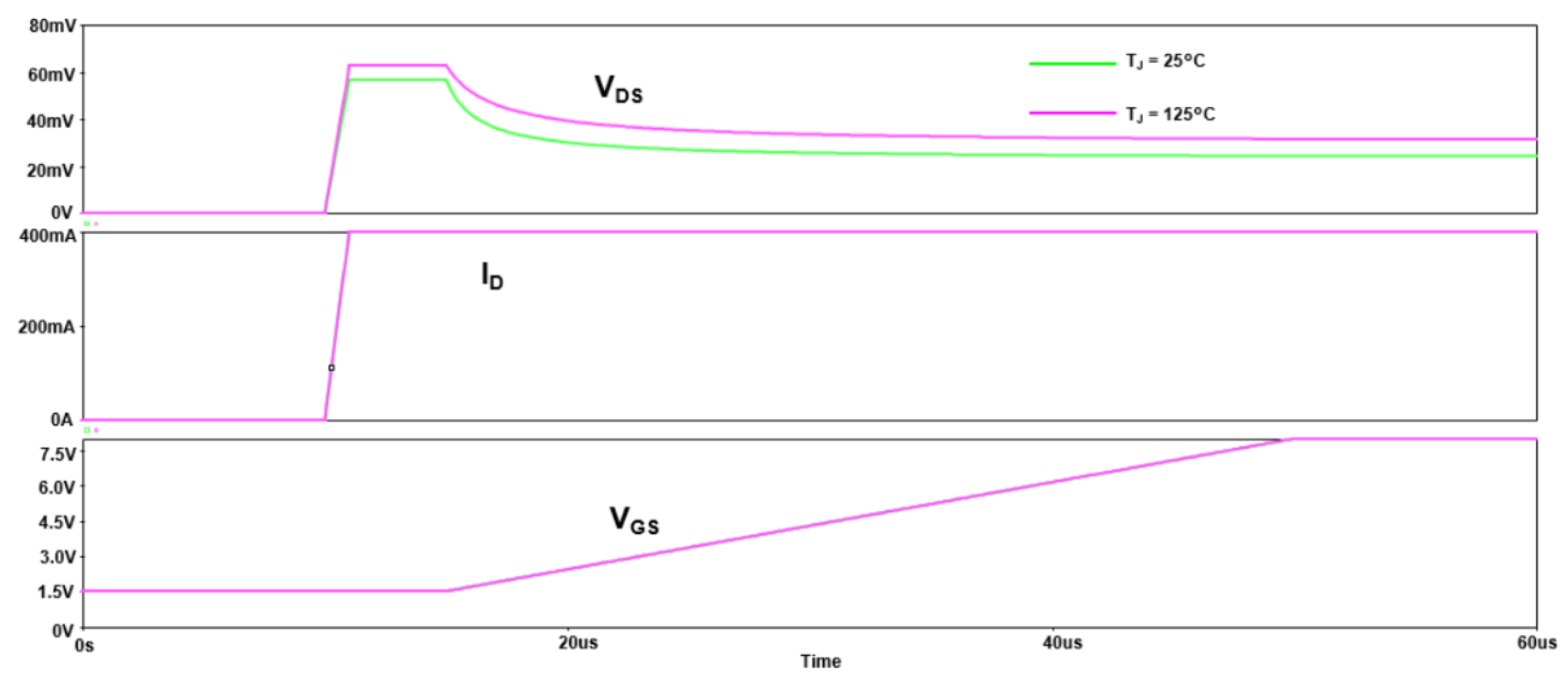
  • Drain Current vs. Gate-Source voltage at three distinct temperatures (−55 °C, 25 °C, 125 °C), where the drain current increases quadratically with VGS after the threshold voltage. This happens due to the drain current iD quadratic dependency on the gate-source voltage vGS when operating in saturation and is detailed in Section 4.
  • Drain Current vs. Drain-Source Voltage at three different VGS voltages (1.8 V, 2.5 V, 4.5 V), where the drain current increases linearly with the drain-source voltage until it saturates. This happens due to the resistor-like behavior of the MOSFET in the linear region. In the saturation region, the drain-source voltage vDS has minimal influence on the drain current iD. More details can be found in Section 4.
  • Threshold Voltage vs. Case Temperature, where the threshold voltage decreases linearly with the increase in temperature, due to the direct dependency of the threshold voltage VT on the thermal voltage k·T/q, where k is the Boltzmann constant (1.380649 × 10⁻²³ m2 kg s−2 K−1) and q is the charge of an electron (1.60217663 × 10⁻¹⁹ C).
  • Maximum safe operating area, which shows that starting with a certain VDS, the maximum drain current decreases. This happens due to the maximum power capabilities of the MOSFET, where the current decreases to limit the power dissipation.
  • Maximum Drain current vs. Temperature curve, which shows that the temperature negatively affects the maximum current. This happens due to the maximum power dissipation allowed on the MOSFET, beyond which the transistor would be destroyed. This characteristic is obtained by experimental results in the laboratory.
The ON-state resistance RDSON vs. Gate-Source voltage VGS characteristic of the CSD13380F3 transistor is presented in Figure 6. The characteristic was determined for a drain current ID = 0.4 A. It can be noticed that at low VGS voltage, RDSON has a higher value (200 mΩ) and decreases based on a square-root dependency until it reaches lower values (79 mΩ at 25 °C and 60 mΩ at 125 °C) at high VGS values (>8 V). RDSON decreases with the VGS increase because the drain current increases, but it saturates at high VGS voltages due to approaching the saturation region conditions. This dependency is mathematically explained in more detail by relations (3)–(7) in Section 4.
The normalized ON-state resistance RDSON vs. Case Temperature characteristic is shown in Figure 7, for two VGS voltages (1.8 V and 4.5 V) and a drain current ID of 0.4 A. In this case, the values are normalized to a temperature of 25 °C (value at a temperature of 25 °C is 1). It can be observed that the MOSFET RDSON increases with the case temperature. The dependency is determined experimentally based on laboratory measurements. The RDSON variation with the temperature is important because the load switches can be used in all types of environments (from cold to hot, as recommended in the manufacturer’s datasheet presented in Figure 7) and they also heat up to high temperatures during functioning at high switching currents.
The starting point in building the new CSD13380F3 MOSFET model using the novel ON-state resistance modeling technique was the simulation of the transistor model provided by Texas Instruments. The model can be downloaded from Texas Instruments’ website [22] and it contains the CSD13380F3 symbol for Orcad Capture (with the extension .olb) and the library file for PSpice Allegro simulator (having the extension .lib). Based on these two files, the simulation test-bench was built and it is used to determine the initial RDSON characteristics presented previously in Figure 6 and Figure 7. The simulation test-bench is displayed in Figure 8, which consists of the piecewise linear voltage source VGS, which sets the gate-source voltage of the MOSFET, the CSD13380F3 MOSFET symbol, and the piecewise linear current source ID that sets the drain current of the transistor.
In the first setup, the gate-source voltage VGS is varied between 1.5 V and 8 V, while the drain current ID is set at 0.4 A. Two simulations are performed corresponding to two junction temperatures TJ (25 °C and 125 °C). The results are presented in Figure 9. It can be seen that the drain-source VDS is influenced by the junction temperature TJ.
The results presented in Figure 9 can be numerically found in Table 1. At a case temperature of 25 °C, the RDSON varies between 141.75 mΩ and 60.92 mΩ, while at 125 °C, RDSON varies between 157.65 mΩ and 78.98 mΩ.
Figure 10 presents the simulated RDSON vs. VGS characteristics for Texas Instruments’ CSD13380F3 model, based on the results obtained in Table 1. It can be noted that at VGS voltages above 2 V, the characteristic is very similar to the theoretical one presented in Figure 6, but at voltages below 2 V, the simulated characteristic does not match the theoretical one. The simulated RDSON for a VGS of 1.5 V is 141.75 mΩ at 25 °C and 157.65 mΩ at 125 °C. The theoretical characteristic is 200 mΩ at VGS = 1.5 V for both temperatures, hence, the relative errors are 29.12% at 25 °C and, respectively, 21.17% at 125 °C, so the simulated RDSON vs. VGS characteristics is not accurate at low VGS voltages The simulation results show that Texas Instruments’ model exhibits large errors for low VGS values.
In order to obtain the normalized RDSON vs. Temperature characteristic presented in Figure 7, the same simulation test-bench as shown in Figure 8 is used. The drain current source ID is set to 0.4 A, as in the previous case. The simulator temperature is swept between −50 °C and 150 °C with a step of 25 °C, while the voltage source VGS varies between 1.8 V and 4.5 V. In order to normalize the characteristic, the initial resulting curves are divided into the 25 °C values for each VGS voltage. Figure 11 presents the second simulation setup used for determining the normalized RDSON vs. Case temperature TC characteristics. Only three temperatures were chosen to be shown in these waveforms (−50 °C, 25 °C, 150 °C) such that the figure is more visible. The downside of the Texas Instrument implementation is that the temperature can only be set as a simulator parameter and cannot be adjusted dynamically during the simulation; hence, the self-heating effect cannot be seen.
The waveforms in Figure 11 are transposed in Table 2, which presents the simulation results along with the calculated RDSON and normalized RDSON for both VGS voltages (1.8 V and 4.5 V) for temperatures between −50 °C and 150 °C. It can be noted that for VGS = 1.8 V, the normalized RDSON varies between 0.83 and 1.34, while for VGS = 4.5 V, the normalized RDSON takes values between 0.83 and 1.4. The temperature step is chosen at 25 °C.
Figure 12 presents the normalized RDSON vs. Case Temperature characteristics for Texas Instruments’ CSD13380F3 MOSFET model, drawn based on results shown in Table 2. It can be seen that until 50 °C, the two curves for VGS = 1.8 V and VGS = 4.5 C are identical and only separate at temperatures above 50 °C. Looking at the theoretical characteristic presented in Figure 7, the two curves are different in each temperature point, except at 25 °C (due to normalization of the results to the 25 °C temperature). The relative errors for the temperature of −50 °C are 2.4% at 1.8 V and 2.3% at 4.5 V, while for the temperature of 150 °C, the relative errors are 2.29% at 1.8 V and 0.7% at 4.5 V.

4. Materials and Methods for the New CSD13380F3 MOSFET Model

As materials, the starting point was the MOSFET functioning equation set. If the gate-source voltage VGS is higher than the threshold voltage VT, the MOSFET can operate either in the linear region or in the saturation region.
The condition needed for the operation in the linear region is VDS < VGS − VT, and the drain current ID can be expressed as [23,24]:
I D = k n ·   W L   · ( V G S V T V D S 2 ) · V D S ,
where kn is transconductance coefficient (A/V2), W is the MOSFET width, L is the MOSFET length, and VDS is the drain-source voltage [7].
For the operation in the saturation region, the condition is VDS ≥ VGS − VT, and the drain current ID becomes independent of the VDS voltage if the channel length modulation effect is neglected [23,24]:
I D = k n 2   ·   W L   · ( V G S V T ) 2
The novel ON-state resistance modeling principle is shown in Figure 13. The first step in the implementation of the above equations into the new model consists of setting the target ON-state resistance RDSON,t chosen by the user based on the catalogue data, which can be a function of temperature, VGS, and load current, depending on the information that the user has. Next step is the calculation of the theoretical drain gate-source voltage VGS,t based on the specified RDSON,t and the monitored drain current ID. When VGS,t is applied as the gate-source voltage, the transistor ON-state resistance automatically sets at RDSON,t.
Based on (1), the transistor’s VDS for the transistor operating at RDSON,t becomes:
V D S = R D S O N , t · I D
By replacing (5) in (3), the drain current ID becomes:
I D = k n · W L · [ ( V G S V T ) · R D S O N , t · I D R D S O N , t 2 · I D 2 2   ]
The theoretical gate-source voltage VGS,t, which assures that the transistor ON-state resistance is RDSON,t is calculated based on (6) as follows:
V G S , t = 1 V + 2 + k n · W L · I D · R D S O N , t 2 2 · k n · W L · R D S O N , t
The transistor model senses the VGS voltage that is set externally and based on its value, along with the temperature and drain current ID, chooses the appropriate theoretical RDSON,t value. Based on the drain current ID and the RDSON,t value, the actual VGS controlling the transistor is set to VGS,t.
The PSpice CSD13380F3 model source code is presented in Figure 14. The voltage sources EA1, EA2, and EA3 are used to define the normalizing factor. Based on the normalizing factor, the target RDSON,t is set. The drain current ID is monitored through 0 V voltage source VSENSE. The RDSON,t and monitored ID are then used to define the target gate-source voltage VGS,t. A generic NMOS transistor is also used. Its parameters are not important, since the gate-source voltage automatically adapts in order to set the correct RDSON value.

5. Simulation Results for the New CSD13380F3 MOSFET Model

The OrCAD Capture simulation test-bench of the new CSD13380F3 MOSFET model is presented in Figure 15. Additionally, from the test-bench shown in Figure 8, there is a fourth pin, TJ, which is the device temperature as a voltage. The advantage of this implementation is that the temperature can vary during the simulation and emulate the self-heating effect, which plays an important role in load switches. The same steps as for the Texas Instruments’ model are applied. For the RDSON vs. VGS characteristic, the current source is set to 0.4 A and the VGS voltage source is swept between 1.5 V and 8 V.
The setup used to determine the new RDSON vs. VGS characteristics is shown in Figure 16. The drain current is set to 0.4 A and VGS varies between 1.5 V and 8 V for two junction temperatures (25 °C and 125 °C). It can be seen that the junction temperatures influence the VDS voltage.
The waveforms shown in Figure 16 are also linked to Table 3, which presents the RDSON calculations for the new CSD13380F3 model at VGS between 1.5 V and 8 V for temperatures of 25 °C and 125 °C. It can be seen that at 25 °C, RDSON varies between 200 mΩ and 60 mΩ, while at 125 °C, RDSON varies between 200 mΩ and 78.6 mΩ, just like in the theoretical characteristic shown in Figure 6.
Figure 17 presents the simulated RDSON vs. VGS characteristic for the newly implemented CSD13380F3 model, based on the measurements in Table 3. It can be seen that the RDSON vs. VGS characteristic of the newly implemented model matches the theoretical one shown in Figure 6, and the relative error in all voltage points is 0 or very close to 0. These remarkable obtained results prove the very high accuracy of the proposed modeling method.
The same simulation test-bench presented in Figure 15 is used to determine the normalized RDSON vs. Temperature characteristics of the newly implemented model. For this setup, the drain current is set to 0.4 A and the temperature TJ is varied between −50 °C and 150 °C. Two simulations are performed for VGS = 1.8 V and VGS = 4.5 V. The waveforms are presented in Figure 18. It can be noted that the VDS voltage is influenced by VGS and TJ.
The waveforms in Figure 18 are also used to create Table 4, which contains the simulation results of the new CSD13380F3 model along with the calculated RDSON and normalized RDSON for both VGS voltages (1.8 V and 4.5 V) V for temperatures between −50 °C and 150 °C, with a chosen step of 25 °C. It can be noted that for VGS = 1.8 V, the normalized RDSON varies between 0.85 and 1.31, as stated before, while for VGS = 4.5 V, the normalized RDSON takes values between 0.82 and 1.41.
Figure 19 presents the normalized RDSON vs. Case Temperature characteristic for the new CSD13380F3 MOSFET model, based on the results obtained in Table 4. It can be seen that the characteristic matches the theoretical one in Figure 7, the values in each frequency point being identical, which proves the value of the newly implemented model.

6. Discussion and Comparison of Theoretical, Old, and New ON-State Resistance Characteristics Implementations

Table 5 compares the theoretical RDSON vs VGS characteristics of the CSD13380F3 transistor with the old Texas Instruments’ and the new proposed implementations. The relative error to the theoretical characteristic of the Texas Instruments’ model (RSDON,TI Error) varies between 0.08% and 29.12%, while for the new model, the relative error (RDSON,new Error) varies between 0% and 0.08%, which proves the enhancement of the new model compared to the model designed by Texas Instruments.
Table 6 compares the theoretical normalized RDSON vs Case temperature characteristics of the CSD13380F3 transistor with the ones obtained with the old Texas Instruments’ model and the new proposed MOSFET model. For the Texas Instruments’ model, the normalized RDSON,TI relative error varies between 0% and 2.35%, while for the new model, the normalized RDSON,new relative error varies between 0% and 0.8%, which proves once again the performance of the new proposed model.
The Texas Instruments’ implementation uses a generic NMOS transistor in which the parameters are set to certain values. This way, it is impossible to control the RDSON precisely over a wide domain of temperatures and voltages. The advantage of this novel technique is that, in addition to using a generic NMOS transistor, it monitors the temperature, load current, and automatically adapts internally the applied VGS voltage, such that the transistor RDSON matches the theoretical value. Hence, the RDSON accuracy can be kept over the entire range of temperatures, currents, or voltages.

7. Conclusions

In this paper, for the first time, a novel ON-state resistance modeling technique for MOSFET power switches was presented, which is based on modulating the gate-source voltage of the MOSFET such that the target RDSON is obtained.
The new proposed method combines mathematical relations and circuits’ relations, as follows:
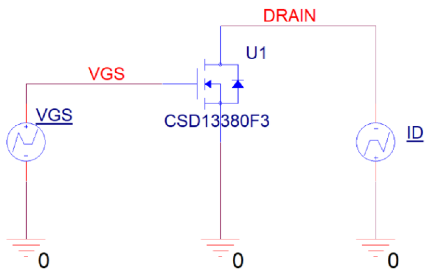
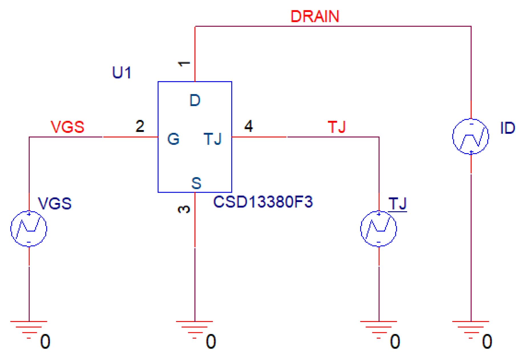
  • The starting point was a transistor model existing on the market, CSD13380F3, from Texas Instruments, which is a 12 V N-channel MOSFET that can be used for load switching applications. The transistor’s model is available on the website of Texas Instruments [22] and contains the transistor symbol and the PSpice library file.
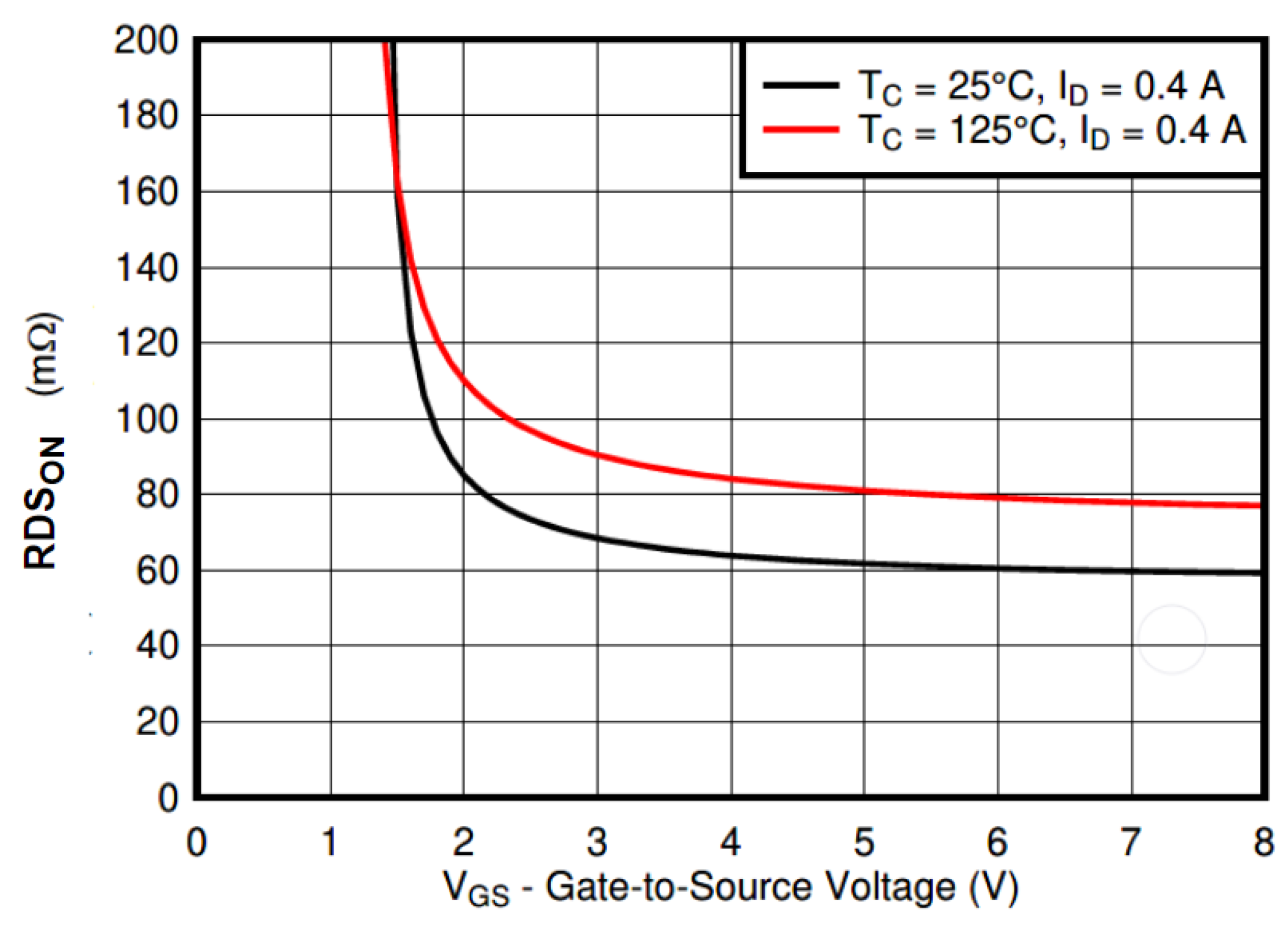
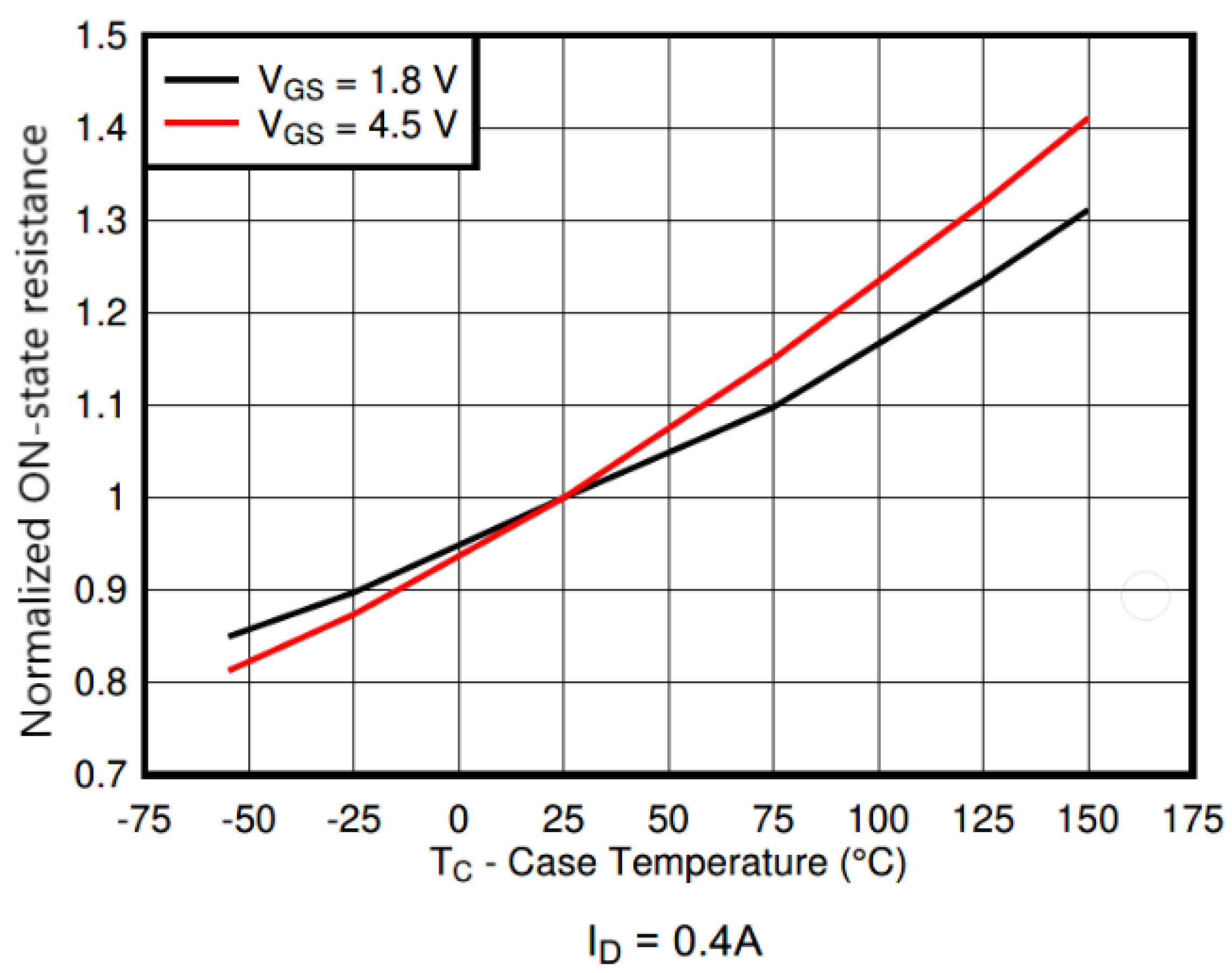
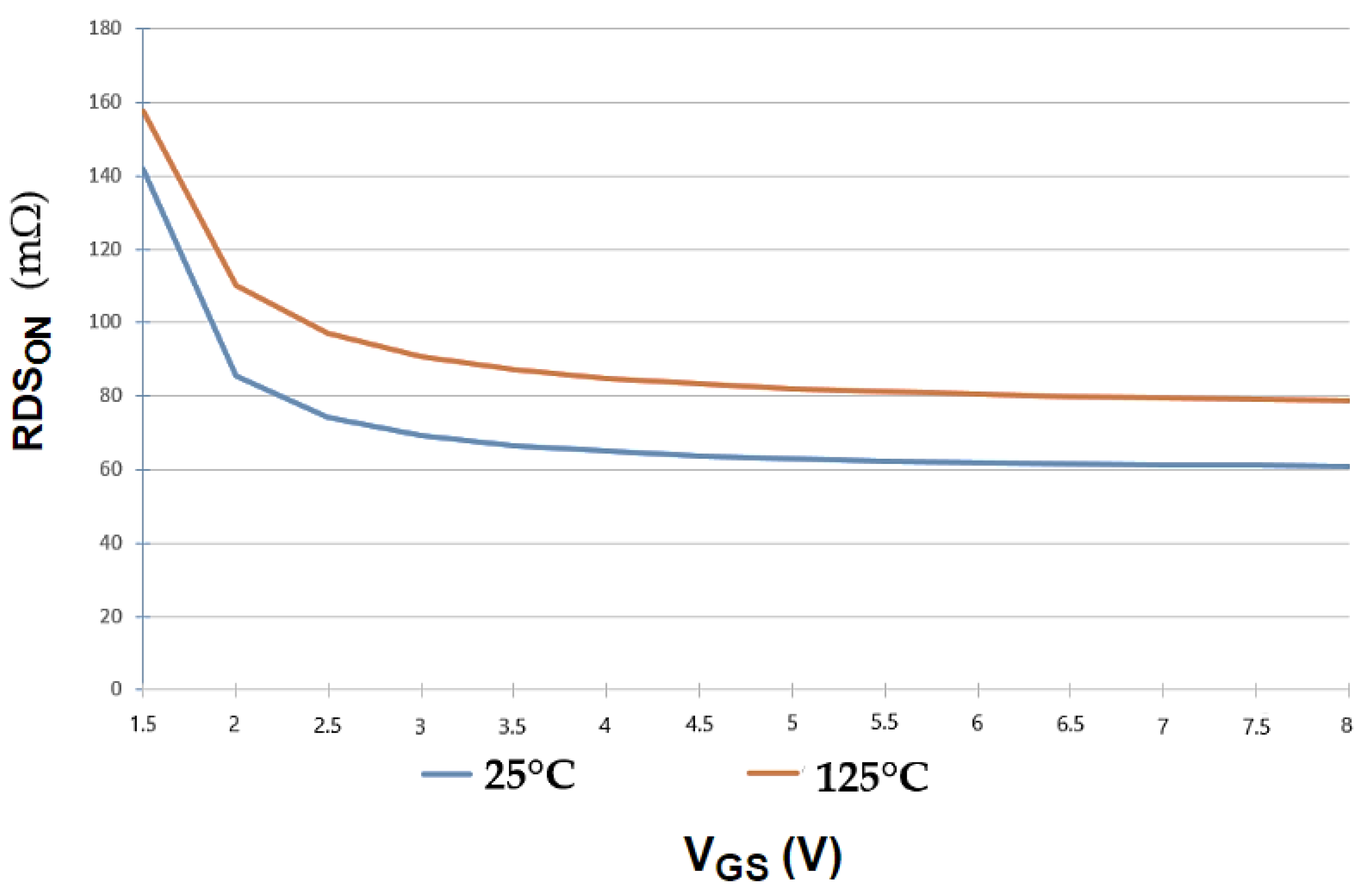
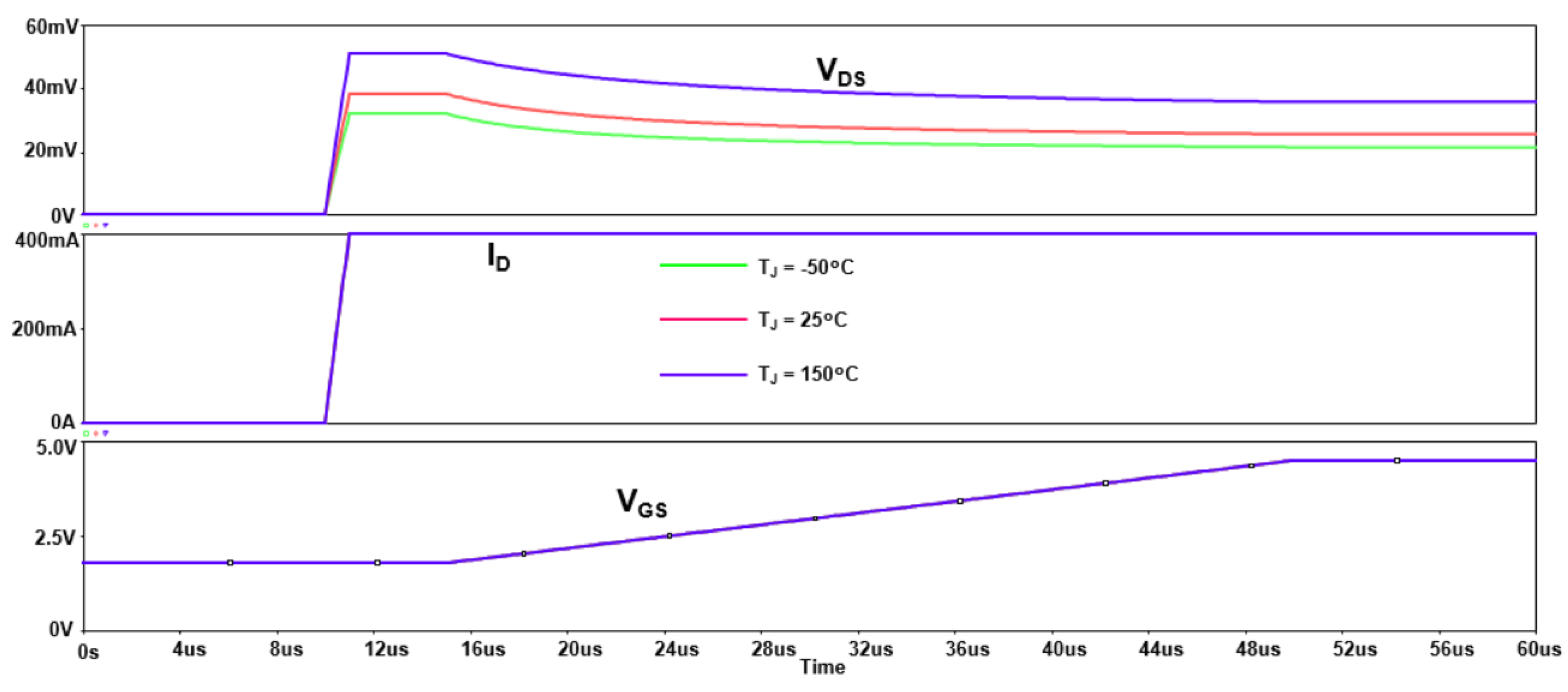
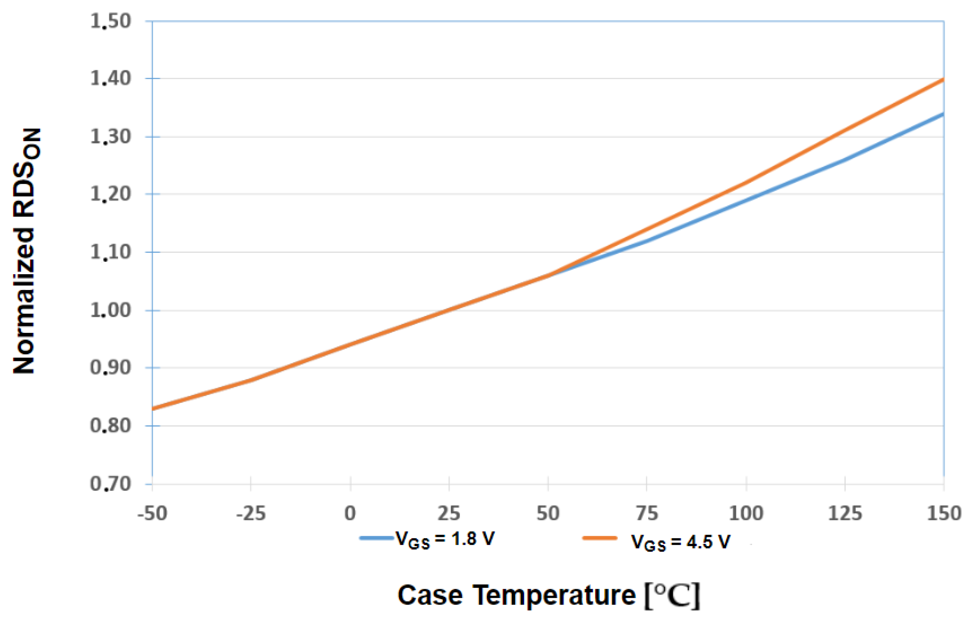
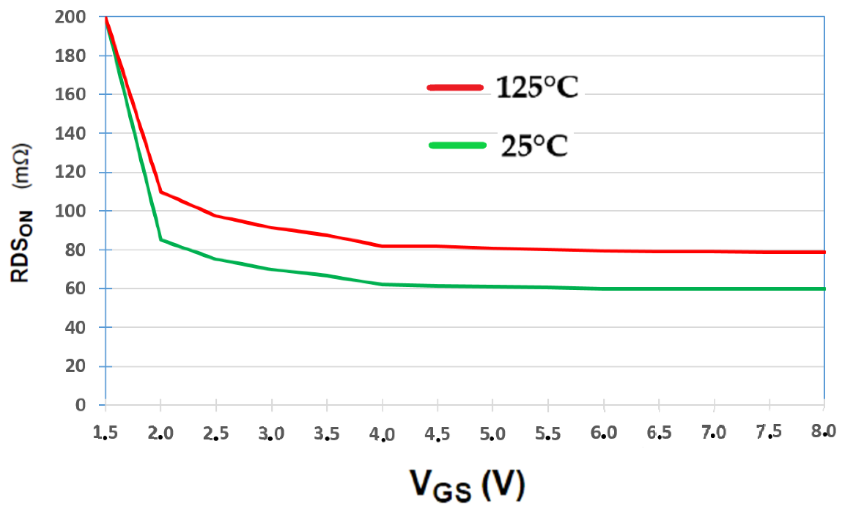
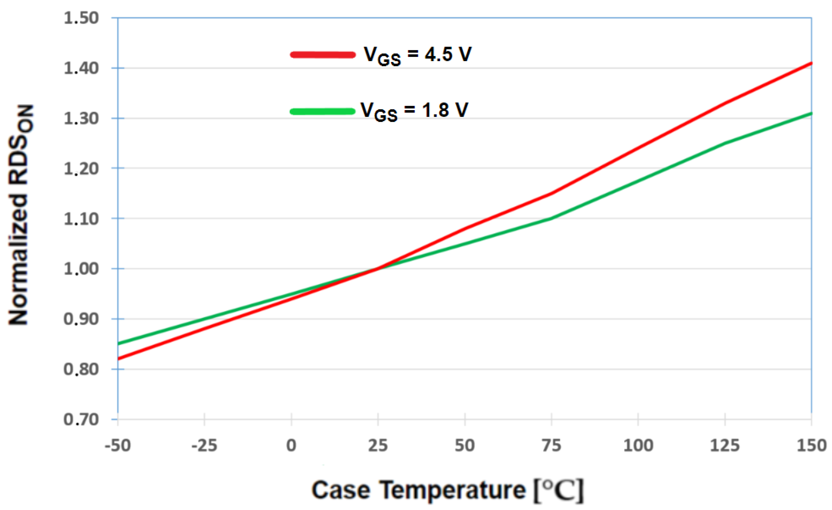
  • Firstly, the transistor model designed by Texas Instruments was simulated using OrCAD Capture environment and its RDSON vs. VGS characteristics at 25 °C and 150 °C, along with the RDSON vs. Case Temperature at VGS = 1.8 V and VGS = 4.5 V were plotted. The RDSON vs. VGS relative error to the theoretical characteristics varies between 0.08% and 29.12%, while the RDSON vs. Case Temperature error varies between 0% and 2.35%. It was noticed that the temperature can be set only as a simulator parameter and cannot be modified dynamically during the simulation.
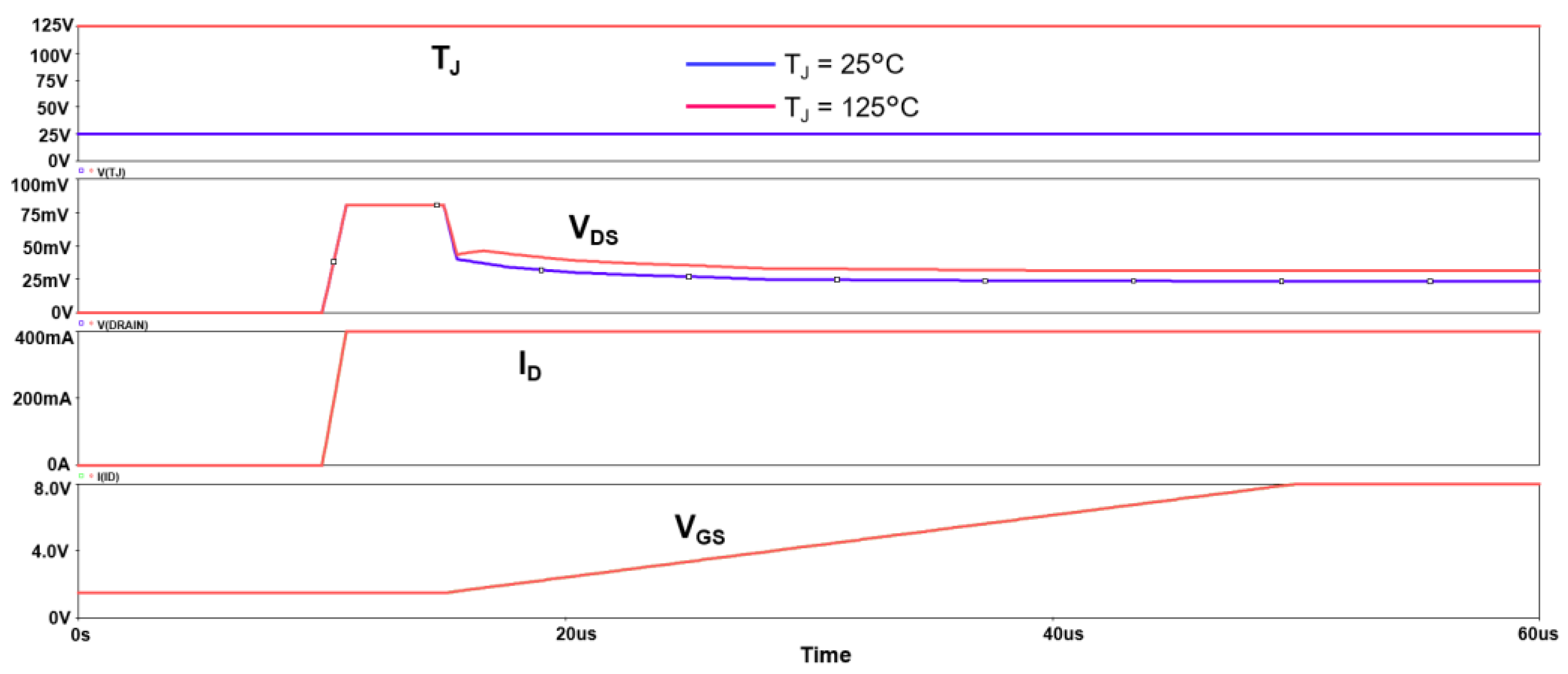
  • Afterwards, the new CSD13380F3 MOSFET model was implemented using the novel RDSON modeling technique. This technique calculates the necessary voltage VGS needed, such that the MOSFET switch operates at a certain RDSON. When setting the VGS externally, the RDSON value automatically sets at the target value and the only input needed from the user is the theoretical RDSON characteristic.
  • After simulating the newly proposed model, the RDSON vs. VGS and RDSON vs. Case Temperature characteristics were plotted. The relative error for the RDSON vs. VGS curves varies between 0% and 0.08%, while the relative error for the RDSON vs. Case Temperature characteristics is between 0% and 0.8%.
Comparing the Texas Instruments’ model and the newly implemented model, the advantages are:
The new model accurately matches the datasheet characteristics presented in Figure 6 and Figure 7. The maximum error obtained for this new model is 0.8%, whereas the maximum Texas Instruments model error is 29.12%.
The new MOSFET model has an independent temperature pin, which allows the user to adjust the temperature dynamically during the simulation and, in this way, can emulate the self-heating effect of the transistor.
The novel ON-state resistance modeling technique allows for the accurate modeling of any MOSFET power switch only by defining the datasheet RDSON variation. The literature does not provide any research on modeling the RDSON in all possible corners, only at discrete temperature and/or voltages, so the new proposed method is a breakthrough in the simulation domain and can be used successfully in creating accurate MOSFET behavioral models.
A transistor model created using the novel RDSON modeling technique is able to match the real behavior of the component over the entire operating range, thus, assuring compatibility between simulation and physical testing.
Highly reliable MOSFET power switch models can be built using the new technique in a fast and efficient manner, only by defining the theoretical RDSON characteristics.
The implementation achieved in this paper also proves extremely important in the electronics domain, where the simulation has become the main testing concept. Through simulation, the engineers are able to validate the circuit before the physical implementation and this avoids additional costs involved by faults present in the circuit’s design. Since the MOSFET transistors are found in many applications (low-dropout linear voltage regulators, switching regulators, gate drivers, battery management systems), it is mandatory to create accurate behavioral models for them, but in order to achieve this goal, an essential parameter must be taken into consideration, namely the ON-state resistance. Using the novel technique presented in this paper, the transistor model RDSON accuracy can be kept over the entire range of temperatures, currents, or voltages.
Other future research directions consist of enhancements in the current CSD13380F3 MOSFET model in order to integrate the output voltage slew rate setting when using the transistor as a MOSFET switch.

Author Contributions

Conceptualization, I.-C.G., A.F. and L.A.P.; methodology, I.-C.G., A.F. and L.A.P.; software, I.-C.G.; validation, I.-C.G., A.F. and L.A.P.; formal analysis, I.-C.G., A.F. and L.A.P.; investigation, I.-C.G.; resources, I.-C.G., A.F. and L.A.P.; data curation, I.-C.G., A.F. and L.A.P.; writing—original draft preparation, I.-C.G.; writing—review and editing, A.F. and L.A.P.; visualization, A.F. and L.A.P.; supervision, A.F. and L.A.P.; project administration, I.-C.G., A.F. and L.A.P.; funding acquisition, A.F. and L.A.P. All authors have read and agreed to the published version of the manuscript.

Funding

This work was supported by a grant from the Romanian Ministry of Education and Research, CCCDI—UEFISCDI, project number PN-III-P2-2.1-PED-2019-2862, within PNCDI III.

Data Availability Statement

Data is contained within the article.

Conflicts of Interest

The authors declare no conflict of interest.

References

  1. Pratap, R.; Singh, R.K.; Agarwal, V. SPICE Model development for SiC Power MOSFET. In Proceedings of the 2012 IEEE International Conference on Power Electronics, Drives and Energy Systems(PEDES), Bengaluru, India, 16–19 December 2012; pp. 1–5. [Google Scholar]
  2. Baba, S.; Gieraltowski, A.; Jasinski, M.; Blaabjerg, F.; Bahman, A.; Zelechowski, M. Active Power Cycling Test Bench for SiC Power MOSFETs—Principles, Design, and Implementation. IEEE Trans. Power Electronics 2021, 36, 2661–2675. [Google Scholar] [CrossRef]
  3. Galadi, A. Dynamic model of power Mosfet for Spice circuit simulation. In Proceedings of the 2019 IEEE 5th International Conference on Optimization and Applications (ICOA), Kenitra, Morocco, 25–26 April 2019; pp. 1–4. [Google Scholar]
  4. Bayant Jaliga, B. Advanced Power Mosfet Concepts; Springer: New York, NY, USA, 2010; pp. 1–4. [Google Scholar]
  5. Barkhordarian, V. Power Mosfet Basics. Available online: https://www.infineon.com/dgdl/mosfet.pdf?fileId=5546d462533600a4015357444e913f4f (accessed on 8 September 2022).
  6. Zhao, W.; Wei, P. PSpice system simulation application in electronic circuit design. In Proceedings of the 32nd Chinese Control Conference, Xi’an, China, 26–28 July 2013; pp. 8634–8636. [Google Scholar]
  7. Cadence Design System. In PSpice Reference Guide, 2nd ed.; Cadence Design Systems: Tigard, OR, USA, 2000.
  8. Berry, A.; Brown, A.; Clifton, B.; Dyer, J. The Power MOSFET Application Handbook; Design Engineer’s Guide; NXP Semiconductors: Manchester, UK, 2017; pp. 19–30. [Google Scholar]
  9. Stefanskyi, A.; Starzak, L.; Napieralski, A.; Lobur, M. Analysis of SPICE models for SiC MOSFET power devices. In Proceedings of the 2017 IEEE 14th International Conference The Experience of Designing and Application of CAD Systems in Microelectronics (CADSM), Lviv, Ukraine, 21–25 February 2017; pp. 79–81. [Google Scholar]
  10. He, C.; Victory, J.; Xiao, Y.; Vleeschouwer, H.; Zheng, E.; Hu, Z. SiC MOSFET Corner and Statistical SPICE Model Generation. In Proceedings of the 2020 IEEE 32nd International Symposium on Power Semiconductor Devices and ICs (ISPSD), Vienna, Austria, 13–18 September 2020. [Google Scholar]
  11. Hsu, F.-J.; Yen, C.-T.; Hung, C.-C.; Lee, C.-Y.; Lee, L.-S.; Chu, K.-T.; Li, Y.-F. High accuracy large-signal SPICE model for silicon carbide MOSFET. In Proceedings of the 2018 IEEE 30th International Symposium on Power Semiconductor Devices and ICs (ISPSD), Chicago, IL, USA, 13–14 May 2018; pp. 403–406. [Google Scholar]
  12. Borghese, A.; Riccio, M.; Maresca, L.; Breglio, G.; Irace, A. An Electrothermal Compact Model for SiC MOSFETs Based on SPICE Primitives with Improved Description of the JFET Resistance. In Proceedings of the 2022 IEEE 34th International Symposium on Power Semiconductor Devices and ICs (ISPSD), Vancouver, BC, Canada, 22–25 May 2022; pp. 37–40. [Google Scholar]
  13. Batarseh, I.; Harb, A. Power Electronics. Circuit Analysis and Design, 2nd ed.; Springer: Cham, Switzerland, 2018; pp. 60–67. [Google Scholar]
  14. Lu, B.; Cui, M.; Liu, W. The Impact of AlGaN Barrier on Transient VTH Shifts and VTH Hysteresis in Depletion and Enhancement mode AlGaN/GaN MIS-HEMTs. In Proceedings of the 2019 IEEE International Conference on IC Design and Technology (ICICDT), Suzhou, China, 17–19 June 2019; pp. 1–4. [Google Scholar]
  15. Zhang, B.; Wang, J.; Wang, C.; Wang, X.; Huang, C.; He, J.; Wang, M.; Mo, J.; Hu, Y.; Wu, W. Monolithic Integration of GaN-Based Enhancement/Depletion-Mode MIS-HEMTs With AlN/SiN Bilayer Dielectric. IEEE Electron Device Lett. 2022, 43, 1025–1028. [Google Scholar] [CrossRef]
  16. Marshall Leach, W. The MOSFET; Georgia Institute of Technology, School of Electrical and Computer Engineering: Atlanta, Georgia, 2010; pp. 1–10. [Google Scholar]
  17. Liou, J.J.; Ortiz-Conde, A.; Garcia-Sanchez, F. Analysis and Design of MOSFETs. Modeling, Simulation and Parameter Extraction; Springer Science + Business Media: New York, NY, USA, 1998; pp. 216–220. [Google Scholar]
  18. Load Switches. Available online: https://www.nxp.com/products/power-management/load-switches:MC_71730 (accessed on 13 September 2022).
  19. High-Side Switches and MOSFET Drivers. Available online: https://www.analog.com/en/parametricsearch/11395#/ (accessed on 13 September 2022).
  20. N-channel MOSFETs. Available online: https://www.ti.com/power-management/mosfets/n-channel-transistors/overview.html (accessed on 13 September 2022).
  21. CSD13380F3 12-V N-Channel FemtoFET MOSFET. 2022. Available online: https://www.ti.com/lit/ds/sylink/csd13380f3.pdf?ts=1663568836532&ref_url=https%253A%252F%252Fwww.google.com%252F (accessed on 19 September 2022).
  22. Texas Instruments. Available online: www.ti.com (accessed on 20 September 2022).
  23. Cheung, N. MOSFET I-V Analysis. EE143 Lecture #24; University of California: Berkeley, CA, USA.
  24. Palermo, S. Analog & Mixed-Signal Center, ECEN474: (Analog) VLSI Circuit Design Fall 2012. Lecture 4: MOS Transistor Modeling; Texas A&M University: College Station, TX, USA, 2012. [Google Scholar]
Figure 1. Power device categories [4].
Mathematics 11 00072 g001
Figure 2. MOSFET transistor symbols [16].
Mathematics 11 00072 g002
Figure 3. Ideal MOSFET power switch characteristics [4,13].
Mathematics 11 00072 g003
Figure 4. Real MOSFET power switch characteristics [13].
Mathematics 11 00072 g004
Figure 5. CSD13380F3 MOSFET characteristics [21].
Mathematics 11 00072 g005
Figure 6. RDSON vs. VGS characteristic of CSD13380F3 [21].
Mathematics 11 00072 g006
Figure 7. Normalized ON-state resistance vs. Case temperature [21].
Mathematics 11 00072 g007
Figure 8. Simulation test-bench for CSD13380F3.
Mathematics 11 00072 g008
Figure 9. Simulation setup for determining the Texas Instruments CSD13380F3 model RDSON vs. VGS characteristics.
Mathematics 11 00072 g009
Figure 10. Simulated RDSON vs. VGS for Texas Instruments’ CSD13380F3 model.
Mathematics 11 00072 g010
Figure 11. Simulation setup for determining the Texas Instruments CSD13380F3 model normalized RDSON vs. TC characteristics.
Mathematics 11 00072 g011
Figure 12. Simulated RDSON vs. Case Temperature for Texas Instruments’ CSD13380F3 model.
Mathematics 11 00072 g012
Figure 13. Novel ON-state resistance modeling principle.
Mathematics 11 00072 g013
Figure 14. PSpice CSD13380F3 model source code.
Mathematics 11 00072 g014
Figure 15. Simulation test-bench for the new CSD13380F3 model.
Mathematics 11 00072 g015
Figure 16. Simulation setup for determining the new CSD13380F3 model RDSON vs. VGS characteristics.
Mathematics 11 00072 g016
Figure 17. Simulated RDSON vs. VGS for the new CSD13380F3 model.
Mathematics 11 00072 g017
Figure 18. Simulation setup for determining the Texas new CSD13380F3 model normalized RDSON vs. TC characteristics.
Mathematics 11 00072 g018
Figure 19. Simulated RDSON vs. Case Temperature for Texas the new CSD13380F3 model.
Mathematics 11 00072 g019
Table 1. RDSON vs. VGS calculations for Texas Instruments’ model.
TCASE = 25 °C
IDVGSVDSRDSON
[A][V][mV][mΩ]
0.41.556.7141.75
0.4234.2585.62
0.42.529.7274.3
0.4327.7569.39
0.43.526.6766.68
0.442664.98
0.44.525.5363.82
0.4525.263
0.45.524.9562.39
0.4624.7761.93
0.46.524.6361.58
0.4724.5261.3
0.47.524.4361.09
0.4824.3760.92
TCASE = 125 °C
0.41.563.06157.65
0.4244.11110.29
0.42.538.8897.2
0.4336.3890.96
0.43.534.9387.33
0.443484.97
0.44.533.3383.34
0.4532.8682.15
0.45.532.581.26
0.4632.2280.57
0.46.53280.03
0.4731.8479.6
0.47.531.779.26
0.4831.5978.98
Table 2. RDSON vs. Temperature simulation results for Texas Instruments’ model.
VGS = 1.8 V
IDTCASEVDSRDSONNormalized RDSON
[A][°C][mV][mΩ]
0.4−5031.8179.530.83
0.4−2533.7984.490.88
0.4035.8989.740.94
0.42538.1195.291
0.45040.46101.161.06
0.47542.94107.361.12
0.410045.55113.881.19
0.412548.29120.731.26
0.415051.16127.911.34
VGS = 4.5 V
0.4−5021.1952.970.83
0.4−2522.4256.060.88
0.4023.8259.560.94
0.42525.3963.491
0.45027.1367.831.06
0.47529.0372.591.14
0.410031.177.761.22
0.412533.3383.341.31
0.415035.7389.331.4
Table 3. RDSON vs. VGS calculations for the new CSD13380F3 model.
TCASE = 25 °C
IDVGSVDSRDSON
[A][V][mV][mΩ]
0.41.580200
0.423485
0.42.53075
0.432870
0.43.526.666.5
0.4424.862
0.44.524.661.5
0.4524.461
0.45.524.260.5
0.462460
0.46.52460
0.472460
0.47.52460
0.482460
TCASE = 125 °C
0.41.580200
0.4243.86109.65
0.42.538.9497.35
0.4336.5691.41
0.43.534.9587.38
0.4432.7881.96
0.44.532.7181.8
0.4532.3880.95
0.45.532.0480.12
0.4631.7179.3
0.46.531.6479.11
0.4731.5778.94
0.47.531.578.77
0.4831.4478.6
Table 4. RDSON vs. Temperature simulation results for the new CSD13380F3 model.
VGS = 1.8 V
IDTCASEVDSRDSONNormalized RDSON
[A][°C][mV][mΩ]
0.4−5031.4578.620.85
0.4−2533.383.250.9
0.4035.1587.870.95
0.4253792.51
0.45038.8597.121.05
0.47540.7101.751.1
0.410043.47108.681.175
0.412546.25115.621.25
0.415048.47121.171.31
VGS = 4.5 V
0.4−5020.1750.430.82
0.4−2521.6454.120.88
0.4023.1257.80.94
0.42524.661.51
0.45026.5666.421.08
0.47528.2970.721.15
0.410030.576.251.24
0.412532.7181.81.33
0.415034.6886.711.41
Table 5. RDSON vs. VGS characteristics comparison.
TCASE = 25 °C
VGSRDSON,theoreticalRDSON,TIRDSON,TI ErrorRDSON,newRDSON,new Error
[V][mΩ][mΩ][%][mΩ][%]
1.5200141.7529.122000
28585.620.72850
2.57574.30.93750
37069.390.87700
3.566.566.680.2766.50
46264.984.8620
4.561.563.823.7761.50
561633.27610
5.560.562.393.1260.50
66061.933.21600
6.56061.582.63600
76061.32.16600
7.56061.091.81600
86060.921.53600
TCASE = 125 °C
1.5200157.6521.172000
2109.6110.290.62109.650.04
2.597.397.20.197.350.05
391.490.960.4891.410.01
3.587.487.330.0887.380.02
48284.973.6281.960.04
4.581.883.341.8881.80
580.982.151.5480.950.06
5.580.181.261.4480.120.02
679.380.571.679.30
6.579.180.031.1779.110.01
77979.60.7578.940.07
7.578.779.260.7178.770.08
878.678.980.4878.60
Table 6. RDSON vs. Case temperature characteristic comparison.
VGS = 1.8 V
TemperatureNormalized RDSON,theoreticalNormalized
RDSON,TI
Normalized
RDSON,TI Error
Normalized
RDSON,new
Normalized
RDSON,new Error
[°C] [%] [%]
−500.850.832.350.850
−250.90.882.220.90
00.950.941.050.950
2511010
501.051.060.951.050
751.11.121.811.10
1001.181.190.841.1750.42
1251.241.261.611.250.8
1501.311.342.291.310
VGS = 4.5 V
−500.820.831.210.820
−250.880.8800.880
00.940.9400.940
2511010
501.081.061.851.080
751.151.140.861.150
1001.241.221.611.240
1251.321.310.751.330.75
1501.411.40.71.410
Disclaimer/Publisher’s Note: The statements, opinions and data contained in all publications are solely those of the individual author(s) and contributor(s) and not of MDPI and/or the editor(s). MDPI and/or the editor(s) disclaim responsibility for any injury to people or property resulting from any ideas, methods, instructions or products referred to in the content.

