1. Introduction
In recent years, the automotive domain has seen an increase in the complexity of modern cars, which will continue to become increasingly complex. The number of electronic functions and components in cars is also rapidly increasing, which can lead to design problems in complex modular systems [
1].
Supplying and conditioning electrical power are the most important features of an electrical system. No application can fully perform its function without a stable supply. Batteries, generators, and other off-line supplies provide substantial voltage and current variations over time and over a wide range of operating conditions [
2]. Noise is produced due to their inherent nature, but also by high-power switching circuits such as DC–DC converters, controllers for electric motors, actuators, and relays. This noise analysis is increasingly important in the case of Electric Vehicles (EVs) or Hybrid Electric Vehicles (HEV) from the Electromagnetic Interference (EMI) point of view [
2,
3].
Rapidly changing loads result in unwanted voltage changes and frequency harmonics over an ideal direct current (DC) component. The goal of a voltage regulator is to convert the noisy supply into a stable, accurate, load-independent voltage and hence attenuate the fluctuations to desired levels [
2,
3,
4]. One of the most used power supply circuits in the automotive domain is the low dropout (LDO) voltage regulator, which uses a unipolar MOS or a bipolar pass transistor in its structure as a series control element to provide a regulated output voltage over a wide range of supply voltages or load current variations [
5,
6,
7,
8].
Simulation is used in the automotive domain for the validation of a design before physical implementation, and can indicate flaws and faults in the design process or reinforce the correct functioning of the system. For a highly reliable simulation, accurate component models are necessary, for which the simulated behavior must be as close as possible (ideally, identical) to the real behavior. Simulation Program for Integrated Circuits Emphasis (SPICE) is a general-purpose analog and mixed-mode simulator that is used to verify and predict circuit behavior. PSpice is the PC version of SPICE, and is used to simulate the behavior of circuits on a digital computer, emulating the signal generators, multimeters, oscilloscopes, and frequency spectrum analyzers, and includes analog and digital libraries of standard components. As a result, it is an important tool for a wide range of analog and digital applications [
9].
In automotive design, internal clean power supplies having a high Power Supply Rejection Ratio (PSRR) are a vital requirement to increase power management efficiency in system-on-chip circuitry [
10].
The literature focuses only on PSRR physical design and measurement [
3,
5,
7,
10], and does not provide any research on PSRR modeling techniques. This paper proposes an optimization approach in the simulation domain, and emphasizes a highly accurate method of modeling the PSRR for automotive LDOs. The main contributions are listed below:
implementation of a new PSRR model for the TPS785-Q1 automotive LDO from Texas Instruments;
simulation of the LDO model with the initial PSRR functionality, as is currently commercially available;
simulation of the LDO model with the new PSRR functionality added using the PSpice Allegro simulator and OrCAD Capture CIS 17.2 simulation environment;
comparison of the results using the values of the theoretical and previous approaches.
The remainder of the paper is organized as it follows:
Section 2 shows the background related to this work and presents the currently existing PSRR vs. frequency characteristic of TPS785-Q1 from Texas Instruments,
Section 3 emphasizes the materials and methods for the new PSRR model implementation, and
Section 4 presents the numerical simulation results in tables and waveform figures. The comparison between the theoretical, previous, and new PSRR characteristics of the TPS785-Q1 model is presented in
Section 5. The conclusions are synthesized in
Section 6.
2. Background of LDO PSRR
The LDO is commonly used in power electronics design as the last stage of the power-distribution tree. In the first stage, an intermediate voltage is obtained from the input voltage of a supply system using other topologies, such as DC–DC or AC–DC converters. These topologies introduce harmonics and supraharmonics, generating a noisy intermediate voltage. The supraharmonics are defined as current and voltage waveforms distortion within the range 2–150 kHz, that can be intentionally created by power line communication systems or unintentionally by power electronic converters. In stage two, the LDO regulator generates the system output voltage from the intermediate voltage. The objective is to achieve a high power conversion efficiency in stage one and to remove the switching noise in stage two. The noise can be technically translated into an unwanted voltage ripple that must be eliminated [
11], thus justifying the study of PSRR in this paper. For example, in automotive applications, the car battery delivers the supply voltage that can vary between 6 and 30 V, having slew rates of up to 1 V/µs. In addition, the load current can vary drastically, with slew rates of up to 50–100 mA/µs. These very high slew-rates also introduce harmonics, which translate into unwanted voltage spikes that must also be eliminated; this elimination is also achieved by the new proposed PSRR model [
6].
The simplified working principle of a regular LDO voltage regulator is shown in
Figure 1, and contains the input voltage
VIN, the pass transistor element Q, the error amplifier K, and the resistive network (R
1, R
2), which sets the desired output voltage
VOUT. The error amplifier compares the positive terminal voltage of
VOUT ∗ [R
2/(R
1 + R
2)] with the reference voltage V
REF connected to the negative terminal and drives the pass transistor accordingly such that the two voltages become equal.
The most common characteristics that need to be taken into consideration when creating a LDO voltage regulator model are: output voltage accuracy, line regulation, load regulation, current consumption, dropout voltage, output voltage slew-rate, protections, and PSRR [
13,
14].
Some examples of these characteristics are presented in
Figure 2a–f, being taken from Texas Instruments’ TPS785-Q1 automotive LDO product [
14].
Existing LDO models are commercially available from companies such as Texas Instruments, Infineon, and Analog Devices, but only newer products have different behavioral models for some simulation software environments, such as PSpice Allegro, TINA, SIMetrix.
TPS785-Q1 from Texas Instruments portfolio is an ultra-low-dropout regulator with a low quiescent current that can source 1 A with excellent load and line transient performance. It is qualified for automotive applications according to the AEC-Q100 standard, and has a junction temperature varying from −40 to +150 °C. The low output noise and good PSRR performance make the product suitable for power-sensitive analog loads [
14].
TPS785-Q1′s typical application circuit as a post regulator is shown in
Figure 3. The DC–DC converter is used as the main regulator. It is supplied by the battery voltage V
BAT and produces an output voltage
VOUT1, which is inherently noisy. Capacitors C
OUT1 and C
IN have the role of reducing the ripple appearing at the input of TPS785-Q1, and capacitor C
OUT reduces the output voltage
VOUT ripple [
14].
The post regulator supports an input voltage range from 1.7 to 6.0 V and offers an adjustable output range of 1.2 to 5.5 V. TPS785-Q1 takes the output voltage of the DC–DC converter and regulates it to the desired level
VOUT, eliminating the switching noise introduced by the converter [
14].
The power supply rejection ratio is defined as the measurement of the magnitude of the output voltage ripple Δ
VOUT compared to the input voltage ripple Δ
VIN [
11,
15]:
Theoretically, the ideal PSRR is infinite. In practice, PSRR has a big value, so that the measurement unit used is decibel (dB). Empirically, a high PSRR is considered to be a value over 60 dB [
11,
15].
The PSRR is a very important characteristic in the power electronics and automotive domains.
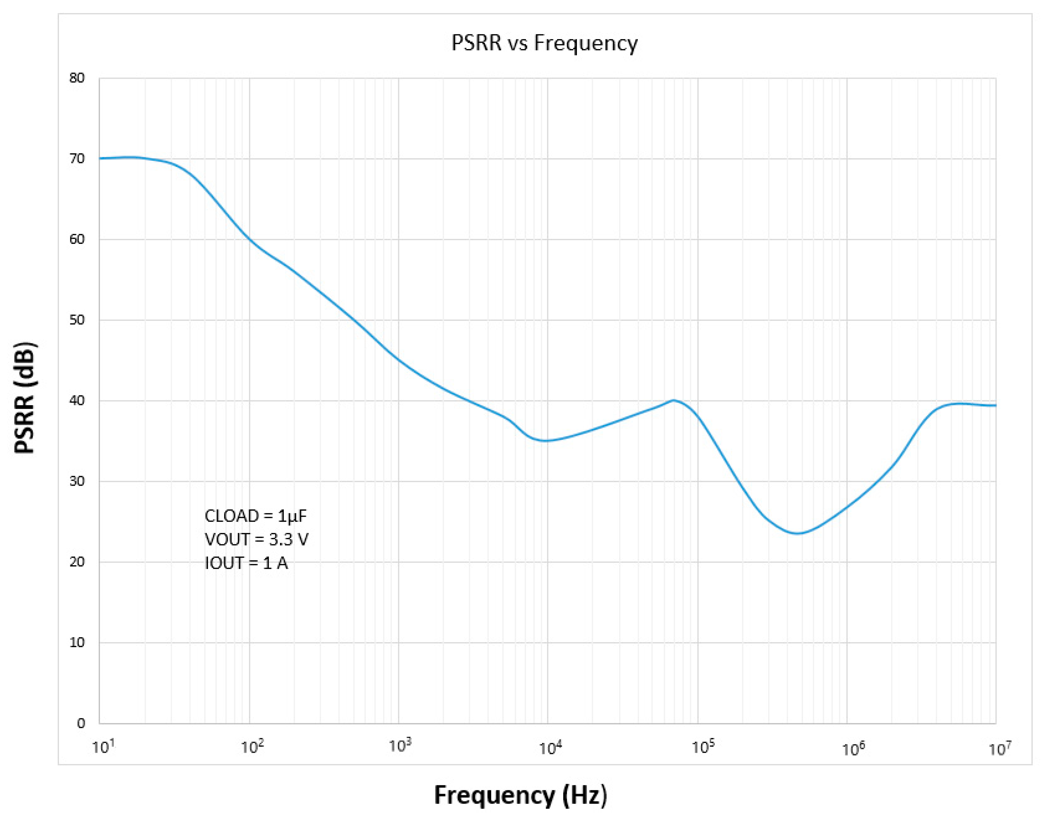
Figure 4 represents the PSRR characteristic of the TPS785-Q1 automotive high PSRR LDO [
14], which has its maximum PSRR of around 70 dB between 10 and 40 Hz. This value of PSRR is enough to consider it a high PSRR LDO, but the input voltage supply’s switching frequency is also vital [
11,
16,
17]. For example, the switching frequency of newer switching regulators is between 300 kHz and 6 MHz, and the LDO response time is too slow to efficiently filter out the switching noise, due to the fact that the noise is outside the bandwidth of most typical high PSRR regulators [
11,
18].
There are five regions represented in
Figure 4. The first region contains the frequency range from 10 to 40 Hz, where the PSRR has its peak (70 dB), and is approximately a flat curve. The frequency range 40 Hz–10 kHz, where PSRR decreases steadily at 20 dB/decade, forms the second region. In the third region (10–70 kHz) PSRR increases again to 40 dB. The fourth region sees a decrease in PSRR from 40 to 30 dB at 300 kHz. The first four regions are the effective PSRR bandwidth; thus, TPS785-Q1 has an effective frequency range between 0 Hz and 300 kHz. In the fifth region (300 kHz–10 MHz), the change in PSRR depends on the numerical value of the output capacitor C
OUT (
Figure 3) and its impedance, and the parasitic board impedance; thus, the LDO contribution to PSRR decreases.
The behavioral model of TPS785-Q1 provided by Texas Instruments is a PSpice Allegro library file [
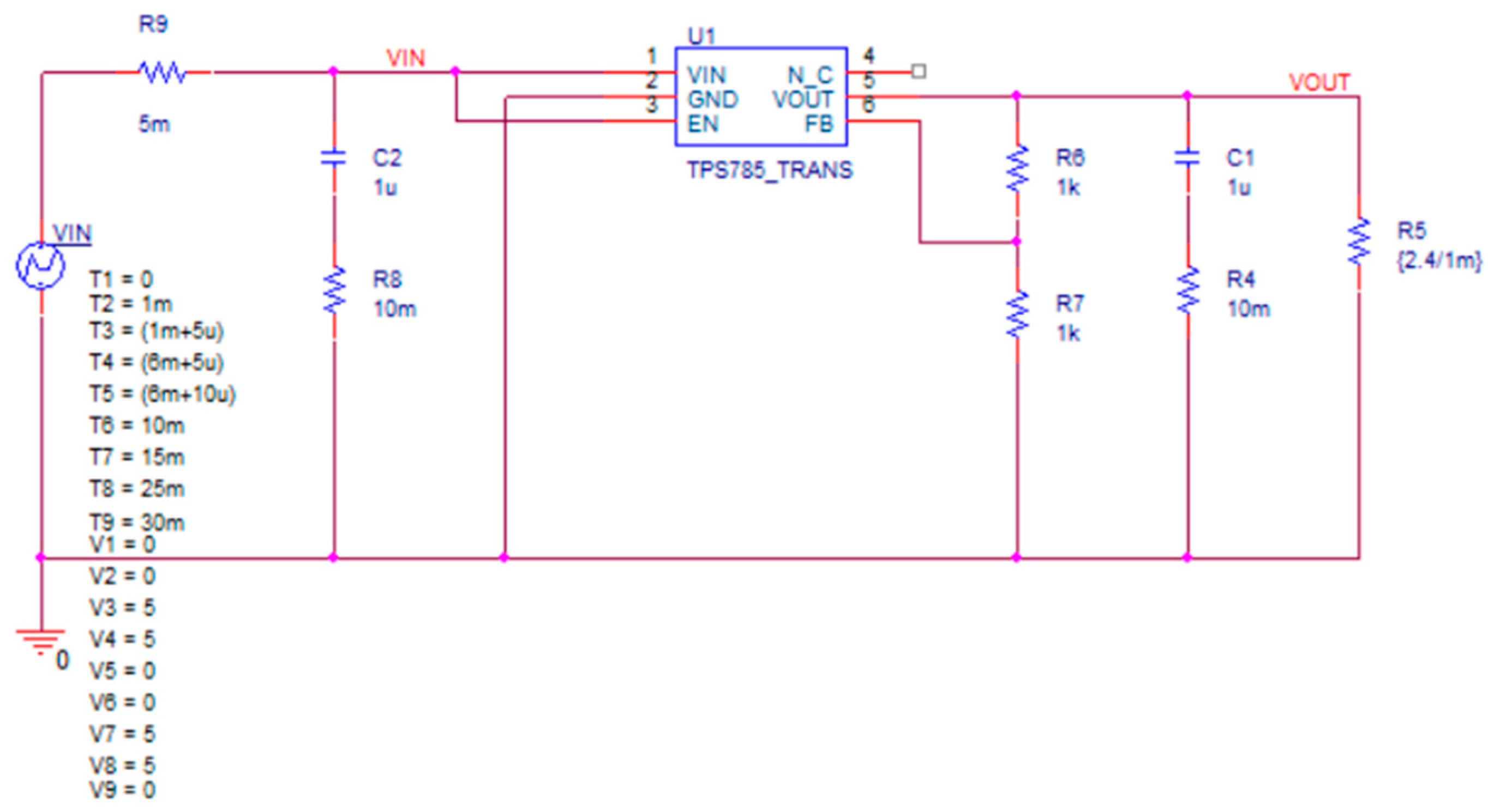
19]. We ran the model with the simple application circuit created in the OrCAD Capture CIS environment (
Figure 5). The output voltage was set at 2.4 V and the load current at 1 mA.
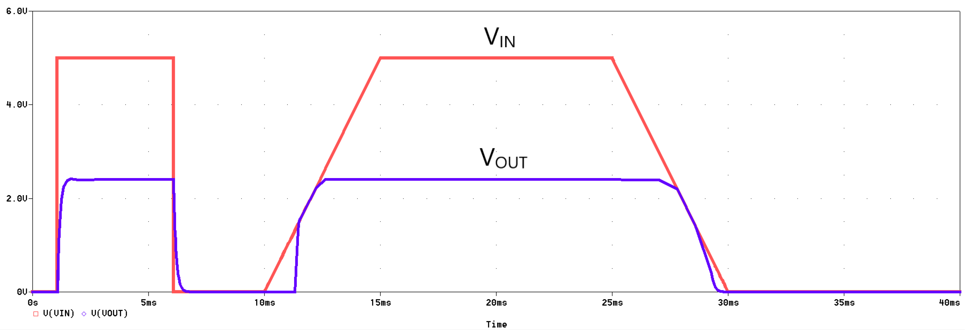
Figure 6 shows the results obtained using the demo application test-bench. In the beginning of the simulation, there is an abrupt 5 V pattern of the input voltage
VIN for both rising and falling edges (1–6 ms) and the output voltage
VOUT regulates at 2.4 V within a certain slew-rate. The second pattern shows slower slopes of the input voltage VIN for the rising and falling edges (10–30 ms). It can be noted that there is a certain threshold of the input voltage above which the LDO starts working.
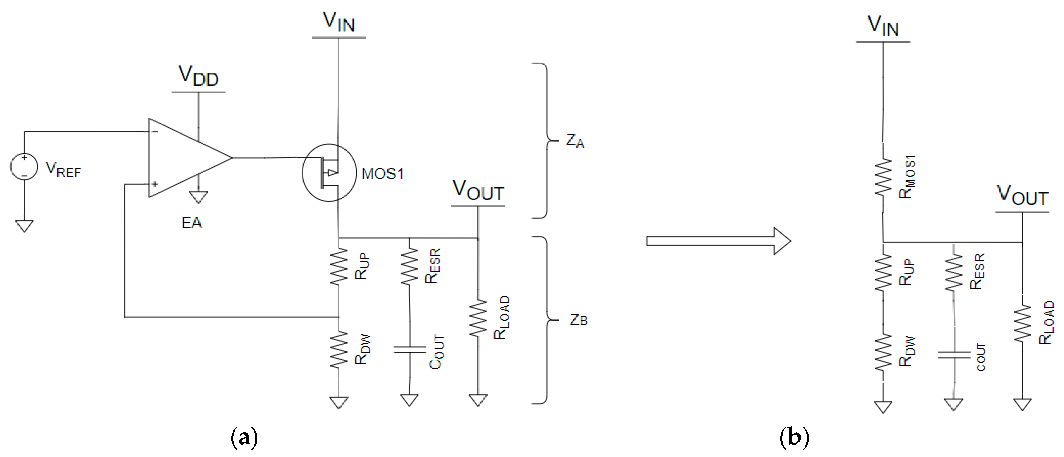
From the unencrypted library file, we found that this TPS785-Q1 model is a transient model, built for the PSpice Allegro simulator only, and is in its first version. The existing implemented characteristics are the following: start-up time, PSRR, enable/VIN shutdown, load and line transients, and internal current limit, and the model supports inverting the topology. In order to better understand how the PSRR model works, we further performed a reverse engineering of the library file code, so
Figure 7a represents the simplified concept of the TPS785-Q1 model, along with the general PSRR concept that is currently implemented [
11,
20]. It consists of the error amplifier EA, the reference voltage V
REF, the pass transistor MOS1, the feedback resistors R
UP and R
DW, the output capacitor C
OUT with its series resistance R
ESR, and load resistor R
LOAD. The components can be grouped into two impedances,
ZA and
ZB.
The PSRR can be calculated as it follows:
In the first region of PSRR vs. frequency characteristic from
Figure 4, the error amplifier has a large gain and this results in
ZA being well controlled, which translates into a high PSRR. In the second region, the gain of the amplifier starts dropping at 20 dB/decade. The sensitivity of the loop with respect to the changes in the output voltage decreases because the amplifier gain decreases; thus, the impedance of the transistor adjusts slower to the changes and this results in a decrease in PSRR. The impedance of the output capacitor decreases with the increase in the input signal frequency and this increases the LDO PSRR in the fifth region. The impedance
ZB decreases to the point where most of the signal is short-circuited across the capacitor instead of being attenuated by the LDO. In this case, where the LDO no longer contributes significantly to the PSRR, the pass transistor MOS1 is treated as a simple resistor and only attenuates the ripple passively [
11,
20]. This situation is revealed in
Figure 7b, which was drawn for high frequencies, and differs from
Figure 7a by eliminating the LDO and replacing the pass transistor MOS1 with a simple resistor R
MOS1.
We also simulated the PSRR characteristic of the already existing TPS785-Q1 model. The PSRR simulation test-bench is provided in
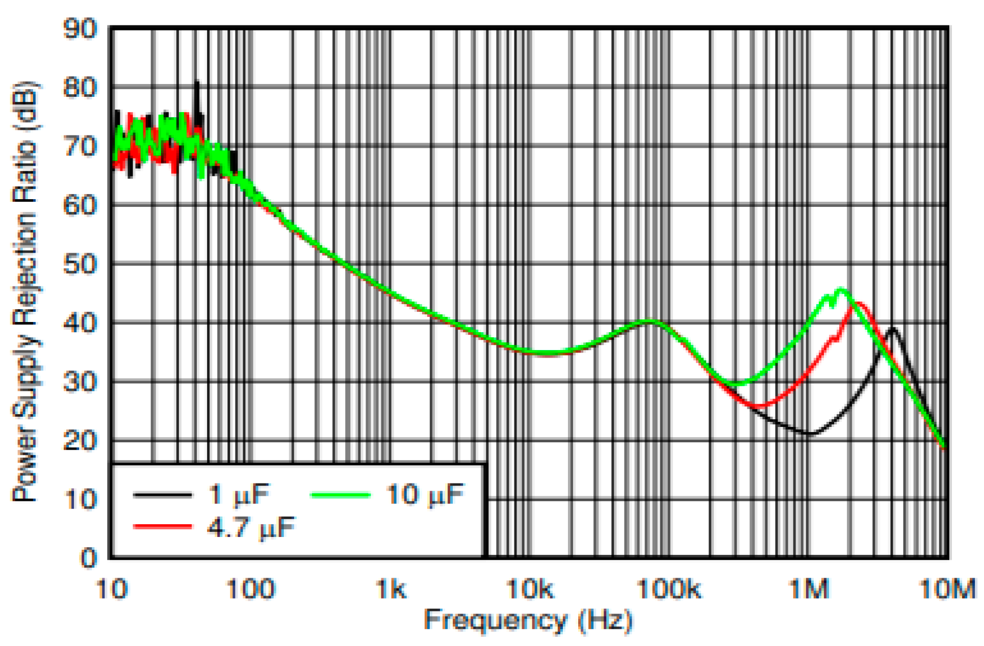
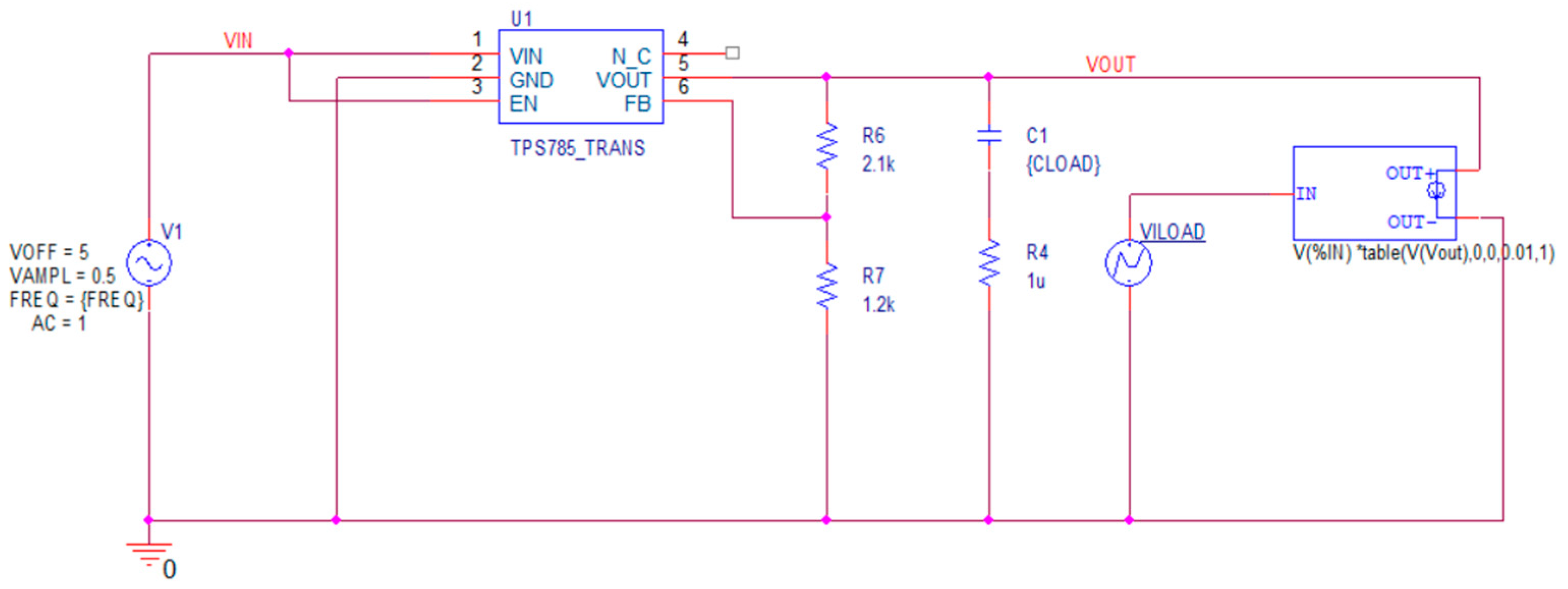
Figure 8.
The input voltage source VIN is a 5 V DC component on which a 1 V amplitude sine component modeling the additive noise is overlapped. The output voltage VOUT is set at 3.3 V and the load current is set at 1 A, as specified by the PSRR conditions. The load capacitor C1 is given three values (1, 4.7, and 10 µF) through parameter {CLOAD}, so three simulations were performed.
Figure 9 shows the family of simulated PSRR characteristics vs. frequency, having the capacitor C1 {CLOAD} from
Figure 8 as the parameter. Thus, the violet curve shows the 1 µF capacitor’s value, the red curve shows the 4.7 µF capacitor’s value, and the green curve shows the 10 µF capacitor’s value. Compared to the datasheet characteristic presented in
Figure 4, the flat region is at 60 dB instead of 70 dB, which represents a disadvantage of the old PSRR model given in [
14]. The capacitor influence is visible from around 1 kHz, whereas the datasheet characteristic sees a capacitor influence starting at 300 kHz.
3. Materials and Methods for the New Proposed PSRR Model Implementation
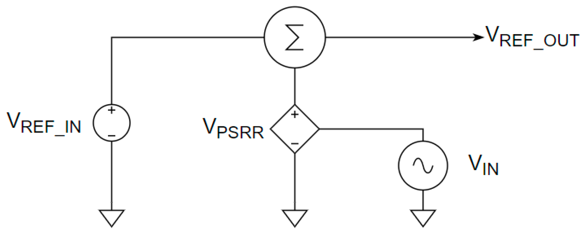
For materials, we started from the existing TPS785-Q1 model from Texas Instruments, from which we eliminated the old PSRR characteristic, and added our new PSRR concept, as shown in
Figure 10. For the method, we implemented the PSRR functionality by modifying the reference voltage V
REF_IN. The ideal reference voltage V
REF_IN of the LDO is added to the PSRR voltage source V
PSRR, which depends on the ripple of the input voltage
VIN and its frequency, and the result is V
REF_OUT. Then, V
REF_OUT is sent through the feedback resistors R
UP and R
DW (
Figure 7a), and yields the output voltage
VOUT and its variations (
Figure 7a).
In
Figure 10, the PSRR source V
PSRR holds the information about the input voltage source ripple Δ
VIN and frequency, which is demonstrated below.
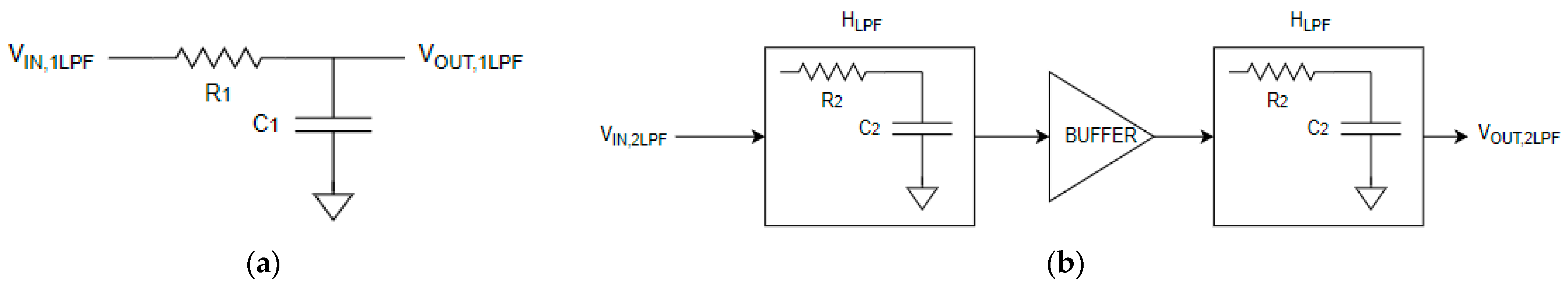
VIN is DC shifted and the DC information needs to be eliminated from the original signal. We used a first order passive low pass filter to determine the input signal
VIN frequency, and a second order active low pass filter to eliminate the DC component of
VIN. The first order low pass filter schematic is shown in
Figure 11a, and the second order active low pass filter concept is presented in
Figure 11b.
The transfer function of the first order low pass filter is:
where
ω =
2πf is the angular frequency, f is the frequency,
R1 is the low pass filter resistance value, and
C1 is the low pass filter capacitance value (
Figure 11a).
The transfer function magnitude of the first order low pass filter is:
and the transfer function phase of the first order low pass filter is:
Having a second order active filter in which the two stages are separated galvanically by a buffer, the total transfer function can be written as shown in Equation (6), based on relation Equation (3), with the magnitude and phase calculated in Equations (7) and (8). The components’ values are chosen to be equal due to the simplicity of calculations (
Figure 11b) [
21,
22,
23].
where the magnitude of the transfer function is:
and its phase is:
The cutoff frequency (where the magnitude of the transfer function drops to −3 dB) of the second order active filter is:
In order to achieve the DC component of the voltage VIN, we used relations Equations (6) and (7), in which we chose the resistance value R2 of 1 MΩ and capacitance C2 of 1 mF, which leads to f−3dB = 0.000160 Hz, i.e., a numerical value very near to 0 Hz.
Another challenge of modeling the characteristic PSRR vs. frequency is to determine the frequency of the input signal
VIN, by filtering the input ripple signal Δ
VIN, once again using a first order low pass filter, and then compute the root mean square (RMS) values of the input and output signals of the filter, V
RMS,IN and V
RMS,OUT [
24,
25]. We set the filter cutoff frequency to 40 Hz, where the PSRR characteristic starts dropping at 20 dB/decade from the flat region (
Figure 4). The cutoff frequency of the first order low pass filter is identical to that of the second order low pass filter, which uses the same values for the resistors and for the capacitors. In order to achieve this cutoff frequency, the filter resistor R
1 was set to 10 kΩ and, based on relation Equation (9), the resulting value of capacitor
C1 was 1.6 nF.
Since the signal at the output of the filter is phase shifted, the ratio of the instant values of the input and output signals of the first order low pass filter cannot be performed, but the RMS values are stationary, and their ratio V
RMS,IN/V
RMS_OUT reflects the signal
VIN frequency. The formula used for RMS calculation is:
where
T is the signal period and
v(t) is the time-varying signal.
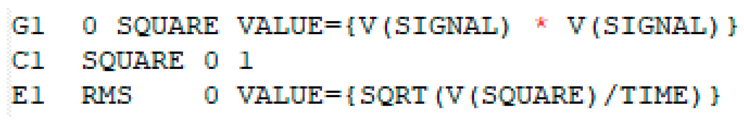
The implementation of relation Equation (10) in PSpice poses a challenge and cannot be performed directly. The time integral of the squared signal is computed by injecting a current having the value
v2(t) into a 1 F capacitor. Then, the value of time integral is divided by time and the square root value is extracted. The operating principle of the capacitor used for the implementation of the RMS formula is given as:
The principle of RMS code implementation from relation Equation (11) is given in
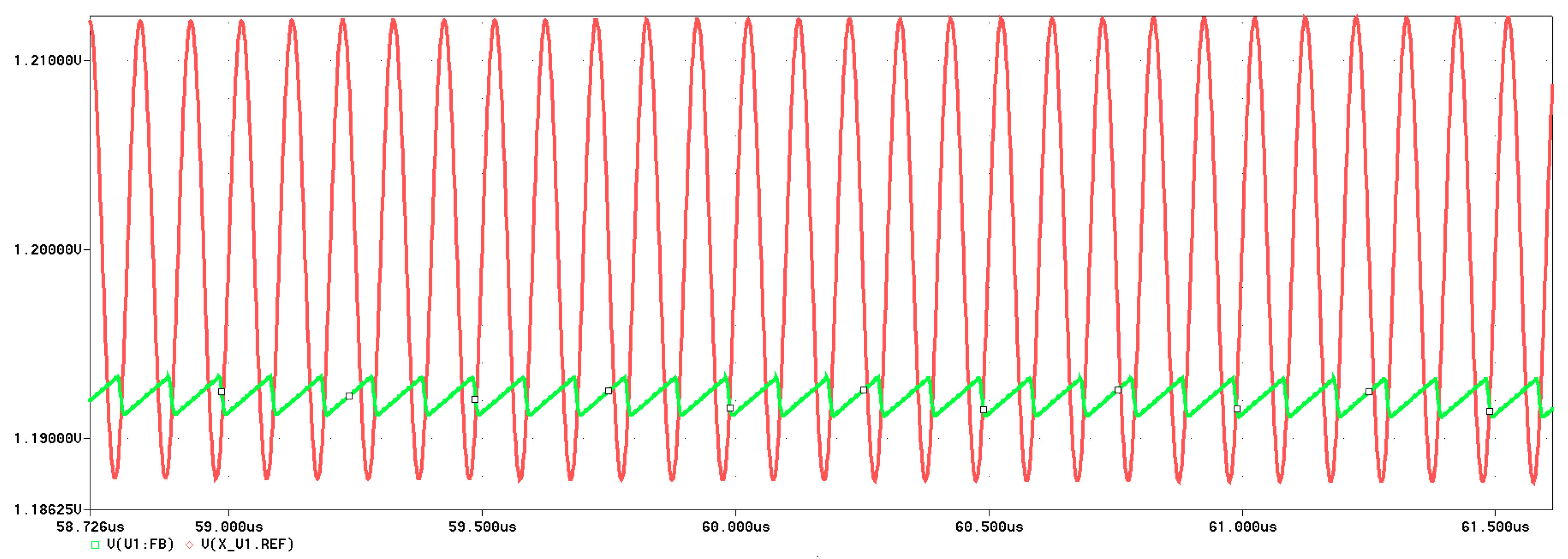
Figure 12.
The ratio of the RMS values of the input and output signals of the low pass filter is:
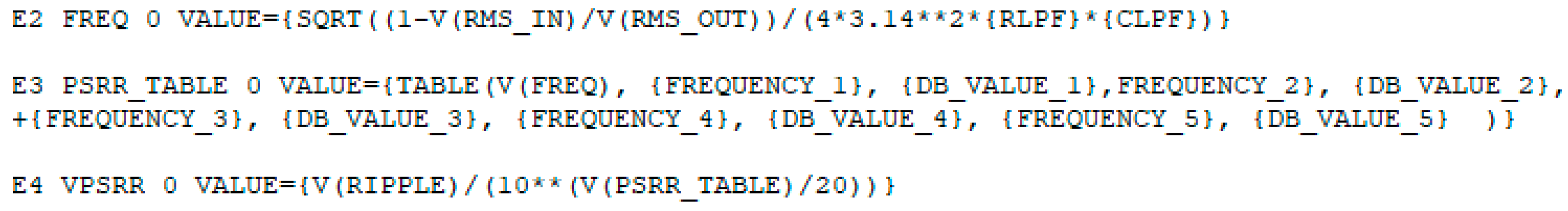
We associated a PSSR value in dB for each frequency of interest in PSpice using the TABLE function. The PSRR values between the two frequencies of interest are interpolated. In order to obtain a smoother PSRR vs. frequency characteristic, more frequency points were chosen.
The PSRR values in
dB from the PSpice TABLE need to be converted to numerical values as follows:
The final V
PSRR that is added to the ideal reference voltage V
REF_IN, and gives the output reference voltage V
REF_OUT (
Figure 10), is computed as:
The frequency computation, PSRR TABLE implementation, and V
PSRR determination in PSpice are presented in
Figure 13, in which relations Equations (12)–(14) were used.
6. Conclusions
In this paper, we proposed a new method for improving the PSSR response of automotive LDO behavioral models for frequencies below 500 kHz, which is based on mathematical relations combined with circuits’ relations.
We first used an existing commercially available automotive LDO model (TPS785-Q1 from Texas Instruments), which is available on Texas Instruments’ official website [
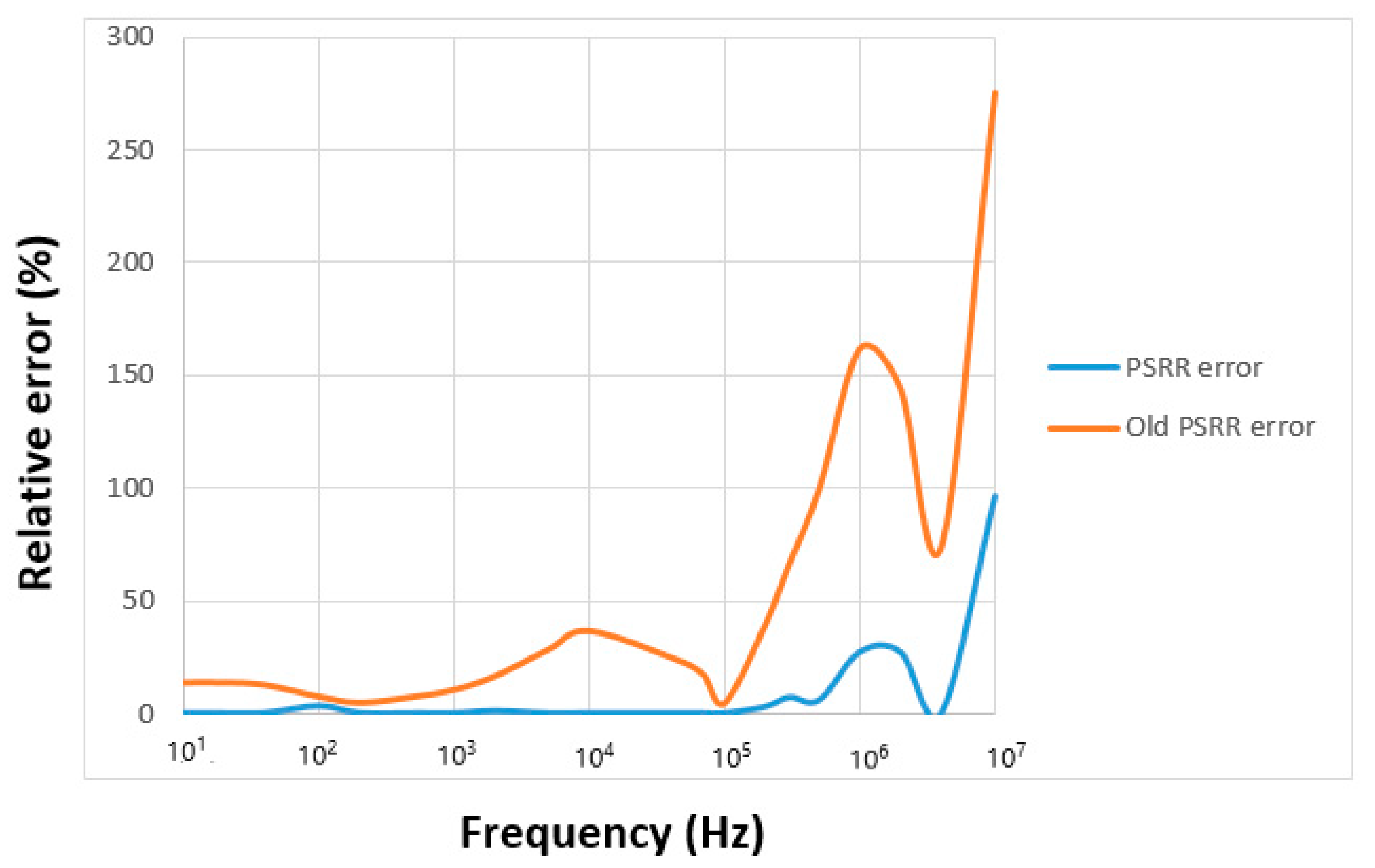
19]. We began by simulating the original model and plotted its PSRR characteristic, then we built a new PSRR model and integrated it into the LDO model, from which we eliminated the previous PSRR approach. The proposed method is not linear, so the PSRR characteristic was plotted using transient simulations. During the simulation phase, we noticed that the PSRR characteristic behaves extremely well at frequencies below 500 kHz, having an error lower than 7%, whereas for frequencies over 500 kHz up to 10 MHz, we concluded that the inaccurate behavior of the error amplifier greatly influences the PSRR response.
The implementation achieved in this paper proves extremely important in the automotive domain, in which simulations are usually chosen over real testing. Since the LDO is one of the most used power supply circuits in cars, this totally justifies the need for accurate LDO models. One of the most critical requirements of the LDO is the PSRR, which has not been explicitly addressed until now in circuit modeling. Most of the exiting commercially available LDO models show basic behavior and do not model the PSRR characteristic. Newer LDO models also include very simple PSRR functionality, but this is inaccurate and does not model the real characteristic properly over the functioning frequency range. Our work provides an optimized PSRR modeling method that models the real PSRR characteristic accurately for frequencies below 500 kHz, thus filling an important gap in the field. In order to accurately model the entire frequency range, the error amplifier also needs to exhibit accurate behavior, and this error amplifier redesign represents a future research direction.
Other future research directions consist of the enhancement of the current PSRR approach to also support variation with the load capacitor. The ripple of the output current needs to be measured using the same methodology as for the output voltage presented in this paper; the current ripple frequency using the RMS integration should then be determined, and another variation added to the existing one.


