1. Introduction
In order to improve performance, hardware architects have aimed to increase computer clock frequency; moreover, they have enhanced the instructions per cycle (IPC) coefficient by increasing the number of instructions that are completed in a clock cycle. For this to be accomplished, it is necessary to implement multi-stage assembly lines and then execute multiple instructions in parallel, thus obtaining a superscalar architecture. The main problem that arises from using a pipeline or multiple pipelines is maximizing the use of each stage of the assembly line [
1,
2]. To address this problem, architects have proposed and created complex mechanisms for executing instructions in a different order, thus increasing the complexity of the entire processor while maintaining power consumption within acceptable limits. An alternative to this problem, which allows for a high degree of parallelization at the instruction level, is a technique called multithreading. In essence, the instruction flow is divided into several fluxes named threads, so that these threads can be executed in parallel. A variety of multithreading projects based on different architectures [
3] have been realized and implemented in experimental [
4] and even commercial projects.
Programming languages often hide the instruction set architecture (ISA) and do not pass the predictability test because they do not express the temporal properties of the assembly language used. In addition, real-time operating systems (RTOSs) do not pass the predictability test because they hide the complexity of concurrent synchronization and communications between tasks, thus hiding the temporal delays generated by this orchestration. As a result, it is often desirable to determine real-time behavior using a test and evaluation software benchmark. Task contexts’ saving and restoring operations are also important issues when working with real-time kernels. Information regarding the tasks of an operating system is stored in data structures called task control blocks (TCBs). These TCBs must contain all the necessary parameters for creating the tasks and the necessary information for managing them.
RTOSs are primarily used for their accelerated response capability. A real-time scheduler is a program unit that controls execution and temporary preemption and completes the execution of some program modules based on a predefined algorithm to meet the required time constraints. Hardware schedulers and HW RTOSs [
5] are designed to relieve the processor from task scheduling overhead, enabling a worst-case execution time (WCET) to be specified [
6]. The preemptive schedulers introduce fluctuations in task execution times, degrading the performance of the RTS. A major drawback of non-preventive software scheduler implementations is that they introduce an additional blocking factor for high-priority tasks. Nevertheless, there are several important advantages when adopting this type of scheduler. Current benchmarks assess the accuracy of running programs without considering how long it takes to execute certain instruction sequences.
This paper begins with a brief introduction, and then
Section 2 compares the proposed implementation with that of other similar projects.
Section 3 and
Section 4 present the real-time event handling based on a hardware RTOS architecture and the integrated hardware scheduler.
Section 5 describes the implementation of the proposed architecture using the Virtex-7/Nexys 4 DDR development kit, also presenting the resource requirements for implementing the processor using Verilog HDL.
Section 6 and
Section 7 present the discussions, conclusions and future directions of research.
2. Related Work
The authors of the present paper aimed at a realistic comparison between different CPU architecture implementations. The XMOS processor presented by May in [
7] has a scalable architecture, so it can use the entire central processing unit even if the number of active execution threads is less than four. The new XMOS architecture allows designers to build systems with multiple Xcore kernels connected. Communication between Xcore cores from the same chip or different chips is performed using messages sent through point-to-point communication links, ensuring the predictive execution of concurrent programs. The cores interact with other external devices via integrated ports. Therefore, the XMOS architecture can be used successfully to build multi-core systems, dedicated boards or distributed systems. The processor core proposed in [
8] is composed of two distinct pipelines. The first one is dedicated to a single hard real-time (HRT) execution thread, and the second pipeline is dedicated to non-HRT (NHRT) execution threads. As can be seen from the example presented by the authors, in a quad-core version, each core is composed of four hardware slots. Thus, each core can simultaneously execute an HRT thread and three NHRT threads. The HRT thread is assigned the highest priority, being isolated from the other NHRT threads in the core through the real-time scheduler. The threads’ priorities are fixed, and round-robin is the chosen scheduling scheme. Each kernel is composed of two scratchpad memories, one for data and the other for instructions (D-ISP and DSP) and ensures data integrity by individually assigning a subset from a bank cache to each task [
9]. To minimize interference between tasks, the authors of this paper propose using an analyzable real-time memory controller. The disadvantage of this project is the increased resource requirements and rigidity because every core can only have one HRT thread and an arbitrary number of NHRT threads.
In [
10], Clemente et al. present a special implementation of a run-time hardware scheduler designed for reconfigurable systems. The authors designed and validated a run-time scheduler that operates with task graphs. The task graphs are analyzed at design time and the information extracted is used at run-time in order to obtain near-optimal scheduling operations. The performance of implementing this scheduler in hardware applies to all optimization techniques while introducing a delay of only a few clock cycles. The experimental results presented in this paper prove that the proposed scheduler outperforms conventional run-time schedulers based on as-soon-as-possible techniques. In addition, our scheduler provides efficient management of the execution of task graphs for reconfigurable multitasking systems, which can significantly improve the performance of the system and also reduce energy consumption. In other architectures [
11], architects focus on designing flexible processors for embedded applications, reducing energy consumption and improving speed and design time. Vermeulen et al. proposed a novel hybrid CPU architecture [
11] that allows the implementation of time-critical functionality on a custom accelerator, thus preserving the flexibility of the platform implementation. To solve the data transfer and storage bottleneck for multimedia applications, a customized memory architecture is shared with the flexible component. The MIPS processor core proposed by Gschwind et al. in [
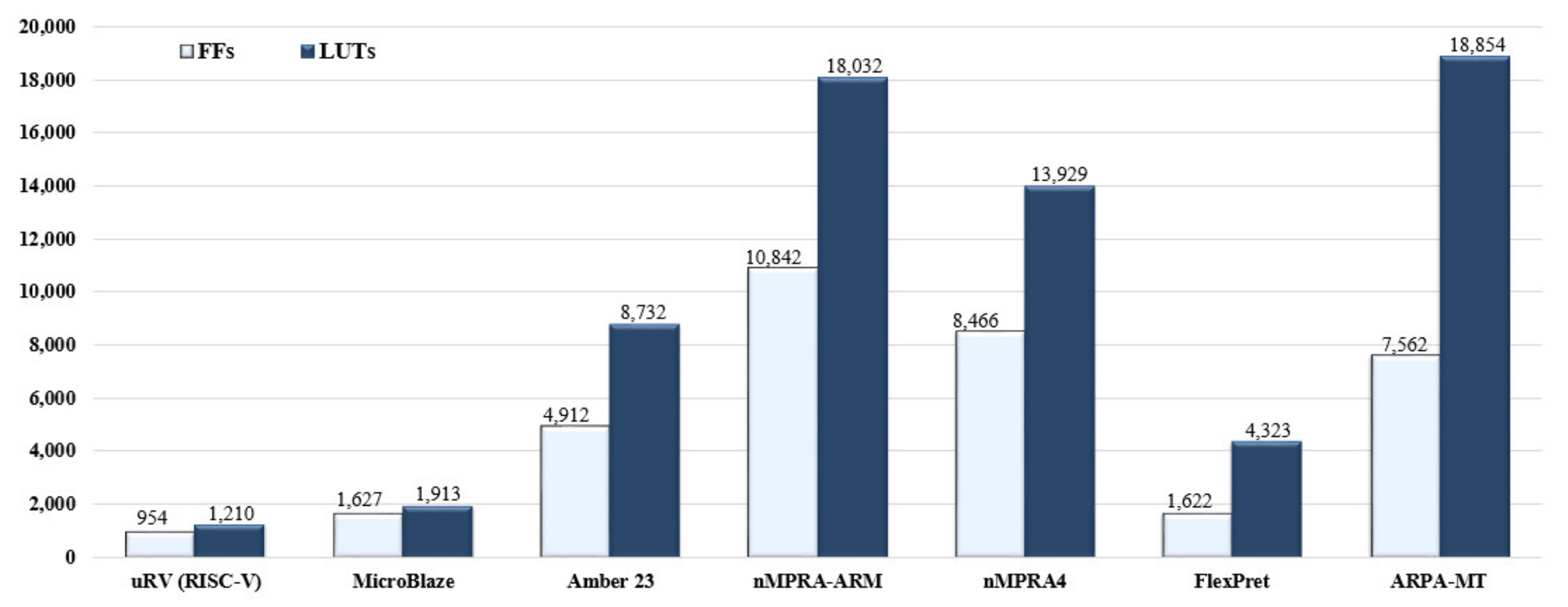
12] represents an FPGA application-specific processor prototype designed for embedded applications. The project was developed using the MIPS-I ISA architecture and the VHDL hardware description language. The authors design a reconfigurable MIPS processor core to support hardware/software co-evaluation of instruction sets for design space exploration. Therefore, we can see that with the arrival of high-density FPGA devices, prototyping has become accessible to the designers of integrated applications built around application-specific processors. Besides the MicroBlaze [
13] and Amber 23 processors [
14,
15] (
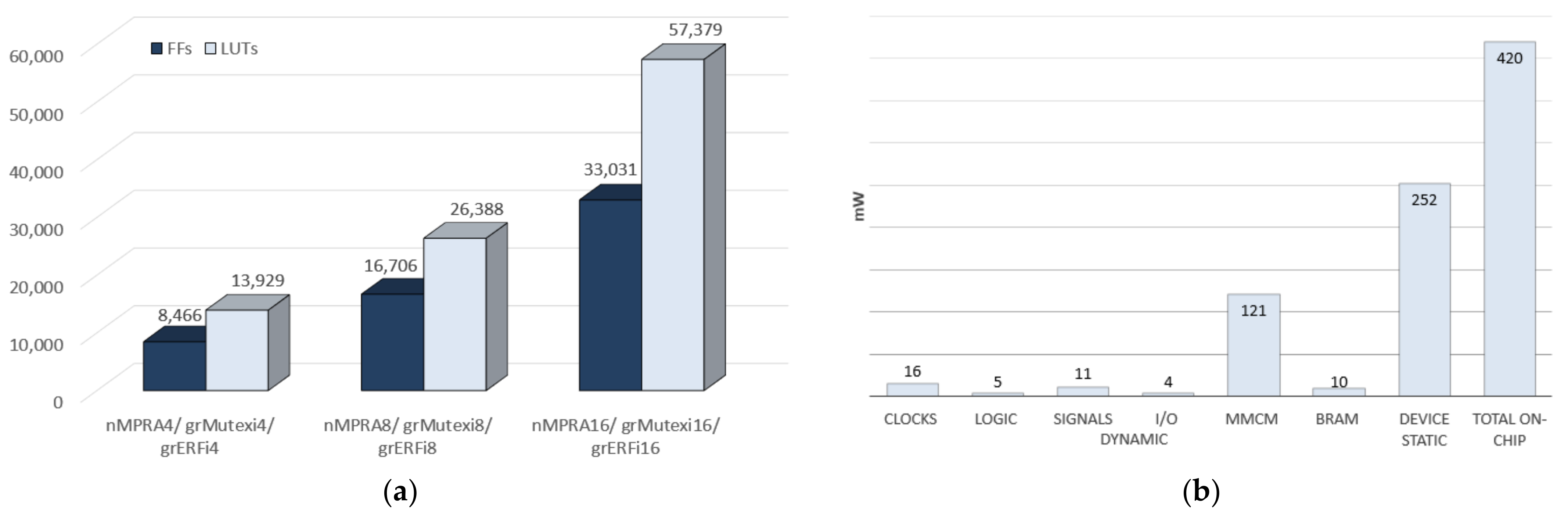
Figure 1), all processor implementations taken into consideration use complete or partial resource multiplication for 4 sCPUs/tasks/threads/contexts. The results obtained by the designers are related to the architecture of the implemented processor [
16,
17,
18,
19], with a particular impact on the data presented in the graph in
Figure 1.
3. Real-Time Event Processing Based on Hardware RTOS Architecture Support
The proposed concept is based on a five-stage pipeline assembly line and the multiplication of pipeline registers, program counter, GPR and each memory element on the datapath (such as flip-flops associated with the condition indicators, the sequential machine in the division unit and the flip-flops in COP0, etc.). An instance of the CPU will be referred to as a semi-CPU (sCPUi for task
i). Such a hardware instance comprises its program counter register, pipeline registers, GPR and its control registers. Therefore, the sCPUi runs the instructions of task
i (
i = 0, …,
n − 1) based on the nMPRA concept (multipipeline register architecture, where
n is the degree of multiplication) [
6]. The HW_nMPRA_RTOS project (nMPRA + nHSE) presented in this paper has been designed using the MIPS32 Release 1 ISA. MIPS (microprocessor without interlocked pipelined stages) provides the user with a system of coprocessors for extending the functionality of the basic CPU. Coprocessor 2 (COP2) is available to the user, so this research project consists of a system-on-chip (SoC) implementation of nMPRA and nHSE at the level of MIPS32 COP2, with the scheduler registers being explained in detail in the specifications of the nMPRA processor. The requirements of a hardware-implemented RTOS must comprise (but not be limited to) the following: guaranteeing a high level of real-time performance, quick interrupt (event) response, fast task context switch and application programming interface (API) execution, increased predictability and much lower CPU resource usage. In the proposed architecture, named HW_nMPRA_RTOS, each task has an associated timer that can be configured to generate an event when the time allowed for that task is nearing completion. Each hardware block is composed of three timers, one representing the recurrence period of the task that might generate an event at the specified time frame, and the following two timers representing the implementation of two deadlines. The first one is a soft deadline that can be an alarm, whereas the second is a hard deadline, equivalent to a fault.
The main contribution of this paper is a novel hardware scheduler that includes support for RTOS kernels (HW_nMPRA_RTOS), aimed at achieving worst-case latencies in the order of nanoseconds for the FPGA-based project. As a derivative contribution, we have implemented the structure of a hardware RTOS for MIPS32-COP2 in order to add predictive scheduler behavior and minimize kernel latency. The implementation of HW_nMPRA_RTOS comprises a real-time hardware operating system that achieves excellent performance at a low cost compared to conventional RTOS software implementations. Compared to simultaneous multithreading (SMT) processor designs, the current implementation only executes one sCPUi at any one time. HW_nMPRA_RTOS cannot run both sCPU0 and sCPU3 simultaneously because there is no multiplied ALU unit or condition testing unit. We have a single data memory and a sign extension unit (all combinational parts), etc.
The application field includes many automotive and robotics applications for which the overhead of commercial off-the-shelf CPUs is too high. Considering that FPGA vendor-provided cores, such as Microblaze and Nios, are not portable and have no sources available either, our HW_nMPRA_RTOS architecture favors an FPGA footprint and determinism of execution over performance, with code and data stored in the internal FPGA RAM. The hardware real-time event handling module validated in this paper is based on the CPU resource multiplication concept patented in Germany, Munich (DE202012104250U1) [
20].
The development of this circuit in Verilog HDL transforms the processor code representing the RTL level into a variety of other equivalent visual representations. Thus, using the RTL Netlist, Schematic and Graphical Hierarchy options, the processor can be viewed at different design stages. These options also provide the ability to debug and verify by using the cross-select property. The process of synthesizing the project represents the next step in the FPGA implementation. It involves transforming the project from RTL into logical gate representation. This means that the result from the Verilog code, together with the standard UNISIM libraries, is the non-logical gateway, containing primitives such as flip-flops (FFs) or look-up tables (LUTs). The next step in the validation of the proposed processor is the implementation of the project in the Virtex-7 FPGA circuit. This process consists of placement and routing operations, which, along with the corresponding algorithms, put the netlist elements into the FPGA circuit and connect them so that all requirements are met. This step may be quite slow, especially when using hardware debugging tools such as ChipScope Analyzer.
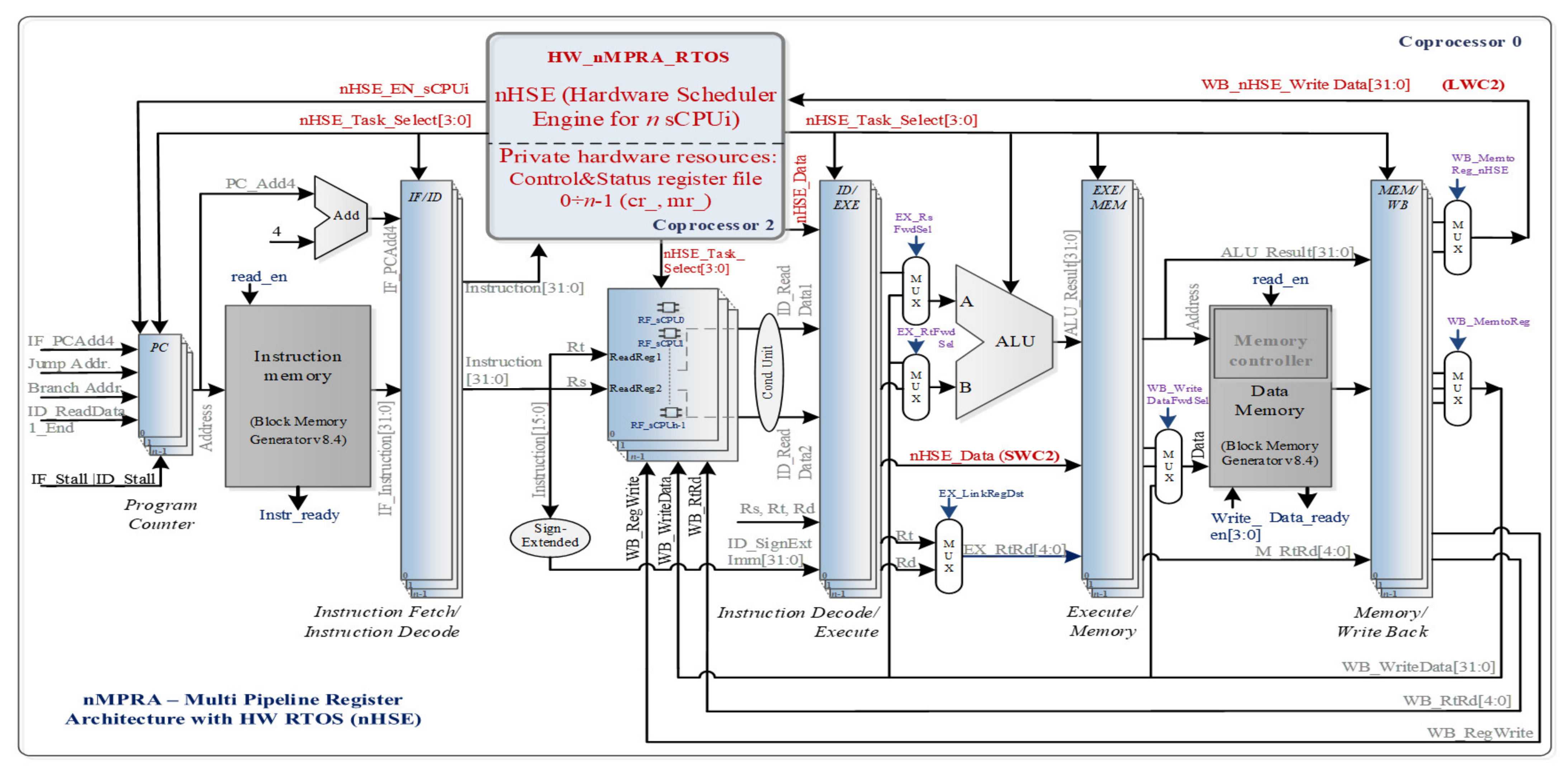
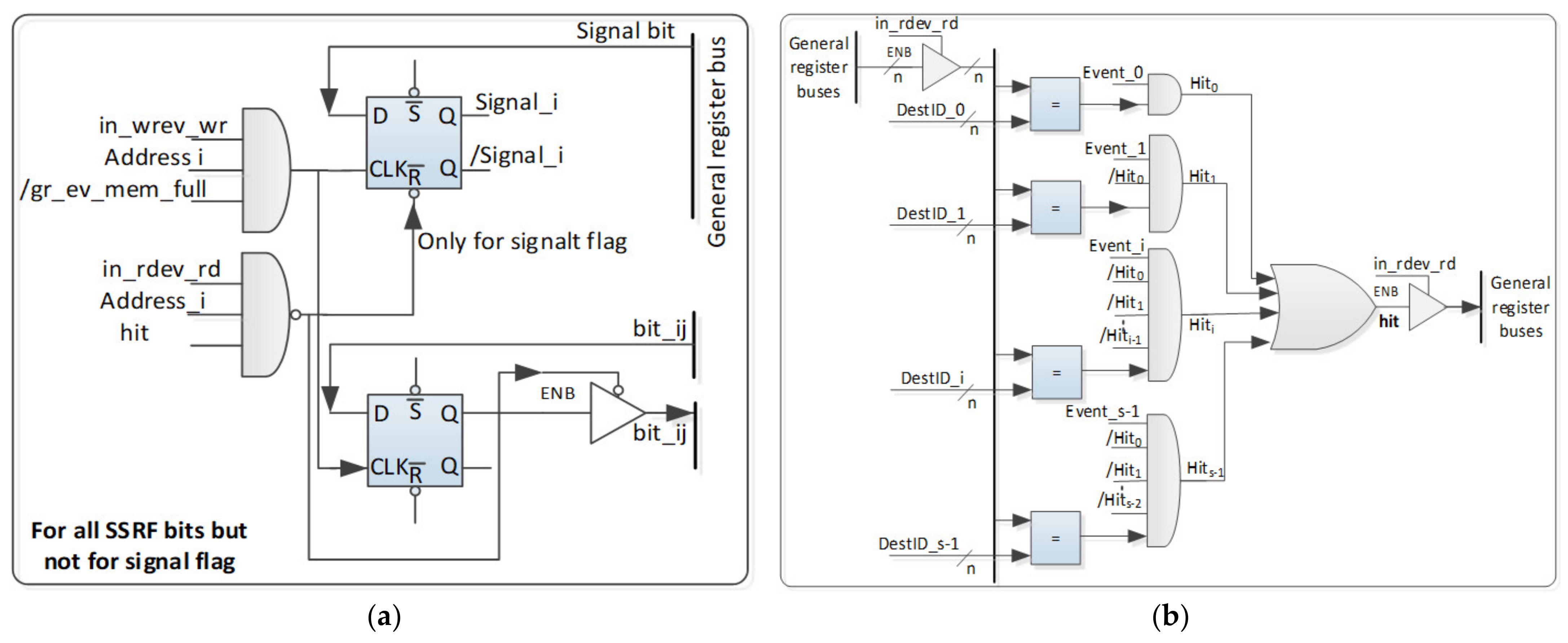
It is a known fact that the MIPS architecture assigns COP2 for user-specific implementations. COP2 has its own register file (RF), but it is transparent to the programmer due to the real-time event handling module. There are six COP2 instructions that are used to access local and global nHSE registers. The data transfer between nHSE, GPR and data memory is achieved by using the instructions implemented at the level of COP2, namely, CFC2 (copy control word from coprocessor 2 to GPR, opcode = 010010), CTC2 (copy control word from GPR to coprocessor 2, opcode = 010010), MFC2 (move word (mr) from coprocessor 2 to GPR, opcode = 010010), MTC2 (move word (mr) from GPR to coprocessor 2, opcode = 010010), LWC2 (load word from data memory to COP2 from data memory, opcode = 110010) and SWC2 (store word from COP2 to data memory, opcode = 111010).
Figure 2 shows the datapath effect of COP2 instruction execution, based on the nHSE module (hardware scheduler engine for
n threads). Thus, the block diagram indicates the datapath corresponding to the LWC2 instruction type that loads a word from the data memory into the hardware scheduler register, and the SWC2 instruction stores a word (control register abbreviated further as cr) from the hardware scheduler in the data memory. By executing a code sequence written specifically for validating the real-time event handling unit, the datapath presented in
Figure 2 will be tested, even in the case of a hazardous situation.
Figure 2 is an architectural diagram, and the Vivado implementation differs essentially from this architecture both in the way the code is written and in the internal structure of the FPGA circuit, optimally used by the Verilog compiler.
By the validation of the COP2 dedicated instructions, all registers associated with the hardware scheduler can be written or read in GPR space. Changing the number of sCPUi, interrupts, or mutexes does not entail the multiplication of instructions dedicated to the real-time scheduler. The multiplication of monitoring (mr) and control registers at the level of COP2 contributes to the total number of resources required to implement this processor architecture. The advantage of this is the existence of separate contexts for each sCPUi, thus resulting in an additional speed boost that comes from eliminating the need to save and restore parameters on the stack. The hardware scheduling unit is designed to activate only one of the
n sCPUis at a given moment. Efficiency is another feature that RTS needs to acquire so the real-time scheduler can satisfy all requests for task execution of a scalable system with limited hardware resources. In this context, it can be said that an RTS must be robust and safe, even in those situations where requirements reach their maximum points. The purpose of this project is to ensure the proper functionality of the process, even if the results produced after the deadlines are still used in some RTSs. Although tolerance to errors is another important aspect of the RTS, the scheduler must not allow the existence of unpredictable situations that may affect the safety of a human operator or even of the product beneficiaries. Compared to a general-purpose operating system, an RTOS typically uses round-robin scheduling to ensure the accuracy of real-time task processing. The earliest deadline first (EDF) algorithm can also be used to schedule an independent set of preemptive and aperiodic tasks that run on a single-core system. For this, each task τi is characterized by a WCET marked with Ci, a deadline Di, an execution period Ti and a Pi priority, used to select which of the ready-to-run
n tasks can be scheduled. A lower value for Pi represents a higher priority for the respective task, as follows: ∀
i|1 ≤
i <
n: Pi < Pi + 1. The smaller number of task context switch changes in EDF is a direct consequence of assigning dynamic Pi priorities according to the earliest deadline, independently of task periods (Ti). A periodic set of
n tasks can be scheduled with the EDF algorithm as follows (1):
The downside of the interrupt scheduling system in most current microcontroller applications is that it allows a large jitter in scheduling high-priority tasks. However, the possibility of executing out-of-core interrupts relieves the processor of additional overhead, thus eliminating several unnecessarily used context switches, including certain interrupt-specific clock cycles. The time required to change task contexts is the most significant factor in any RTOS. In the case of real-time systems, another workload factor is the time period required for the processor to execute the interrupt handling routine. If Q is the system tick and σ is the WCET corresponding to the periodic task, the overhead introduced can be calculated as the utilization factor Ut obtained by Equation (2).
For some RTSs, the preemptive CPU scheduler can be disabled for certain time cycles during the execution of the interrupt service routine (ISR). To achieve maximum performance, i.e., an IPC close to 1.0, it is necessary to modify the instruction and data memory handshake. The real-time event handling module provides the infrastructure that the applications need to dynamically monitor the task execution time, handle interrupts and count unallocated CPU cycles. This module can also be used for debugging and monitoring the timing behavior of each sCPUi, thus improving the performance of the hardware RTOS and offering low interrupt latency.
4. Preemptive Real-Time Scheduler Architecture and FPGA Implementation
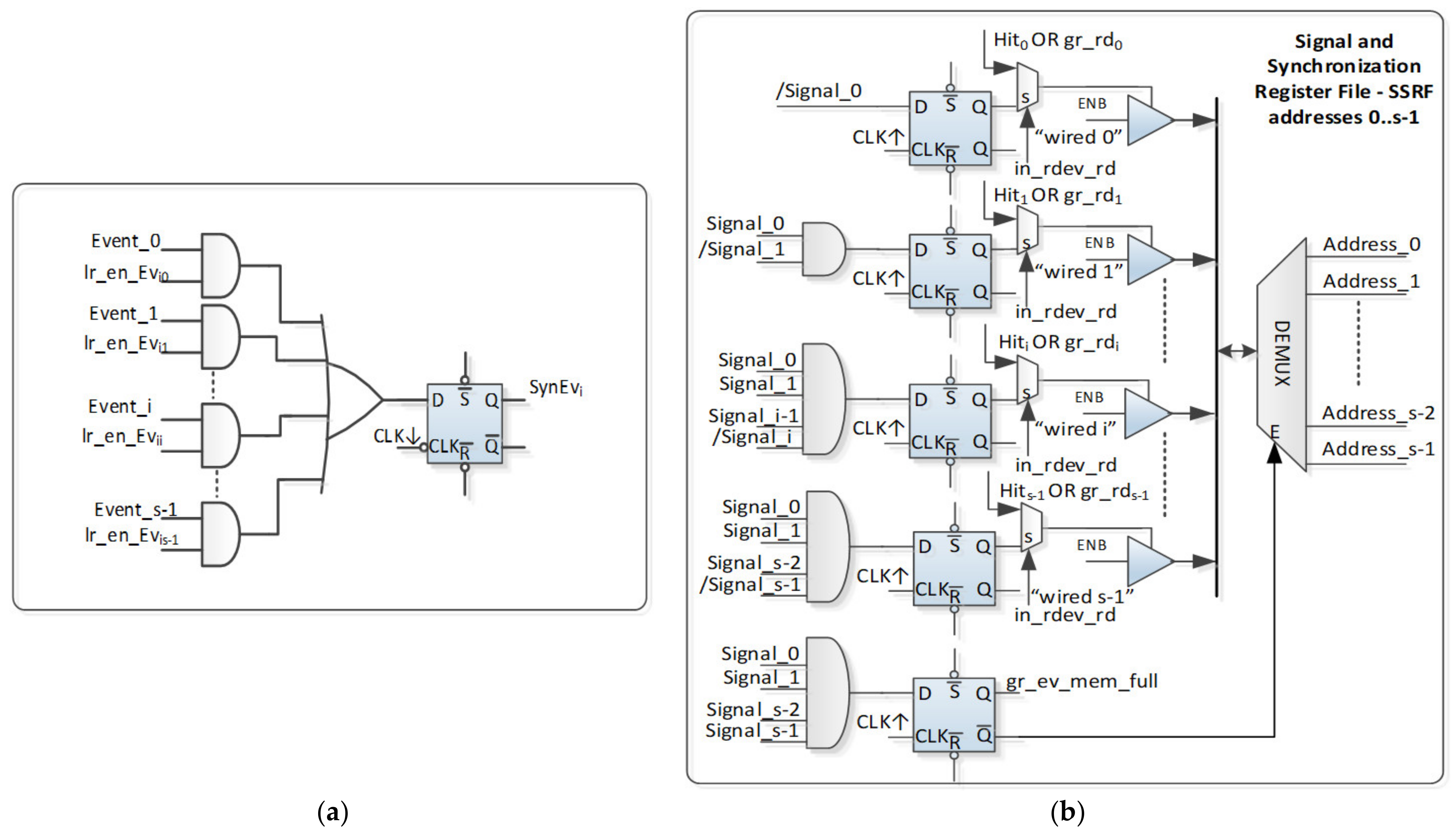
This section describes the architecture of the hardware scheduler and its internal structure (see
Figure 3). The real-time event handling unit is a scalable module based on the Mealy finite-state machine (FSM), which can be successfully used even in real-time applications. The contributions of this work are the result of theoretical and practical research in real-time scheduling. In this context, extra attention was paid to minimizing the overhead due to the operating system, allocating the time to the software scheduler and context switching, reducing the overall jitter effect. The proposed processor concept described in this paper is based on the five-stage pipelined MIPS processor [
21,
22] proposed in [
23,
24]. For implementing the new COP2 instructions, we used the MIPS32 instruction set. Possible sCPUi events are as follows: timer (TEvi), watchdog timer (WDEvi), deadlines (D1Evi and D2Evi), interrupts (IntEvi), mutexes (MutexEvi), inter-task communication events (SynEvi) and self-sustaining execution for the current sCPUi (lr_run_sCPUi). The abovementioned events can be validated with local registers (lr) en_Ti, en_WDi, en_D1i, en_D2i, en_Inti, en_Mutexi and en_Syni signals, the only exception being run_sCPUi. These signals must be stored in a special register named the task register (crTRi). The current nHSE scheduler is based on priorities. In addition to the watchdog timer registers (mrWDEVi), deadline 1 and deadline 2 (mrD1EVi, mrD2EVi), the effective monitoring registers (mrCntRun, mrCntSleepi, mr0CntSleep) are implemented in the hardware at the level of each sCPUi. sCPU0 can access monitoring registers and can implement other scheduling algorithms via software. The sCPUiEvi signal, which is used to signal the occurrence of an expected event, is enabled by the stop_CPUi signal. The scheduler register-transfer level (RTL) equations are the following (“∧” AND logic, ”∨” OR logic, “/” NOT logic, “CLK” HW_nMPRA_RTOS processor clock, “
” positive edge trigger):
The FSM outputs (Oi) are dependent on the scheduled sCPUi IDs and also on the current inputs represented by the events in
Figure 3.
The block diagram contains the sCPUi_ready functional blocks and the register that stores the ID of the highest priority sCPUi (see
Figure 3). Subsequently, the AND gate and the D flip-flop are activated when there is no other active sCPUi. The
Figure 3 block shows the ID register of the active sCPU together with the synchronization logic, the static scheduler, the dynamic scheduler and the block related to the events. The en_CPU signal can be used mainly for power saving. The activation or deactivation of any sCPUi specific resources can be accomplished with O0 (en_pipe_sCPU0) through O
n-1 (en_pipe_sCPUn-1) signals. The proposed schematic can be used for static scheduling if each task runs on a sCPUi. In this case, the static priorities are identified by the IDs of the tasks. In this context, interrupts borrow the priority and the behavior of the task. Thus, interrupt behavior is much more predictable in the context of a real-time application (a task can only be interrupted by interrupts attached to a task with a higher priority).
6. Discussion
The HW_RTOS_nMPRA dynamic preemptive scheduler is responsible for deciding which task to select for the RUN state, thereby making the appropriate context change; attaching interrupts; counting the clock cycles used by each sCPUi separately; counting unused clock cycles; managing the two time limits for the tasks; the transition of tasks from the RECEIVE state to the READY state at the expiration of the time periods set for each. Thus, the scheduler selects for execution the highest priority sCPUi from those in the READY state. In other words, the task chosen for execution is the highest priority task based on priorities (mrPRIsCPUi). RECEIVE or PREEMPTED tasks are not enabled for execution.
The resource requirements for implementing the proposed hardware scheduler based on real-time event processing and the low power consumption make it ideal for Internet of Things applications requiring flexible processing of data streams generated by multiple sensors, thus providing scalable, flexible solutions at the highest quality standards. Even RTLinux [
29], a commercial RTOS, has a 32 µs jitter for the scheduling operation (worst-case jitter for a Compaq iPAQ PDA based on a 200 MHz StrongArm).
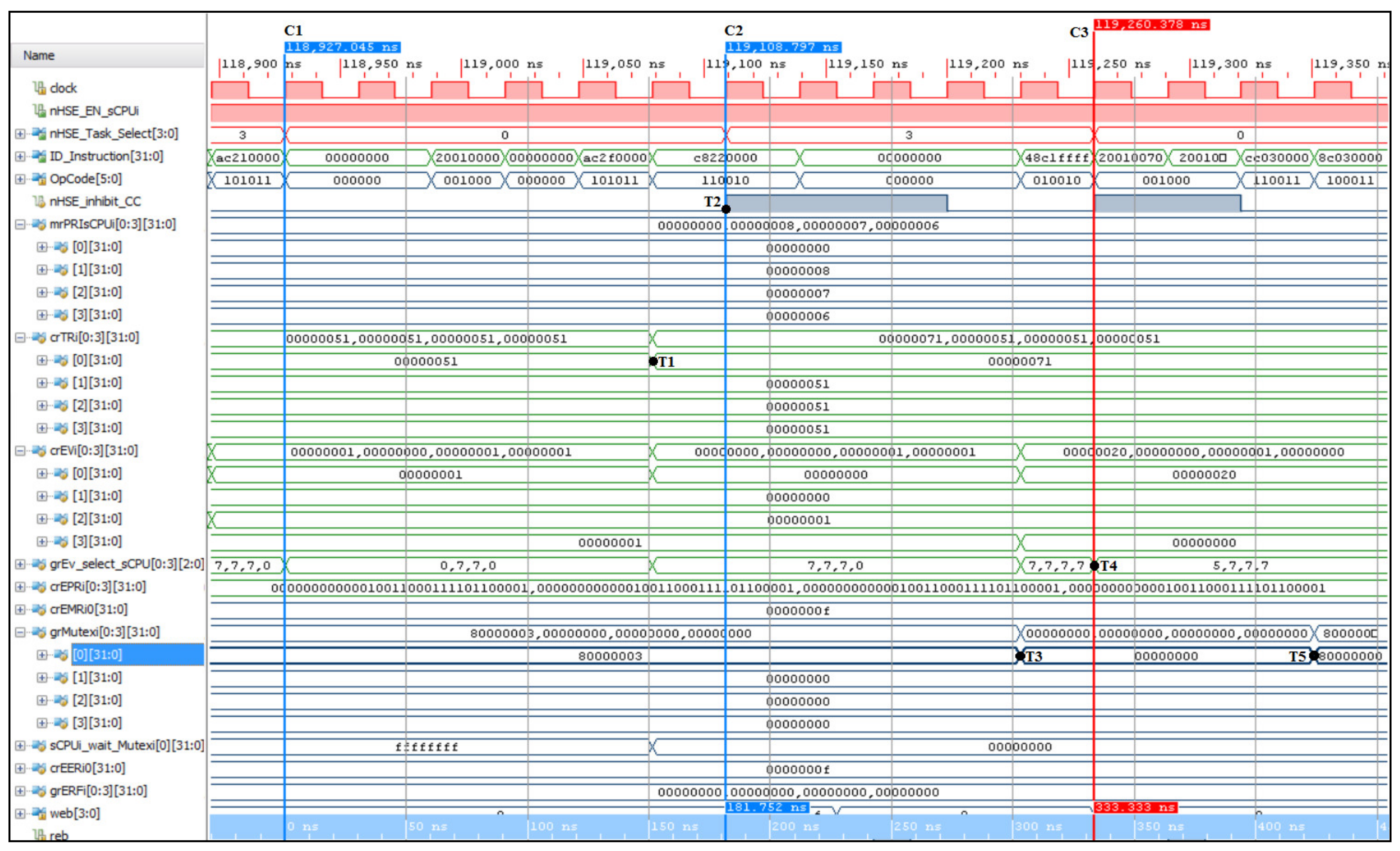
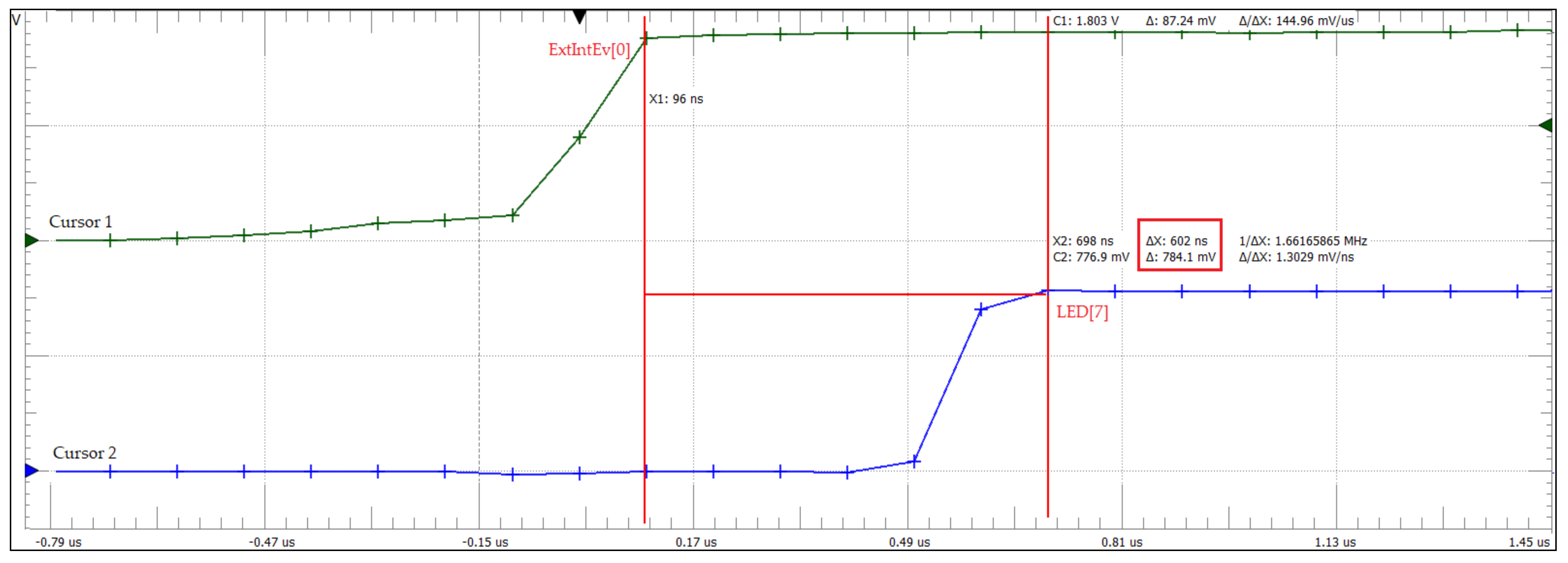
Figure 9 illustrates the jitter for verifying real-time scheduler performance implemented at the COP2-MIPS32-level. In this test, an Analog Discovery 2 oscilloscope by Digilent (Henley Ct. Suite 3, Pullman, WA, USA) was used for measuring the jitter of the preemptive scheduler in handling external asynchronous interrupts generated from the Virtex-7 kit. The address of the LED [
7] peripheral device is mapped in the address space of the data memory, and the state of this device is switched by extracting, decoding and executing the 0xadcc0000 MIPS sw instruction. Following the performed practical measurements, a response time of only 602 ns was obtained. To test the total response time and the jitter introduced by the scheduler, a system composed of 4 tasks was considered, with task 1 running on sCPU1 that would release a mutex to the task with the highest priority running on sCPU0 (sCPU2 and sCPU3 threat time-related events).
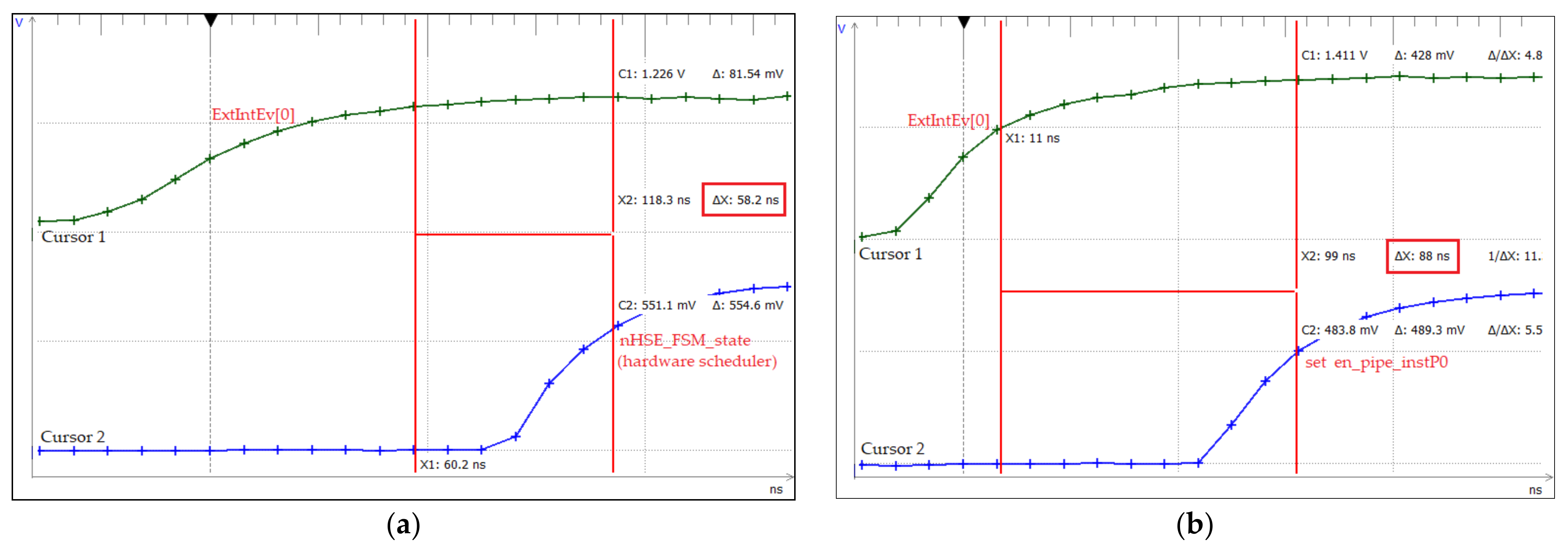
Figure 10 shows the tests performed to measure the kernel latency in the case of an event assigned to sCPU0, which is the highest priority event according to crEPRi (the register for prioritizing events at the sCPUi level, corresponding to crEVi).
Figure 10a illustrates the test performed for the practical measurement of the kernel latency corresponding to the nHSE scheduler (58.2 ns), i.e., the change in the output of the FSM states that generate the next transition through the nHSE_FSM_state[7:0] signals (time moment T2 from
Figure 6). Thus, tests were run to confirm that the hardware scheduler has a jitter of 1 clock cycle plus the time needed to trigger the IntEvi event (signal ExtIntEv[0] external interrupt), but any of the events specified in
Figure 3 can be triggered. In addition,
Figure 10b shows the oscilloscope capture for measuring the time of the thread context switch in 1 clock cycle, where the second cursor measures the transition of the signal nHSE_Task_Select (
Figure 6). The practical implementation of HW_RTOS_nMPRA in the FPGA validates the simulation presented in
Figure 6, so the kernel latency for handling an IntEvi-type event is only 88 ns (the trigger time of the external signal ExtIntEv[0] plus the 2 clock cycles needed for the hardware scheduler and the thread context switch).


