Article

A Parametric EIT System Spice Simulation with Phantom Equivalent Circuits

by
Christos Dimas
*,
Nikolaos Uzunoglu
and
Paul Peter Sotiriadis
*
Department of Electrical and Computer Engineering, National Technical University of Athens, 15780 Athens, Greece
*
Authors to whom correspondence should be addressed.
Technologies 2020, 8(1), 13; https://doi.org/10.3390/technologies8010013
Submission received: 2 December 2019 / Revised: 21 January 2020 / Accepted: 28 January 2020 / Published: 1 February 2020
(This article belongs to the Special Issue MOCAST 2019: Modern Circuits and Systems Technologies on Electronics)

Abstract

:
In this paper a number of LT Spice simulations have been carried out on an Electrical Impedance Tomography (EIT) system, which includes the whole analog and digital circuitry as well as the subject to be examined (phantom model). The aim of this study is to show how the analog and digital parts, the electrodes and the subject’s physical properties may impact the measurements and the quality of the reconstructed image. This could provide a useful tool for designing an EIT system. Special attention has been given to the current source’s output impedance and swing, to the noise produced by the circuits and to the Analog to Digital Converters (ADCs) resolution and sampling rate. Furthermore, some 3D phantom subjects have been modeled and simulated as equivalent circuits, merged with the EIT simulated hardware, in order to observe how changes on their properties interact with the whole circuitry and affect the final result. Observations show that mirrored current sources with z o u t > 350 k Ω and sufficiently high ADC acquisition sampling rate ( f s a m p l e 16 f i n ) can result to accurate impedance measurements and therefore quality image reconstruction within a frequency span of at least 10 to 100 kHz. Moreover, possible hardware failures (electrode disconnections and imbalanced contact impedances) can be detected with a simple examination of the first extracted image and measurement set, so that by direct modification of the reconstruction process, a corrected result can be obtained.

1. Introduction

Electrical Impedance Tomography (EIT) is a low-cost, safe and fast imaging technique which reconstructs the conductivity distribution of an examined object encircled by a cluster of electrodes, by injecting a low frequency current. Even though EIT is mainly used for medical purposes, its applications are extended to geophysical research and non-destructive evaluation.
Although this method is characterized by critically-low spatial resolution, especially near the center of the examined volume where the field sensitivity is decreased, its temporal resolution can reach exceptional levels, making EIT a great solution for real-time and time variant applications [1,2]. In addition, in the case of medical applications where conventional imaging methods such as CT, MRI and ultrasound cannot be used frequently and repeatedly on a patient (due to radiation, high cost, non-portability etc), EIT is a possible low cost alternative; EIT can serve as a complementary diagnostic and monitoring tool between two examinations from the previous methods.
Many EIT hardware systems with specific clinical applications have been developed over the last 3 decades, such as the Sheffield MK (v1 1987, v3.5 2001) [3], the Dartmouth breast imaging system (1998, 2001, 2008) [4,5,6], the ACT 3 and 4 EIT system (1994, 2005) [7,8], the Swisstom active electrode system (2012), the KHU Mark 2.5 system (2014) [9] and the ACE1 pulmonary real-time imaging system(2019) [1]. Over the years, many design and configuration improvements have taken place, targeted to the acquired medical images’ quality.
The image reconstruction problem of EIT is typically ill-posed and ill-conditioned, which means that even relatively low noise levels at the measurements could lead to significant reconstruction artifacts [10,11]. Therefore, apart from the essential mathematical modelling of the problem, the measured data need to be as accurate as possible with the minimum noise level. Intrinsic electrical bio-signals and unwanted motion of the electrodes (e.g., breathing or heartbeat) introduce noise in addition to noise due to electronic hardware [1,12]. Many of these cannot be easily predicted during the hardware design process. This creates the necessity for proper simulation before proceeding to the system design. Although many tools have been used for either the simulation of the tissue’s behavior in time and frequency (MATLAB-EIDORS tool, COMSOL, ANSYS, etc), of the contact impedance’s impact [13]; or the simulation of the hardware (SPICE for the current source behavior [14,15]), there is no complete effort to merge hardware (digital and analog), software and the subject’s properties on a single simulation core.
A preliminary parametric study has been presented in [11] where a whole EIT system circuitry has been simulated in LT Spice, including some 2D phantom equivalent circuits. It has been observed how possible problems such as increased signal noise and large contact impedance variation or more critical issues (electrode disconnections, short-circuits) contribute to imaging errors.
This work extends [11] in the following directions: A) It considers a more detailed model of the current source by including its output impedance, z o u t , depending on frequency f i n . Typically z o u t decreases in magnitude with f i n diverting from the ideal model, B) Digital to Analog Converter’s (DAC) quantization noise is included in the analysis, C) Proper analog filtering for antializing is included in the analysis, D) In addition to 2D, 3D Finite Element structures are developed in MATLAB and are imported into LT Spice as N-port equivalent circuits (N is the number of electrodes used.) to better simulate the EM field effects, and finally, E) The data acquisition system, including both the analog (filters, instrumentation amplifiers, voltage shifting in LT Spice) and digital (Analog to Digital Converter (ADC), data processing, image reconstruction in MATLAB) parts has been simulated. In addition, the transient effects, current injection and voltage acquisition channels switching times as well as the ADC noise, setting times and sampling rates have been taken into consideration [16].
A parametric study has been performed, modifying properties of the Voltage Controlled Current Source (VCCS), the electrodes, the structure (measuring subject) and the acquisition system within a frequency range of [10,100] kHz, in an effort to optimize the performance of an EIT system. Although there is difficulty in specifying hardware parameters in such complex systems, the presented simulations can be effective tools for system spec-determination and preliminary design; something that requires increased attention in EIT, since ostensibly small deviations or issues could lead to failure in the image reconstruction.
The paper is organized as follows: In Section 2 the EIT mathematical model along with the forward and inverse problems are briefly described. In Section 3, the simulated hardware in LT Spice is presented, highlighting the signal generation, the current source part, the subject equivalent circuit and the data acquisition process. In Section 4, EIT simulations are performed for selected VCCS topologies, frequencies, 3D tank phantoms, ADC sampling rates and resolutions, and the corresponding results are presented. The results are compared and discussed in Section 5. In the final section, conclusions are drawn.

2. The EIT Forward and Inverse Problem

The EIT electromagnetic problem is mathematically formulated by a current field diffused into a two- or three-dimensional volume Ω R d , d { 2 , 3 } which implies a Poisson differential equation [10,17]. The Complete Electrode Model (CEM) is the most popular EIT formulation. It takes into consideration the modelled electrode dimensions and is described by the following equations: [10,17]
· ( σ ( r ) u ( r ) ) = 0 , r Ω
u ( r ) + z l σ ( r ) u ( r ) n = U l , r e l , l = 1 , . . . , N
e l σ ( r ) u ( r ) n d S = I l , l = 1 , . . . , N
σ ( r ) u ( r ) n = 0 , r Ω l = 1 L e l
where u ( r ) is the voltage potential, N the number of the electrodes used, σ ( r ) is the relative distributed conductivity and z l the -th electrode’s contact impedance.

2.1. Forward Problem

The EIT forward problem assumes a known conductivity distribution σ in Ω and solves for the nodal (or element) voltage potentials. This is usually done using the Finite Element Method (FEM) after converting (1) to its weak form for every element and embedding boundary conditions (2)–(4). After assembling the local element matrices, the problem results in a sparse (3-diagonal) linear system equation that can be solved with the Cholesky or the Conjugate Gradient algorithms [10].

2.2. Inverse Problem

The inverse problem refers to deriving σ ( r ) for a known voltage potential distribution u ( r ) and the voltage measurements on the electrodes U. Contrary to the forward problem, this one is severely ill-conditioned and requires special regularization in order to derive a stable solution. The solution given by the generalized Tikhonov regularization is [10,17]
σ ( r ) = σ r e f ( r ) + ( M T W M + λ 2 Q ) - 1 M T W δ U
where σ r e f ( r ) is a reference conductivity distribution, W is a weighting matrix indicating each measurement’s impact, M is the Jacobian matrix representing the sensitivity of each measurement to a conductivity change. In addition, Q is a prior filter matrix, λ is the regularization hyperparameter and δ U is the difference between measurements acquired for σ r e f ( r ) and σ ( r ) respectively [10,17,18]. Although this is a direct one-step solution, many iterative approaches have also been developed, e.g., Gauss–Newton algorithm. However, in terms of this study, the NOSER prior one-step algorithm [10] is used with Q = d i a g ( M T M ) , since parametric hardware tests are performed and NOSER is a simple, easy to implement reconstruction algorithm in order to check the effectiveness of an EIT hardware. Of course, similar comparison results with small variations are expected if the reconstruction is performed with any other one step inverse algorithm (0th order Tihkonov, Laplace, Gaussian High Pass Filter, D-Bar) or an iterational one (Gauss–Newton). The size of variations between the hardware simulations depends on the inverse algorithm’s noise robustness, therefore, in order to get clearer comparisons we did not select a high performance reconstruction algorithm.

3. EIT Hardware

It has been shown that the tetrapolar measurement technique is the most suitable for EIT especially in bio-impedance instrumentation [17]. To implement is, a sinusoidal (or bi-frequency) current source (up to 1 mA, 10 kHz–100 kHz) is needed, followed by a multiplexing array to drive and sink the current from an electrode pair and take differential measurements from all electrode pairs. More details about the complete system architecture can be found in [11].
Here, we focus on (a) the current source topology and its properties, and, the their impact on the measurements and image reconstruction quality, on (b) the development of an electrical equivalent model of a typical phantom used for evaluating the performance of EIT image reconstruction algorithms, and on (c) the impact of the data converters properties on the image reconstruction quality.

3.1. The Current Source

The current source circuitry part described here includes the (voltage) signal generation, the filtering stage and the Voltage Controlled Current Source (VCCS).

3.1.1. Signal Generation

For signal generation, a Direct Digital Synthesis (DDS) block is usually a suitable solution. This includes a DAC driven by a sinusoidal or more complex waveform, typically stored in a Look-Up-Table (LUT). The analog output signal-to-noise ratio (SNR), considering only the quantization noise, of an L-bit DAC is [11]
S N R ( dB ) = ( 6.02 L + 1.72 ) dB + 10 log 10 O S R
where O S R is the oversampling ratio. In this study, we simulated a 16 bit DAC (14 bit ENOB) with a sampling frequency of 16 times the desired signal frequency ( f i n ) , i.e., with O S R = 8 . Data were written on a text file (.txt) which was used as a PWL LT Spice voltage source.
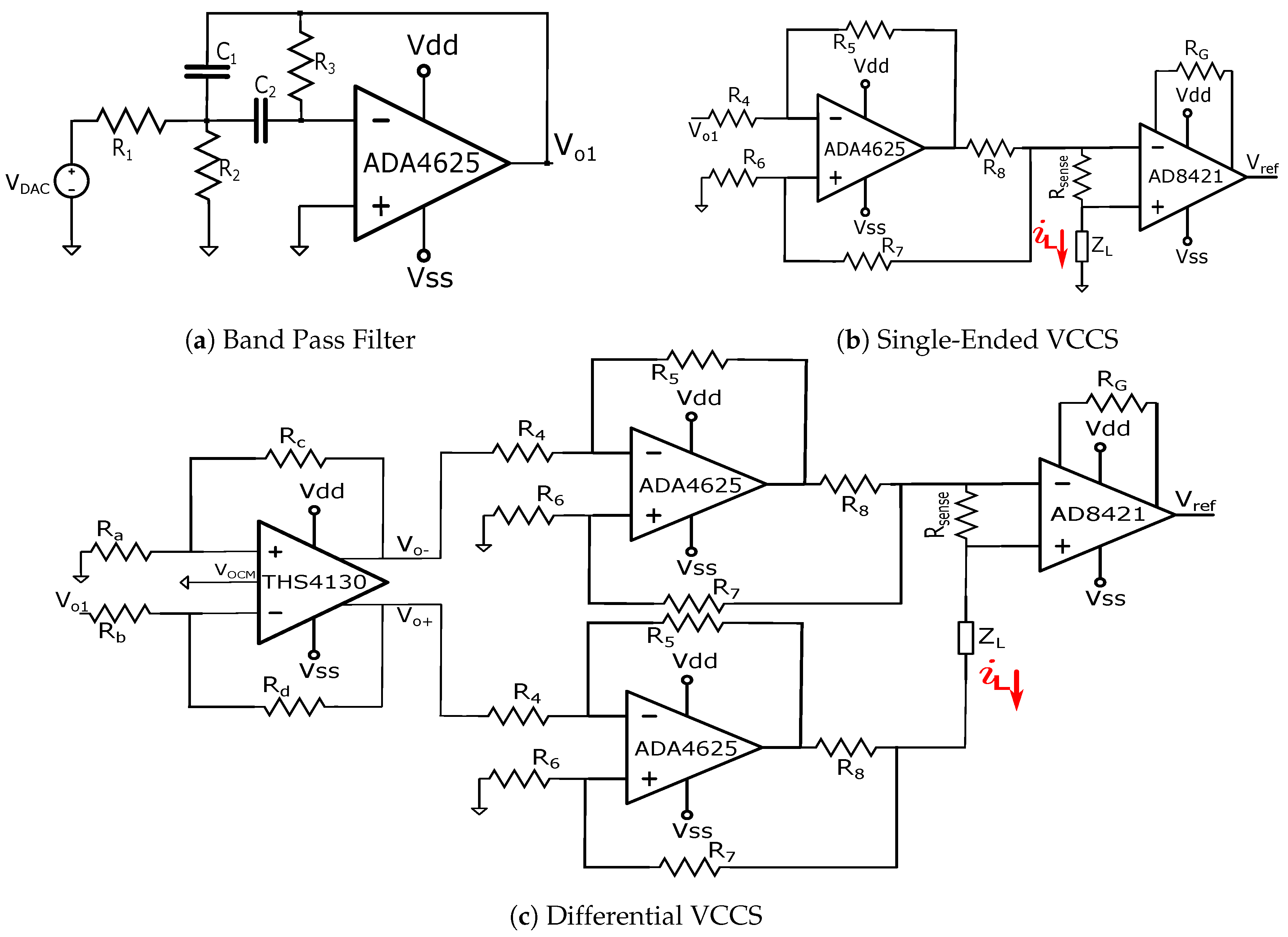
The DAC’s output is filtered by an analog low-pass or band-pass filter. In our case, we use a 2nd order multiple feedback active band-pass filter with a central frequency of f i n and quality factor of Q = 5 [19]. The filter (shown in Figure 1a) was simulated using the ADA4625 Opamp (analog devices).

3.1.2. Voltage-to-Current Conversion

The design of an appropriate VCCS is one of the most challenging parts in an EIT system design, since the specifications must satisfy high output impedance z o u t , Common Mode Rejection Ratio (CMRR) and sufficient current amplitude (low enough for the patients’ safety and high enough to avoid notable noise rates) for as high frequency range as possible. In this study the topologies simulated are based on the modified Howland current source, described in [14,20,21]. Specifically, two main approaches have been tested: (a) the grounded load and (b) the mirrored modified Howland VCCS [20]. Their topologies are shown in Figure 1b,c correspondingly. The mirrored VCCS is driven from a THS4130 fully differential amplifier, which follows the analog filter and offers low noise levels (1.3 nV/ H z ) and an acceptable slew rate (51 V/ μ s). The Common Mode Voltage V C M was connected to ground. All ICs were supplied with +/− 15 Volts. In addition, since the mirrored VCCS needs to be symmetric, the corresponding resistors are of the same value ( R 4 - R 8 in Figure 1c). In order to be able to measure the input current to the load, an instrumentation amplifier (AD8421) stage has been added with a fixed sense resistor R s e n s e between its inputs and a configurable gain R G resistor [22].
The output impedance z o u t of Howland current sources depends on the balance of the resistors R 4 - R 8 which is extremely sensitive. Therefore the resistors above need to be characterized by very low tolerance ( δ R / R 1 % ). Furthermore, they are affected by the open loop gain of the Opamp (A), which is exposed to factors such as frequency and temperature. Those dependencies can be expressed at an approximate way by the following equations for the grounded load case: [20]
Z o u t , m i n = R 8 R 6 δ R 4
Z o u t = R 4 R 8 ( R 7 + R 6 ) A + R 8 ( R 7 + R 6 ) ( R 4 + R 5 ) [ R 4 ( R 7 + R 8 ) - R 5 R 6 ] A + ( R 4 + R 5 ) ( R 6 + R 7 + R 8 )
From the equations above it is concluded that small perturbations of the resistor-coefficients not only could result in a much smaller than expected z o u t but also to unstable oscillations (since the Opamp already has a positive feedback) [20,23]. Another important issue occurs from the parasitic impedances while f i n increases, that lead to a severely decreased z o u t and intense changes of the phase shift. The phase shift can be easily estimated from simulation and circuit testing and be added as a parameter when necessary in the acquisition part. Nevertheless, | z o u t | can hardly be kept above 200 k Ω for f i n 100 kHz, which leads to a large percentage of current steer before the load. Simulations performed show that increasing R 8 , optimises the condition for the larger frequencies at the cost of current amplitude reduction that results in lower measurement SNR due to white noise and lower resolution.
The mirrored Howland VCCS improves on these issues, since it has larger z o u t which arises from the sum of the two single ended circuits z o u t [20]. The current amplitude is also larger and can be adjusted from the THS4310’s gain (setting R c and R d to proper values). In Figure 2, simulations show the z o u t and the current amplitudes for the two topologies, using the ADA4625 and OPAx210 Opamps. Additionally, a transient simulation that includes the DAC, filter and VCCS output for parametric R 8 resistor is displayed. A 300 Ω resistor in series with a 0.1 uF capacitor were used as load. The resistor values and tolerances selected are shown in Table 1.
From the simulation displayed, it is shown that with a mirrored VCCS z o u t can reach 400 k Ω using the ADA4625 Opamp and even 700 k Ω using the OPAx210 Opamp with R 8 4 k Ω . The load current amplitudes are also kept at levels around 500 uA which are appropriate levels. In reality, the corresponding real z o u t values have some randomness and may differ, however those simulations demonstrate the order of their magnitude [20], which is an important factor to be taken into consideration during EIT designing.
In the literature, the first EIT systems developed in the late 1980s–early 1990s used single-ended current sources [3,24]. Due to the degradation caused by the relatively low output impedance, combined with parasitic capacitances, calibration stages (negative impedances at first and Generalized Impedance Converters (GICs) later in the mid-2000 s) were used for the cancellation of stray capacitances and maximization of the | z o u t | [4,5,6,7,8,9,25]. This approach assisted on achieving superior output impedance values (up to 2 M Ω at 100 kHz [9]), allowing proper operation at frequencies up to 1 MHz [4,5,6]. Small modifications have also been performed on the Howland VCCSs in order to prevent oscillations (capacitors parallel to the negative feedback [9]).Some other implementations included the mirrored VCCS [1,26] or other approaches (Bragos) [27,28]. In [28] the current imbalance between source and sink is addressed by measuring the current and adjusting its amplitude. Most of those systems are characterized by z o u t from a hundred to several hundreds of k Ω at [10,100] kHz.
However, negative impedance circuits might suffer instability due to overcompensation of stray capacitance, [29]. Furthermore GICs need continuous calibration and are incapable of performing over large frequency spans simultaneously (limited bandwidth) [9]. Thus, often multiple GICs are essential, where each one covers a small specific frequency range. On the other hand, differential VCCSs need precise resistor matching with very low tolerances and cause higher white noise levels due to the large number (and values) of resistors used [26]. In each case, the designer has to estimate the pros and cons of his choice, taking into consideration the application targeted and its standards.

3.2. Equivalent Circuits

The subject circuit equivalent can be formed by transforming the FEM mesh along with its element admittance values to a N-electrode port RLC circuit. Nevertheless, apart from the examined volume’s properties, it is important to include the effect of the electrode properties which contain: (a) their displacement and area, which affects the order of the measured impedance and (b) their contact impedances that need to be balanced and depend on the electrode material. The CEM described in Section 2, assists to this direction, since it considers about the electrode geometry and z c o n t a c t . However, in terms of this study, we included only the displacement in the FEM mesh; whereas the electrode equivalent circuit was simulated separately at LT Spice before the N-port inputs, in order to observe each individual component’s effect at the measurements, and not just the z c o n t a c t value’s one.

3.2.1. Electrode Equivalent

Briefly, the simplest electrode equivalent circuit model consists of a parallel combination of a resistor R c t and an interface capacitance C c p (actually a constant phase component), in series with a solution resistor R s which indicates the impedance between electrode and subject’s surface (skin) [11,30]. More detailed electrode equivalent models can be found in [30,31,32]. In this particular study, simulations are reduced to 3D salted water tanks, therefore very small R s values have been chosen (<2 Ω ). In addition, crosstalk capacitances of less than 100 pF have also been included (see Figure 3), representing the electrode lead wire capacitive effects as well as the multiplexer’s stray capacitances. The parasitic effects caused by the electrodes, switches and lead wires can be greatly reduced with the usage of active electrodes [1,2,33]. However, an active electrode system implementation can highly increase the total hardware cost.

3.2.2. Subject Equivalent

Let as consider the simulated FEM system equation, which gives the nodal voltages U i , for i { 1 , . . . , n } nodes:
A m + A z A v A v * A D U V l = 0 I d
where A m R n X n has resulted from the local element matrices assembling, A z R n X n and A v R n X N from the boundary conditions (2)–(4) and A d R N X N refers only to the nodes where the measurements are taken [10]. V l N indicate the measurements and I d the current injected. Let us write A k = A m + A z . Then, by expanding the system (9):
A k U + A v V l = 0
A v * U + A d V l = I d
Solving for the nodal potentials and the measurements we get:
U = - A k - 1 A v V l
V l = A d - 1 I d + A d - 1 A v * A k - 1 A v V l
The last equation is written:
( I N - A d - 1 A v * A k - 1 A v ) V l = A d - 1 I d
Therefore
( A d - A v * A k - 1 A v ) V l = I d
F ( σ ) = A d - A v * A k - 1 A v corresponds to the sparse and almost symmetric conductivity matrix considering each measuring point as a node [34]. Thus, the result is a N-port system, where each impedance between two nodes i and j is computed as: Z i j = - 1 / F ( σ ) i j [35].

3.3. Data Acquisition

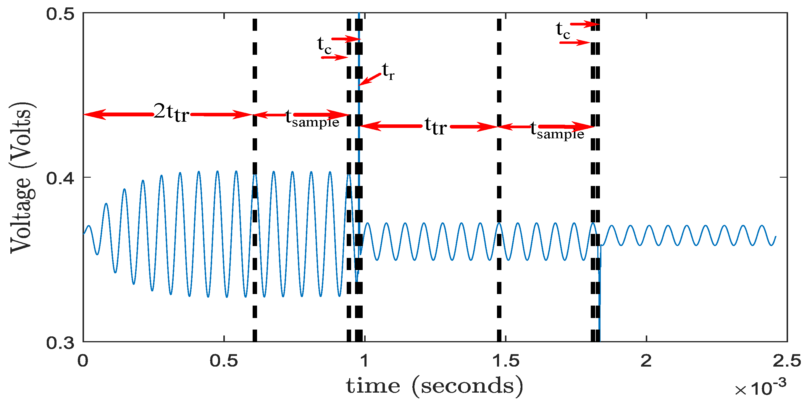
In order to get an EIT image frame, when using a current skip-i pattern and a voltage skip-j pattern [36], N ( N - 3 ) measurements are conventionally needed if i = j or N ( N - 4 ) else. Each measurement is traditionally taken for a particular set up of current source, sink and voltage measuring electrodes. Between each couple of measurements, a transient effect takes place due to the analog multiplexer switching, the network’s parasitic behavior and subject’s admittance behavior. After those effects ceased the output signal comes to Steady-State (SS) and an integer number of periods has to be properly sampled by an ADC (as shown in Figure 4).
Spice EIT transient simulation is set as follows: the multiplexers’ digital inputs are defined by PWL sources. The pulse rising times t r have also been considered, according to the multiplexer’s specifications (ADG426). After each multiplexer’s change, a t t r time is inserted as the needed time to reach the SS. During t t r the ADC can be initialized or send the previous samples to a DSP/MCU and set to the proper state to sample. t t r usually lasts about 200–300 u s and can be extended if the essential configurations have not already finished.
When t t r ends, the corresponding T s t a r t time point is written at a .txt file by MATLAB. Then follows the t s a m p l e (conversion time) which is the time ADC needs to sample the output signal when at SS. It is recommended to be an integer number k (5 to 10) of the signal’s period T i n = 1 / f i n . After the sampling is finished, T s t o p time point is written to the text file. t c time (in the order of ns) is then needed for the multiplexers to get the order and change their state. For each measurement we have T s t o p - T s t a r t = t s a m p l e and the total time needed for the acquisition of a single measurement is:
t m e a s = t r + t t r + t s a m p l e + t c
If a particular measurement is taken after a current source position change this duration is increased as follows:
t m e a s = 2 t r + 2 t t r + t s a m p l e + t c
The total time when using pairwise injection protocol (adjacent/ skip-0) is:
t f r a m e = N 2 ( t r + t t r + k T i n + t c ) - N ( 2 t r + 2 t t r + 3 k T i n + 3 t c )
t f r a m e obviously depends on the electrode number N, the input signal frequency f i n and the ability of the ADC to send the samples quickly to the MCU. It is assumed that any post-acquisition signal processing is performed after the acquisition process has been completed.
The output voltage signal V o u t is sent to MATLAB after the SPICE transient simulation has ended. Then sampling is performed between each T s t a r t and T s t o p time point, using a cost minimization function between the desired and the actual sampling times, since Spice simulators do not use constant time steps [37]. Only the first 14 Most Significant Bits (MSB) out of 16 bits of the simulated ADC are used (ENOB), since the two Least Significant Bits (LSBs) are considered as noisy and distorted.
For each measuring window m { 1 , . . . , N ( N - 3 ) } an amplitude is obtained by the difference of the medians between the five maximum and the five minimum voltage values from the ADC sampled voltage values V o , n e w . The amplitude values are stored in the A m p l i t u d e s ( m ) vector, which is usually normalized, by setting its maximum value to 1. A m p l i t u d e s ( m ) vector is then utilized as raw data for the image reconstruction. In order to get a reliable result from the process described above, it is strongly recommended that f s < < f s p i c e _ m i n , where f s p i c e _ m i n is the minimum Spice sampling frequency, which is defined as the inverse of the maximum Spice time step.

4. EIT Simulations and Results

4.1. Structures

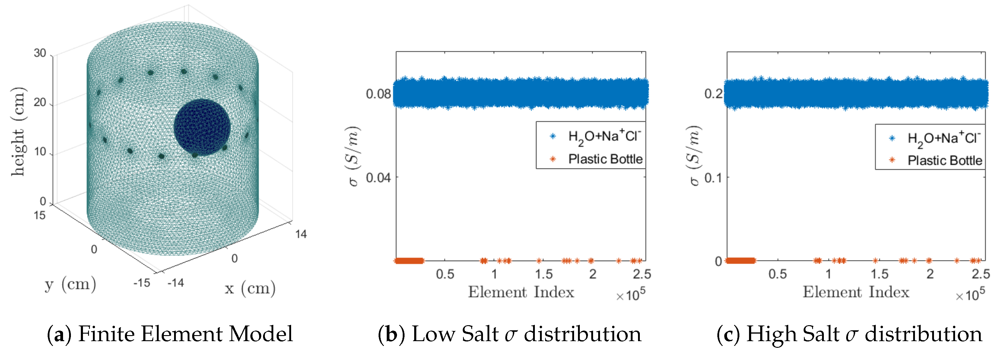
In this work, a 3D cylindrical tank FEM model attached around with 16 electrodes has been used as an input for the subject equivalent circuit. Each image frame occurs from the measurement difference between two cases (differential EIT, used for either time differential (td-EIT) and frequency differential (fd-EIT)): (a) the reference, which in this case is taken on an almost homogeneous water-salt tank and (b) the inhomogeneous or final, where a plastic -non conductive- object has been inserted in the tank. Furthermore, the FEM model has the following characteristics: height of h = 30 cm, radius R = 15 cm and circular electrodes of r e l = 0.5 cm radius attached at z = h e l = 20 cm. The model contains a total of 48,080 nodes and 254,475 elements and was constructed in MATLAB with the NETGEN mesh tool. The plastic spherical object’s centre was put at C s p h e r e = (6.5, 0, 15) cm and its radius was selected to be r s p h e r e = 5 cm.
The conductivity value set to each element in the sphere was σ = 10 - 4 S/m. For the water with sodium chloride conductivity 2 cases have been introduced: (a) a low salt concentration where each out-of-sphere element has a σ with follows a normal distribution of μ = 0.08 and v a r = 16 × 10 - 4 . (b) A moderate salt concentration where the normal distribution of σ has μ = 0.2 and v a r = 4 × 10 - 3 . The values were chosen based on the fact that drinking water has σ < 0.05 S/m and sodium-chloride natural and sea water conductivity measurements under constant temperature (approx. 25 C) have a variability range of 2–5% [38,39,40]. Figure 5b,c show the conductivity defined at each element for both cases, when plastic object is inserted.

4.2. Test Cases

At all the test cases (T1–T4), the adjacent skip-0 current pattern [36] was used, along with the NOSER one-step reconstruction algorithm, with a heuristically selected hyperparameter λ = 0.3 . For the inverse model (where the image reconstruction is performed), a circular point electrode model which includes 1024 equal sized triangular elements was selected. The input signal frequency was f i n = 15 kHz and f i n = 100 kHz. The DAC was simulated with L = 16 bits (ENOB 14) and f s = 16 f i n .
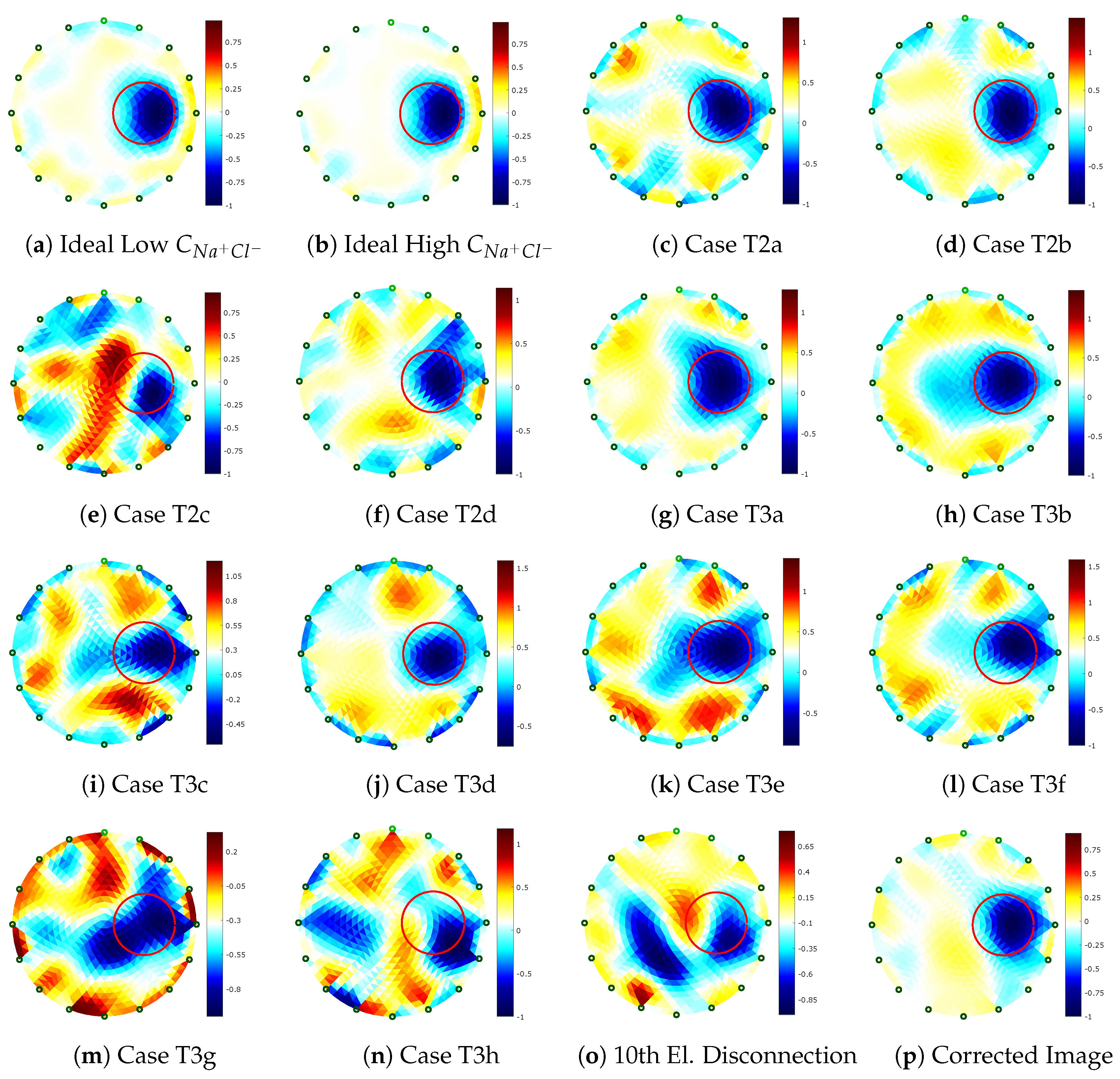
FEM Simulation (T1a-b): Firstly, an EM measurement simulation was performed with the EIDORS library tool in MATLAB [41], by directly solving the forward model of the two structures described before. The simulated measurements were used as inputs to the inverse problem. This test shows the imaging algorithm’s performance and demonstrates the measurements behaviour assuming optimal hardware functionality. Therefore, its results (T1a for low N a + C l - concentration and T1b for moderate N a + C l - concentration), shown in Figure 6a,b, are used as a reference for the following test cases.
Single-Ended Current Source (T2a–d): A hardware simulation test was performed for the 2 N a + C l - concentrations at f i n = 15 kHz using the grounded load modified Howland VCCs described in Section 3.1.2. For the acquisition the ADC was assumed to operate at L = 16 bits, V A D C = 3.3 V with f s = 240 ksps and f s = 1 Msps. The corresponding images are displayed in Figure 6c–f.
Mirrored Current Source (T3a-h): These simulations were also executed for the 2 structures described in Section 4.1, for f i n = 15 kHz (T3a-d) with the same ADC properties as in (T2) and for f i n = 100 kHz (T3e–h), with ADC simulated at L = 16 bits with f s = 1 Msps and f s = 2 Msps. Although the N a + C l - properties do not significantly change in the frequency range of [10,100] kHz (something that does not apply to soft human tissues), the currents source’s z o u t is significantly reduced as shown in Section 3. Therefore, more errors are expected to be introduced at the measurements. The results are shown in Figure 6g–n.
Disconnected electrode, imbalanced z c o n t a c t s (T4a-b): A final Spice simulation was performed for the case of disconnection at the 10th electrode ( R s was set to 1.5 M Ω ) and increased solution resistances at 3rd and 5th electrodes (about 10 times the other electrodes’ R s ). f i n was set to 15 kHz, the mirrored VCCS topology was acted and the 16 bit simulated ADC was sampling at f s = 240 ksps.
At each testcase T2–T4, a - 55 dB SNR white noise was directly added to Spice output signals before the ADC acquisition.

4.3. Error Estimation

Since the purpose is to estimate the error introduced exclusively from EIT hardware, the measurements simulated and the images produced for the T1 test case are utilized as the desired values. At this point it is important to note that in order to perform a valid comparison, all cases have to be treated with the same reconstruction algorithm parameters, defined in Section 4.2. It is also necessary to have all values normalized. The Mean Absolute Percentage Error (MAPE) is defined as:
M A P E M e a s = 1 M i = 1 M V d i - V e i V d i · 100 %
where V d is the measurement vector from the direct FEM simulation (case T1) and V e the measurements from the hardware simulations after the acquisition process (cases T2–T4). In addition, M is the total number of measurement values per frame (i.e., M = 208 ).
The corresponding M A P E for the reconstructed images is defined by the following equation:
M A P E I m a g = 1 K i = 1 K σ d i - σ e i σ d i · 100 %
where σ d is the normalized σ (for absolute imaging) or difference σ vector (for difference imaging) resulted from the FEM simulated measurements (case T1) and σ e is the corresponding vector resulted from the hardware parametric simulations (cases T2–T4). K is the number of elements used in the inverse model (i.e., K = 1024 ). Both MAPE errors are shown in Table 2.
We also introduce the Reciprocity Error ( R E ) for each homogeneous measurement set:
R E = u ( i , j ) I ( m , n ) - u ( m , n ) I ( i , j ) u ( i , j ) I ( m , n ) · 100 %
where u ( i , j ) I ( m , n ) is the voltage difference between electrodes i and j when current is injected from electrodes m and n [9,28].

4.4. Image Correction

In case the measurements are corrupted due to issues that are correlated with bad electrode contacts, disconnections or ever short-circuited lead wires, it is possible to correct the output image, provided there is knowledge of the erroneous electrodes. Then, the weight matrix W (see Section 2) can be properly corrected so that the inverse problem will not take into account any measurement correlated with those electrodes [42,43].

4.5. Results

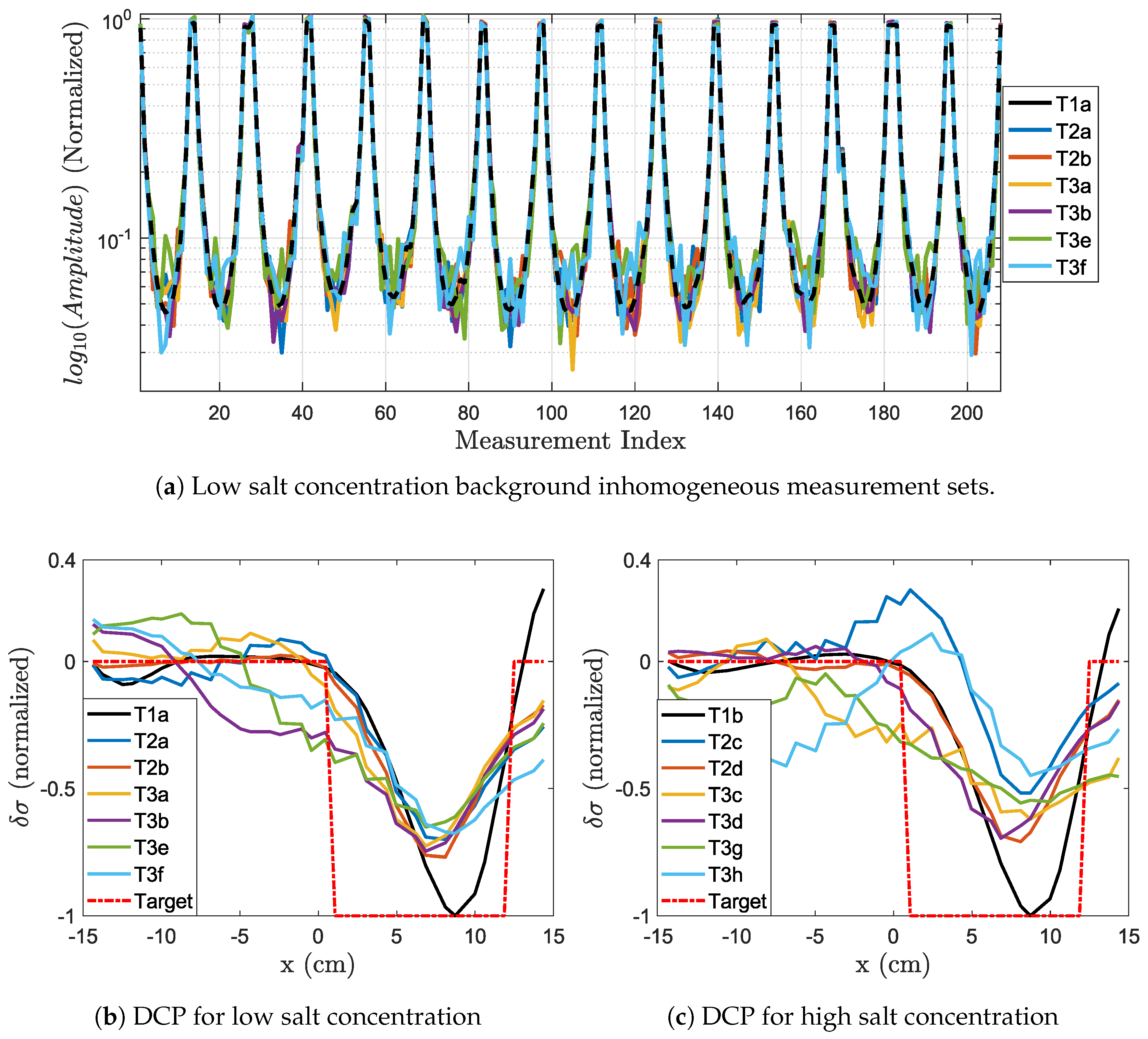
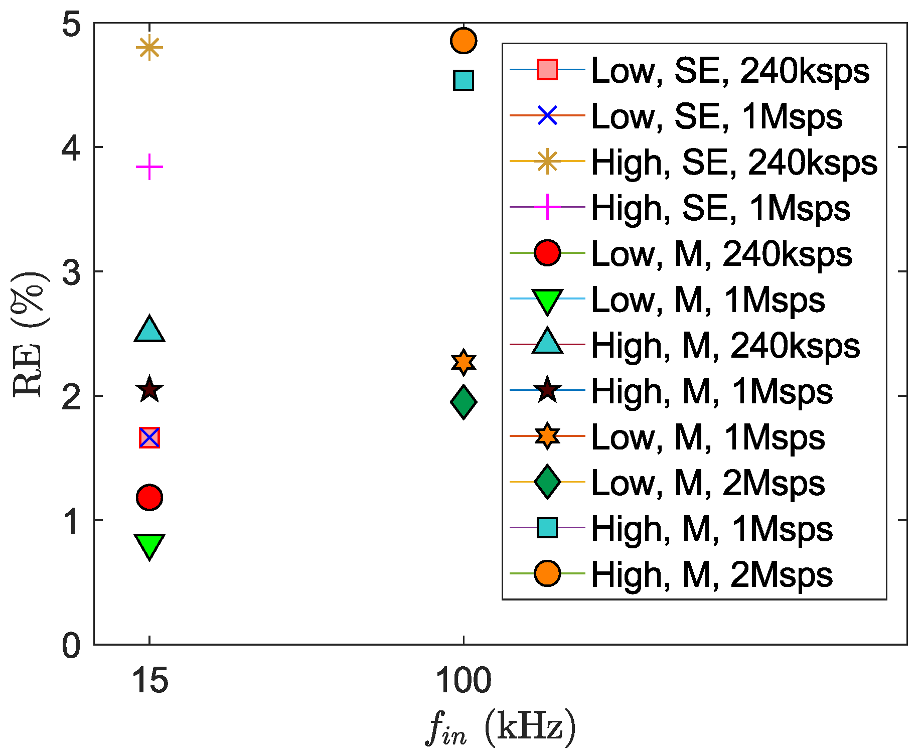
The (normalized) difference conductivity distributions δ σ estimated for each particular case described in the previous section are displayed in Figure 6. The structures used for the simulations were described in Section 4.1. For the filter and the VCCS parts of the hardware the ADA4625 Opamp was finally selected, since the utilization of numerous OPAx210 Opamp models simultaneously with the whole circuitry caused instability to Spice simulations. Due to each testcase’s various parameters, each of them is indicated at Table 2 for clarity, along with the corresponding M A P E errors estimations. In Figure 7 the (normalized) inhomogeneous amplitude measurements for the 1st structure cases (low salt concentration) are also displayed, along with the Diametric Conductivity Plot (DCP) for both N a + C l - concentrations [44]. Figure 8 displays the reciprocity percentage errors estimated for each testcase T2a–d and T3a–h. All results are discussed in the next section.

5. Discussion

From the simulations described, it is observed that both the reconstructed image artifacts and the measurement and imaging errors along with R E are potentially decreased in cases when high- z o u t VCCS and high- f s ADC are combined. Specifically, the minimum errors are obtained in test case T3b (Figure 6h shows the object completely in the red circle), where we used a mirrored Modified Howland VCCS with a z o u t estimated just over than 1 M Ω at f i n = 15 kHz according to the results in Section 3. Furthermore, the f s is 1 MSps which is over 64 times the input signal frequency f i n . The corresponding R E was estimated at 0.81 % (pointed with a green triangle in Figure 8). That satisfies the EIT literature hardware standards ( R E < 2 % for typical performance, R E < 1 % for high performance) [5,9,28].
When the input signal frequency ( f i n ) is increased to 100 kHz and measurements are taken at the same structure, the mirrored VCCS z o u t is decreased to 400 k Ω , causing current distortion. Moreover, the sampling rates of 1 MSps and 2 MSps cannot be characterized as oversampling when f i n = 100 kHz. This results in larger measurement errors (case T3f in Figure 6l where the case of f i n = 100 kHz exhibits greater error than case T3b in Figure 6d where f i n = 15 kHz, while both tests use Mirrored VCCS; same happens with cases T3d and T3g). Overall, increasing the input frequency from 10 kHz to 100 kHz causes a measurement SNR reduction from 5 dB [6] to 20 dB [9] at implemented hardware EIT systems, resulting in a corresponding image quality reduction [9].
In addition, when increasing N a + C l - concentration in the water, the mean value and range of the background’s σ is increased (see Figure 5b,c). This results in lower impedance values between each electrode channel and thus very small measuring amplitudes. Even with a 54 dB-gain instrumentation amplifier (an AD8421 with R G = 20 Ω ), the measured amplitudes barely reach the value of 1 mV when the measure is performed far from the current injected electrodes. Taking into account the signal’s noise and the ADC’s capabilities, the raw voltage input to the reconstruction algorithm suffers from very low SNR. This has an obvious impact on the M A P E M e a s and M A P E I m a g values as shown in Table 2 and the imaging precision and quality as shown in Figure 6: Low C N a + C l - cases (T2a, T2b, T3a, T3b, T3e, T3f) have been reconstructed with greater success than the high C N a + C l - ones: (T2c, T2d, T3c, T3d, T3g, T3h); the results are independent of the hardware specifications used in the simulations. Since the measurement accuracy has been reduced, the R E has increased accordingly, reaching the unacceptable for typical EIT design levels of 4–5% (see the 4 highest values in Figure 8). However, in the literature R E is measured at homogeneous saline tanks of σ = 0.05 S/m to 0.1 S/m [5,9,28]; a value much lower than the current value of 0.2 S/m. Therefore, the low salt concentration R E levels are more representative for the hardware’s performance. It is also confirmed that higher measurement errors generally lead to higher imaging errors. However, this relation is not proportional; it is rather characterized by a non-linearity which is correlated to the inverse problem’s non-linear nature.
The Diametric Conductivity Plots (DCP, Figure 7b,c) show that most cases detect the decreased conductivity in the red circle area. However, the reconstruction algorithm is not able to properly centralize the minimum conductivity point of the target (which occurs at x = 6.5 cm), even at the EM simulation (test case T1). This can be explained by the 3D nature of our set-up; the target object is located some centimeters down from the electrode slice (z-layer). Therefore, the currents streamlines go through longer distance in the field until they come across the plastic object and change direction. This results in a deviation between the object’s detected position and the actual horizontal position. Moreover, artifacts occur for x < 0 cm, where the actual conductivity change δ σ is negligible. The δ σ in most cases follows the corresponding M A P E M e a s and M A P E I m a g , since (as referred earlier) larger deviations in measurements lead to further imaging artifacts. A hard exception occurs for the T3b case (Mirrored VCCS, low salt concentration, f i n = 15 kHz, f s = 1 MSps), where despite featuring the least erroneous measurements and the minimum M A P E I m a g , it has a modest DCP error. However, an observation of the corresponding image reconstruction (Figure 6h) shows that the total image artifacts are less intense than most other cases where f i n is larger and f s smaller. Besides, the red circle area identifies the low conductive blue one.
Examining the test case T4, it is shown (Figure 6o) that due to an electrode disconnection the reconstruction completely fails: the target object cannot even be distinguished. However, a-priori knowledge of the structure’s behavior (a non-conductive object is supposed to appear near the red circle), combined with careful examination of the image leads to the hypothesis that there is a major error near the electrodes 9–10. Properly modifying the measurement weight W matrix, we get a new measurement set, fully uncorrelated with electrode 10, which contains 156 measurements instead of the initial set of 208 measurements. The improvement in Figure 6p is significant, since the majority of artifacts has been erased. For case T4b, the M A P E m e a s was estimated using only the 156 valid measurements. Thus, the R E was not estimated for this test case.
In general, the design of an EIT hardware system is a process where numerous parameters have to be taken into consideration and the specifications are deeply depended on its application field. For instance, a real-time thoracic-imaging EIT system needs to be characterized by very high framing speed [1,33]; this requires higher current signal frequencies, in order to accelerate the acquisition pipeline described in Section 3. This leads to the necessity of designing a high- z o u t VCCS over a large frequency range; moreover, the designer must combine the high-perfomance VCCS with an ADC with high throughput rates. Another example is a brain-imaging EIT system, where lower frequencies are utilized; however, due to the skull’s very large impedance the z c o n t a c t dramatically increases and the current source should be capable of driving much higher impedances [28].
In all cases, the use of single-ended Howland current pumps without any negative impedance calibration or calibration via current amplitude measurement should be avoided. On the other hand, if the designer chooses a mirrored Howland architecture he must consider carefully the resistors matching and the amount of Johnson noise (trade-off between balance suceeded with high valued, low tolerance resistors and low noise achieved by low value resistors). Furthermore, the ADC sampling rates are strongly recommended to exceed the signal’s frequency over 10 times, a condition that has been adopted by most EIT systems [1,6,17,28,33]. Both factors (high z o u t , acquisition rates) have a significant impact on the measurements quality.
6. Conclusions

In this work we performed an extensive Spice simulation study for EIT system design, assisted by MATLAB. It was shown that EIT measurements and thus image reconstruction are very sensitive to hardware specifications such as the current source z o u t , the electrodes connectivity and the ADC configuration. All the system parts have to be designed at a proper way to get a balanced performance by minimizing artifacts due to the hardware issues and then deal with the inverse’s problem ill-conditioned nature. Some more parameters and parts have to be further examined in a future work, such as the electrode material, realistic tissue equivalents and IQ demodulation, in order to get a complete simulation setup, that can be used to select EIT design parameters.

Author Contributions

Investigation, C.D.; Writing–original draft, C.D. and P.P.S.; Writing–review and editing, C.D., N.U. and P.P.S. All authors have read and agreed to the published version of the manuscript.

Funding

This research is co-financed by Greece and the European Union (European Social Fund- ESF) through the Operational Programme “Human +Resources Development, Education and Lifelong Learning” in the context of the project “Strengthening Human Resources Research Potential via Doctorate Research” (MIS-5000432), implemented by the State Scholarships Foundation (IKY).

Conflicts of Interest

The authors declare no conflict of interest.

References

  1. Mellenthin, M.; Mueller, J.; de Camargo, E.D.; de Moura, F.S.; Santos, T.B.; Lima, R.G.; Hamilton, S.J.; Muller, P.; Alsaker, M. The ACE1 Electrical Impedance Tomography System for Thoracic Imaging. IEEE Trans. Instrum. Meas. 2019, 68, 3137–3150. [Google Scholar] [CrossRef]
  2. Gaggero, P.O. Miniaturization and Distinguishability Limits of Electrical Impedance Tomography for Biomedical Application. Ph.D. Thesis, University of Nechatel, Nechatel, Switzerland, 2011. [Google Scholar]
  3. Wilson, A.J.; Milnes, P; Waterworth, A. R.; Smallwood, R.H.; Brown, B.H. Mk3.5: A modular, multi-frequency successor to the Mk3a EIS/EIT system. Physiol. Meas. 2000, 22, 49–54. [Google Scholar] [CrossRef]
  4. Halter, R.J.; Hartov, A.; Paulsen, K.D. Design and implementation of a high frequency electrical impedance tomography system. Physiol. Meas. 2004, 25, 379–390. [Google Scholar] [CrossRef] [PubMed]
  5. Halter, R.J.; Hartov, A.; Paulsen, K.D. A broadband high frequency electrical impedance tomography system for breast imaging. IEEE Trans. Biomed. Eng. 2008, 55, 650–659. [Google Scholar] [CrossRef]
  6. Khan, S.; Manwaring, P.; Borsic, A.; Halter, R.J. FPGA Based Voltage and Current Dual Drive System for High Frame Rate Electrical Impedance Tomography. IEEE Trans. Med Imaging 2015, 34, 888–901. [Google Scholar] [CrossRef] [PubMed]
  7. Cook, R.D.; Saulnier, G.J.; Gisser, D.G.; Goble, J.C.; Newell, J.C.; Isaacson, D. ACT3: A high-speed, high-precision electrical impedance tomograph. IEEE Trans. Biomed. Eng. 1994, 41, 713–722. [Google Scholar] [CrossRef] [PubMed] [Green Version]
  8. Liu, N.; Saulnier, G.J.; Newell, J.C.; Isaacson, D.; Kao, T.-J. ACT4: A high-precision, multi-frequency electrical impedance tomograph. In Proceedings of the 6th Conference on Biomedical Applications of Electrical Impedance Tomography, London, UK, 22–24 June 2005. [Google Scholar]
  9. Wi, H.; Sohal, H.; McEwan, A.L.; Woo, E.J.; Oh, T.I. Multi-Frequency Electrical Impedance Tomography System With Automatic Self-Calibration for Long-Term Monitoring. IEEE Trans. Biomed. Circuits Syst. 2013, 8, 119–128. [Google Scholar]
  10. Polydorides, N. Image Reconstrucion Algorithms for Soft-Field Tomography. Ph.D. Thesis, University of Manchester Institute of Science and Technology, Manchester, UK, 2002. [Google Scholar]
  11. Dimas, C.; Uzunoglu, N.; Sotiriadis, P.P. Electrical Impedance Tomography Image Reconstruction: Impact of Hardware Noise and Errors. Proceedings of 2019 8th International Conference on Modern Circuits and Systems Technologies (MOCAST), Thessaloniki, Greece, 13–15 May 2019. [Google Scholar]
  12. Proenca, M. Non-Invasive Hemodynamic Monitoring by Electrical Impedance Tomography. Ph.D. Thesis, École Polytechnique Fédérale de Lausanne, Lausanne, Switzerland, 2017. [Google Scholar]
  13. Boone, K.G.; Holder, D.S. Effect of skin impedance on image quality and variability in electrical impedance tomography: A model study. Med. Biol. Eng. Comput. 1996, 34, 351–354. [Google Scholar] [CrossRef]
  14. Bertemes, P.; Brown, B.; Wilson, A. A comparison of modified Howland circuits as current generators with current mirror type circuits. Physiol. Meas. 2000, 21, 1–6. [Google Scholar] [CrossRef] [Green Version]
  15. Saulnier, G.J.; Abdelwahab, A.; Maysha, F.N. DSP-Based Adaptive Current Source for EIT Applications. In Proceedings of the 20th International Conference of Biomedical Applications of Electrical Impedance Tomography, London, UK, 1–3 July 2019. [Google Scholar]
  16. Santos, A.; Robens, A.; Boehm, A.; Leonhardt, S.; Teichmann, D. System Description and First Application of an FPGA-Based Simultaneous Multi-Frequency Electrical Impedance Tomography. Sensors 2016, 16, 1158–1178. [Google Scholar] [CrossRef] [Green Version]
  17. Holder, D. Electrical Impedance Tomography: Methods, History and Applications; Institute of Physics Publishing: Bristol, UK, 2004. [Google Scholar]
  18. Adler, A.; Boyle, A. Electrical Impedance Tomography: Tissue Properties to Image Measures. IEEE Trans. Biomed. Eng. 2017, 64, 11. [Google Scholar]
  19. Kugelstadt, T. Active filter design techniques. In Op Amps for Everyone: Design Reference; Mancini, R., Ed.; Newnes: Boston, MA, USA, 2003; pp. 271–281. [Google Scholar]
  20. Bertemes, P.; Fellipe, A.; Vincence, V. High Accurate Howland Current Source: Output Constraints Analysis. Circuits Syst. 2013, 4, 451–458. [Google Scholar] [CrossRef] [Green Version]
  21. AN-1515 A Comprehensive Study of the Howland Current Pump; Application report SNOA474A; Texas Instruments: Dallas, TX, USA, 2013.
  22. Mohamadou, Y.; Oh, T.I.; Wi, H.; Sohal, H.; Farooq, A.; Woo, E.J.; McEwan, A.L. Performance evaluation of wideband bio-impedance spectroscopy using constant voltage source and constant current source. Meas. Sciece Technol. 2012, 23, 105703. [Google Scholar] [CrossRef]
  23. Harvey, B. Does Your Op Amp Oscillate? Application Note 148; Linear Technology: Milpitas, CA, USA, 2014. [Google Scholar]
  24. Brown, B.H.; Seagar, A.D. The Sheffield data collection system. D 1987, 8, 91–97. [Google Scholar] [CrossRef] [PubMed]
  25. Wang, W.; Brien, M.; Gu, D.W.; Yang, J. A Comprehensive Study on Current Source Circuits. Proceedings of 13th International Conference on Electrical Bioimpedance and the 8th Conference on Electrical Impedance Tomography, Graz, Austria, 29 August–2 September 2007; pp. 213–216. [Google Scholar]
  26. Avery, J.; Dowrick, T.; Witkowska-Wrobel, A.; Faulkner, M.; Aristovich, K.; David, H. Simultaneous EIT and EEG using frequency division multiplexing. Physiol. Meas. 2019, 40, 3. [Google Scholar] [CrossRef]
  27. Bragos, R.; Rosell, G.; Riu, P. A wide-band Ac-coupled current source for electrical impedance tomography. Physiol. Meas. 1994, 15, 91–99. [Google Scholar] [CrossRef]
  28. Shi, X.; Li, W.; You, F.; Huo, X.; Xu, C.; Ji, Z.; Liu, R.; Liu, B.; Li, Y.; Fu, F. High-precision electrical impedance tomography data acquisition system for brain imaging. IEEE Sens. J. 2018, 18, 5974–5984. [Google Scholar] [CrossRef]
  29. Simini, F.; Bertemes, F. Bioimpedance in Biomedical Applications and Research; Springer International Publishing: Cham, Switzerland, 2018. [Google Scholar]
  30. Da Silveira, D.V.; Button, N. Principles of Measurement and Transduction of Biomedical Variables; Academic Press (Elsevier): Cambridge, MA, USA, 2015. [Google Scholar]
  31. Albulbul, A. Evaluating Major Electrode Types for Idle Biological Signal Measurements for Modern Medical Technology. Bioengineering 2016, 3, 20. [Google Scholar] [CrossRef] [Green Version]
  32. Franks, W.; Schenker, I.; Schmutz, P.; Hierlemann, A. Impedance Characterization and Modeling of Electrodes for Biomedical Applications. IEEE Trans. Biomed. Eng. 2005, 52, 7. [Google Scholar] [CrossRef]
  33. Wu, Y.; Jiang, D.; Bardill, A.; Bayford, R.; Demosthenous, A. A 122 fps, 1 MHz Bandwidth Multi-Frequency Wearable EIT Belt Featuring Novel Active Electrode Architecture for Neonatal Thorax Vital Sign Monitoring. IEEE Trans Biomed. Circuits Syst. 2019, 13, 927–937. [Google Scholar] [CrossRef] [Green Version]
  34. Boyle, A.; Adler, A. Integrating Circuit Simulation with EIT FEM Models. In Proceedings of the 19th International Conference of Biomedical Applications of Electrical Impedance Tomography, Edinburgh, UK, 11–13 June 2018. [Google Scholar]
  35. Proenca, M. Resistor Networks and Finite Element Models. Ph.D. Thesis, University of Manchester, Manchester, UK, 2011. [Google Scholar]
  36. Dimas, C.; Sotiriadis, P.P. Electrical impedance tomography image reconstruction for adjacent and opposite strategy using FEMM and EIDORS simulation models. Proceedings of 2018 7th International Conference on Modern Circuits and Systems Technologies (MOCAST), Thessaloniki, Greece, 7–9 May 2018. [Google Scholar]
  37. Linear Technologies, LTspice Manual and Guidelines. Available online: https://www.analog.com/en/design-center/design-tools-and-calculators/ltspice-simulator.html (accessed on 27 January 2020).
  38. Hem, D. Study and Interpretation the Chemical of Natural of Characteristics Natural Water; US Govt Printing Office: Washington DC, USA, 1985. [Google Scholar]
  39. Costall, A.; Harris, B.; Pigois, J. Electrical Resistivity Imaging and the Saline Water Interface in High-Quality Coastal Aquifers. Surv. Geophys. 2018, 39, 753–816. [Google Scholar] [CrossRef] [Green Version]
  40. Nthunya, A.; Maifadi, S.; Mamba, B.; Verliefde, A.; Mhlanga, S. Spectroscopic Determination of Water Salinity inBrackish Surface Water in Nandoni Dam, at VhembeDistrict, Limpopo Province, South Africa. Water 2018, 10, 990. [Google Scholar] [CrossRef] [Green Version]
  41. Adler, A.; Lionheart, W. Uses and Abuses of EIDORS: An Extensible Software Base for EIT; MIMS EPrint: Manchester, UK, 2005. [Google Scholar]
  42. Zhang, G. Fast detection and data compensationfor electrodes disconnection in long-termmonitoring of dynamic brain Electrical Impedance Tomography. Biomed. Eng. 2017, 16, 7. [Google Scholar]
  43. Hartinger, A.; Guardo, R.; Adler, A.; Gagnon, H. Real-Time Management of Faulty Electrodes in Electrical Impedance Tomography. IEEE Trans. Biomed. Eng. 2008, 56, 369–377. [Google Scholar] [CrossRef]
  44. Tushar, K.; Samir, K.; Rajan, K.; Nagaraju, J. Improving Image Quality in Electrical Impedance Tomography (EIT) Using Projection Error Propagation-Based Regularization (PEPR) Technique: A Simulation Study. J. Electr. Bioimpedance 2011, 2, 2–12. [Google Scholar]
Figure 1. Schematics of the current source topologies used for the simulations: (a) The multiple feedback 2nd order band-pass filter. (b) Grounded load modified Howland Voltage Controlled Current Source (VCCS). (c) Mirrored modified Howland VCCS, with the THS4130 fully differential amplifier at the previous stages that drives the input voltage
Technologies 08 00013 g001
Figure 2. Simulated performance (LT Spice) of the Howland VCCS for selected values of R 8 : (ad): Magnitude and Phase (red thin lines) of z o u t for Single-ended and Mirrored modified VCCS, using ADA4625/ OPAx210. (e,f): Transient simulations ( f i n = 100 kHz) of the DAC output (produced with MATLAB code), the filter output ( V o 1 ) and the load currents for parametric values of R 8 .
Technologies 08 00013 g002
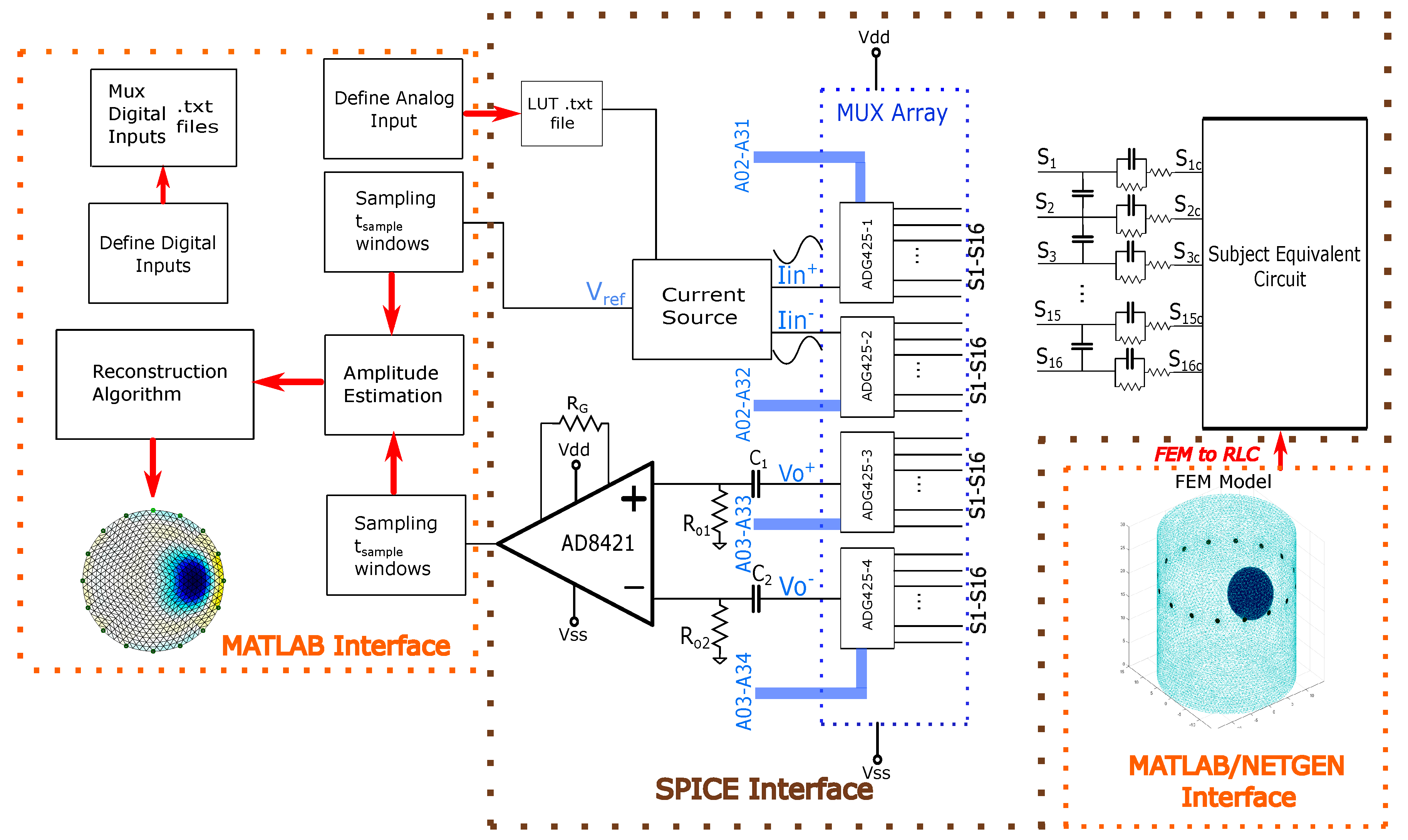
Figure 3. Complete EIT process from phantom to imaging.
Technologies 08 00013 g003
Figure 4. Explanatory graph of the acquisition times pipeline.
Technologies 08 00013 g004
Figure 5. (a) 3D Phantom FEM structure model (b) Low salt conductivity distribution (c) Moderate salt conductivity distribution per element.
Technologies 08 00013 g005
Figure 6. EIT image reconstructions. (a,b): Ideal cases (from FEM simulated measurements-Case T1). (a): Low salt concentration, (b): Moderate salt concentration. (cf): Single-Ended VCCS for f i n = 15 kHz (cases T2a–T2d).(gj): Mirrored VCCS for f i n = 15 kHz (cases T3a–T3d). (kn): Mirrored VCCS for f i n = 100 kHz (cases T3e–T3h). (o,p): Corrupted image due to 10th electrode disconnection (o) and modified image (p). The target object is indicated with a red circle.
Technologies 08 00013 g006
Figure 7. (a): Logarithmic values of the measurement (M = 208) amplitudes for the low sodium chloride concentrations test cases. (b,c): Diametric Conductivity Plots (DCP) for the 2 sodium chloride concentrations and the corresponding test cases. The target corresponds to the object’s circle’s (Figure 6) diameter.
Technologies 08 00013 g007
Figure 8. Average Reciprocity Errors for cases T2a-d (SE) and T3a-h (M).
Technologies 08 00013 g008
Table 1. Fixed values and tolerances of the components in Figure 1 used for the current source simulations at LT Spice. For all cases R s e n s e and R G were set to 100  Ω and 500  Ω correspondingly.
Component R 1 R 2 R 3 R 4 R 5 R 6 R 7
Value5.11 k Ω 221 k Ω 121 k Ω 97.6 k Ω 97.6 k Ω 100 k Ω 97.6 k Ω
Tolerance (%) 1.00 1.00 1.00 0.10 0.10 0.10 0.10
Component R 8 R a R b R c R d C 1 C 2
Value2.25 k Ω - 6 k Ω 374 Ω 374 Ω 1.5k Ω 1.5 k Ω 1.5 nF68 pF
Tolerance (%) 1.00 1.00 1.00 1.00 1.00 --
Table 2. Simulation parameters and Mean Absolute Percentage Errors (MAPEs) measured for cases T2–T4. In the VCCS cell, “SE” means Single-Ended and “M” Mirrored.
Case T 2 a T 2 b T 2 c T 2 d T 3 a T 3 b T 3 c
C N a + C l - (Low/High)LowLowHighHighLowLowHigh
VCCS (SE/M)SESESESEMMM
f i n (kHz)15151515151515
f s (kSps)240100024010002401000240
M A P E M e a s (%) 12.94 11.62 53.37 33.77 9.31 7.03 25.14
M A P E I m a g (%) 219.66 163.70 845337 234.83 145.47 190.45
Case T 3 d T 3 e T 3 f T 3 g T 3 h T 4 a T 4 b
C N a + C l - (Low/High)HighLowLowHighHighLowLow
VCCS (SE/M)MMMMMMM
f i n (kHz)151001001001001515
f s (kSps)1000100020001000200010001000
M A P E M e a s (%) 18.46 19.76 17.60 55.03 48.67 200.86 94.55
M A P E I m a g (%) 196.24 437 242.11 328 284.86 325 221.02