Article

High Throughput Implementation of the Keccak Hash Function Using the Nios-II Processor †

Department of Electrical and Computer Engineering, University of Western Macedonia, 50131 Kozani, Greece
*
Author to whom correspondence should be addressed.
This paper is an extended version of our paper published in 8th International Conference on Modern Circuit and System Technologies on Electronics and Communications (MOCAST 2019), Thessaloniki, Greece, 13–15 May 2019.
Technologies 2020, 8(1), 15; https://doi.org/10.3390/technologies8010015
Submission received: 21 December 2019 / Revised: 5 February 2020 / Accepted: 6 February 2020 / Published: 10 February 2020
(This article belongs to the Special Issue MOCAST 2019: Modern Circuits and Systems Technologies on Electronics)

Abstract

:
Presently, cryptographic hash functions play a critical role in many applications, such as digital signature systems, security communications, protocols, and network security infrastructures. The new standard cryptographic hash function is Secure Hash Algorithm 3 (SHA-3), which is not vulnerable to attacks. The Keccak algorithm is the winner of the NIST competition for the adoption of the new standard SHA-3 hash algorithm. In this work, we present hardware throughput optimization techniques for the SHA-3 algorithm using the Very High Speed Integrated Circuit Hardware Description Language (VHDL) programming language for all output lengths in the Keccak hash function (224, 256, 384 and 512). Our experiments were performed with the Nios II processor on the FPGA Arria 10 GX (10AX115N2P45E1SG). We applied two architectures, one without custom instruction and one with floating point hardware 2. Finally, we compare the results with other existing similar designs and found that the proposed design with floating point 2 optimizes throughput (Gbps) compared to existing FPGA implementations.

1. Introduction

Science of cryptography is the information protection technique to encrypt, store and secure data when transmitted, to prevent reading of private information by intruders or public. Cryptography provides many security enchantments to obviate a security problem and is widely used today, due to its assurance benefits. Critical aspects of cryptography are to offer control, integrity, confidentiality, non-disclaimer, and authentication of the data. Cryptography is a prominent technique used extensively in security.
In recent years, security has been a critical issue in many security applications, such as networking, communication and data authentication in systems. Due to the rapid development of the Internet, security such as authentication must be implemented and maintained to ensure the integrity of information. Hash functions are used in authentication mechanisms, such as the Hashed Message Authentication Code (HMAC) [1], Digital Signatures [2], Secure Electronic Transactions (SET) [3], Public Key Infrastructure (PKI) [4] and network security [5,6].
Presently, legacy architectures of hash functions are ideal candidates for attack using modern cryptanalysis techniques. Serious attacks against SHA-1 were published in [7]. After the successful attacks on SHA-1, it was decided by the NIST to move to SHA-2. The SHA-2 function include in the same general hash function family of SHA-1 so that similar cryptanalysis methods could succeed in the attack [8].
This has led the National Institute of Standards and Technology (NIST) to look for new and safer hashing algorithms. Thus, a new cryptographic hash function standard, the Secure Hash Algorithm 3 (SHA-3), has been developed that offers a high level of security. SHA-3 is based on the Keccak algorithm and adopted as a standard by NIST [9].
In our conference paper [10] we implemented the SHA-2 hash algorithm as a custom hardware accelerator, in three different architectures: without custom instruction, with floating point 1 and floating point 2 Intel IP cores. Our architectures are implemented on a Altera DE2-115 Development and Education Board carrying a Cyclone IV E (EP4C115F29C7) architecture and use a Nios II soft core processor. The results showed, at the speed of the SHA-2 hash algorithm increased by 7% and 11% and the count of cycles reduced by 8% and 14%, respectively.
In this paper, we have enhanced our original research with the following key ideas, techniques and methodologies. We designed the SHA-3 algorithm in the Keccak hash function for all proposed output lengths (224, 256, 384 and 512) in the Intel FPGA Arria 10 GX (10AX115N2P45E1SG). We implemented the SHA-3 algorithm with VHDL programming language. We researched two architectures: the first was without custom instruction and the second was with floating point hardware 2. We designed the two architectures with common evaluation criteria such as frequency, throughput, area, efficiency. Finally, we compared our results with similar published Keccak architectures, found out that they outperform in terms of throughput and efficiency.
The main contributions of the paper are summarized as follows:
  • We designed the Keccak core solution for all the output lengths of the algorithm (224, 256, 384, and 512).
  • We researched on the optimization strategy for the throughput and efficiency of all output lengths of the Keccak algorithm (SHA-3).
  • We performed extensive analysis and compared the throughput and efficiency of our proposed method with other similar methods.
  • For the first time, to the best of our knowledge, we provide extensive estimation of performance and power analysis for all the output lengths for the SHA-3 algorithm.
The structure of the paper is organized as follows. In Section 2, we refer to an overview of research works similar to ours. In Section 3, we briefly present the Keccak Hash Function. In Section 4, we give an outline of the procedure followed for implementing SHA-3 on FPGA. In Section 5, we present the results of our work. Finally, in Section 6 we summarize the conclusions of our research.

2. Related Work

Many researchers proposed several models of the Keccak hash algorithm targetting FPGA devices, to improve throughput, efficiency, area reduction, and power consumption. However, there is still a need to improve throughput and efficiency. Research in security is a vivid domain and this is evident from the plethora of interesting publications. Here, we highlight the ones best connected with our research.
In [11], the authors deal with the performance efficient SHA-3 candidates implemented in the hardware. The main purpose of their work is to compare the hash functions using area and throughput. In their research they use Xilinx FPGA. The throughput achieved for the Keccak hash function is 11.9 Gbps and the covered area (Slices) is 4745. We achieve better results both in the area and throughput.
On this work [12], the authors propose a pipelined Keccak architecture. The proposed Keccak architecture is implemented on a Xilinx FPGA platform (Virtex-5) and simulated in ModelSim. The results show that the proposed architecture achieves good results in frequency and throughput. Our implementation achieves better results in both frequency and throughput.
In [13], the authors address the computational efficiency of SHA-3 candidates in the material. The main purpose of their work is to compare the effectiveness of architectures for the fragmentation functions per unit area. Their research is carried out with the Virtex-5 FPGA. The results showed that the proposed architecture achieves good efficiency and throughput. We achieve better results in both efficiency and throughput.
The authors in [14] propose pipelined, parallel and re-timed architectures in order to increase efficient and throughput hardware implementations of the Keccak algorithm. The proposed architectures are implemented on Spartan-3, Virtex-2 and Virtex-4 devices. The results show that the proposed architectures achieve good results in efficient and throughput. Our implementation achieves better results in both efficient and throughput.
Compact FPGA implementations of the five SHA-3 finalists are given by kerckhof et al. [15]. In these implementations, the hash function implemented as a small area coprocessor without using system external or internal memory. In the best case, low area designs limit the internal data path to 64-bit bus widths.
In [16], the authors commit a detailed hardware performance evaluation of the last round SHA-3 candidates (JH, BLAKE, GROESTL, KECCAK, and SKEIN). They synthesize the hardware designs of the 5 algorithms using Virtex-5, 6 and 7 FPGA chips to get area, frequency and throughput results. They illustrated that the KECCAK algorithm outperforms all other SHA-3 finalists algorithms in terms of clock frequency, area, and throughput.
The two implementations which propose [17] the hardware Keccak hash function described in this article, have been implemented in a FPGA Virtex-5 device. The author’s design approaches include the use of DSP blocks that result in minimal use of traditional logical user, such as lookup tables (LUTs), pipelining that lead to increased time efficiency and combination of the two techniques. Their experimental results prove that Keccak implementations using the DSP blocks are an inefficient design method for applications with low complexity requirements.
Evaluation of compact FPGA implementations for all SHA-3 finalists is presented in [18]. He focuses on area-efficiency and he does not rank the candidates by absolute throughput, but rather by the area and the throughput-area ratio. Furthermore, he removed the need for extra memory as it used by the other authors and added 25 * r / d additional clock cycles.
Finally, Pereira et al. [19] present a technique for paralel processing on FPGA and GPU of the Keccak hash algorithm. They provide the core functionality and the evaluation is performed on an Xillinx Virtex 5 FPGA. However, the results of the pipeline architecture show that the throughput is 7.7 GB and the efficiency is 2.47 Mbps/Slices at output length r = 576 achieving worse results than our implementation at the same output length.
All these research projects are aimed at increasing the throughput of the cryptographic hash function Keccak. In contrast with these authors, we present two architectures of the SHA-3 algorithm in Keccak hash function, using the Nios-II processor. The first architecture is without custom instruction and the second is with floating point hardware 2. The two techniques proposed in this document provide a secure SHA-3 algorithm in Keccak hash function. Our proposed design, using floating point hardware 2, optimizes throughput (Gbps) and efficiency (Mbps/Slices) compared to existing FPGA implementations.

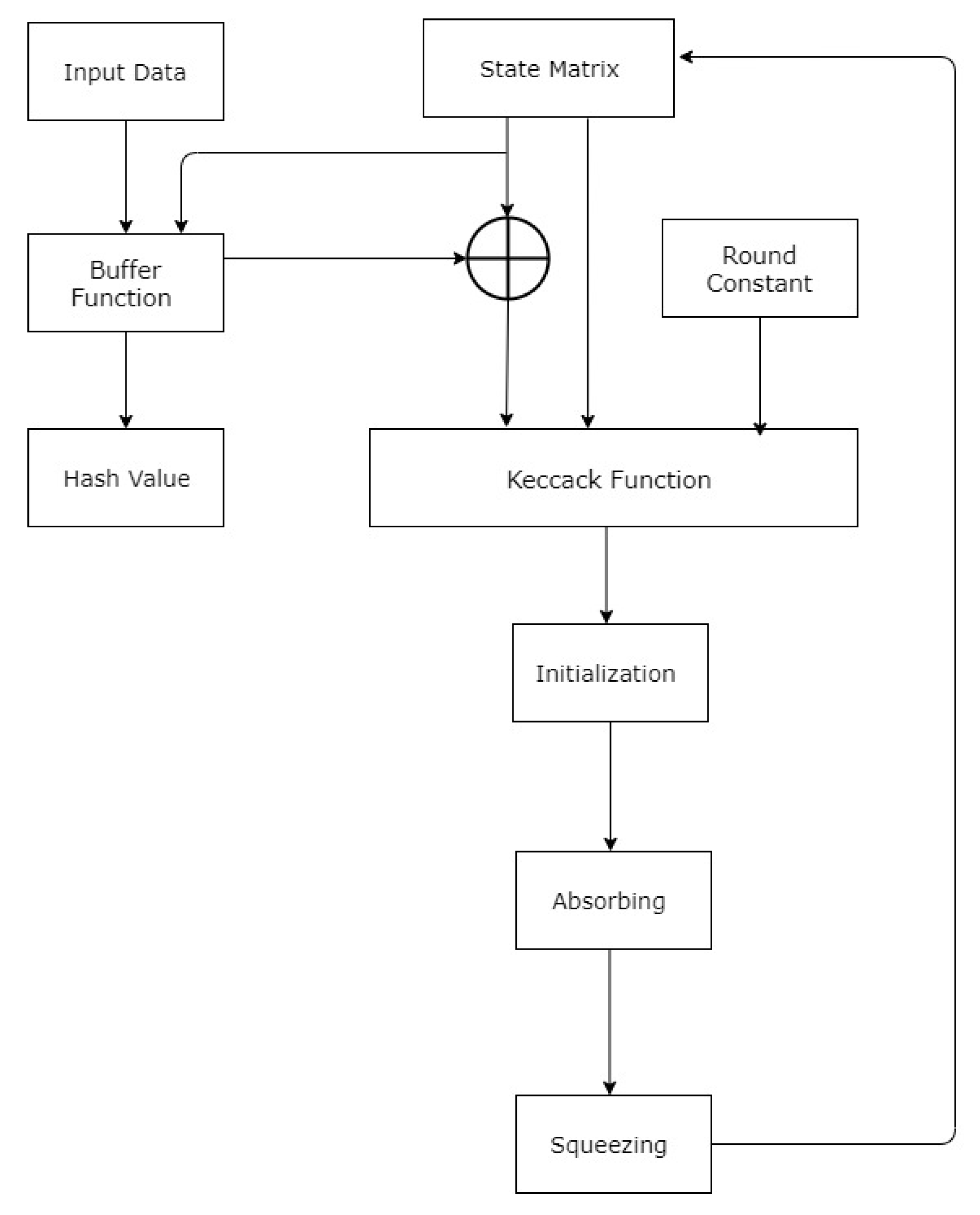
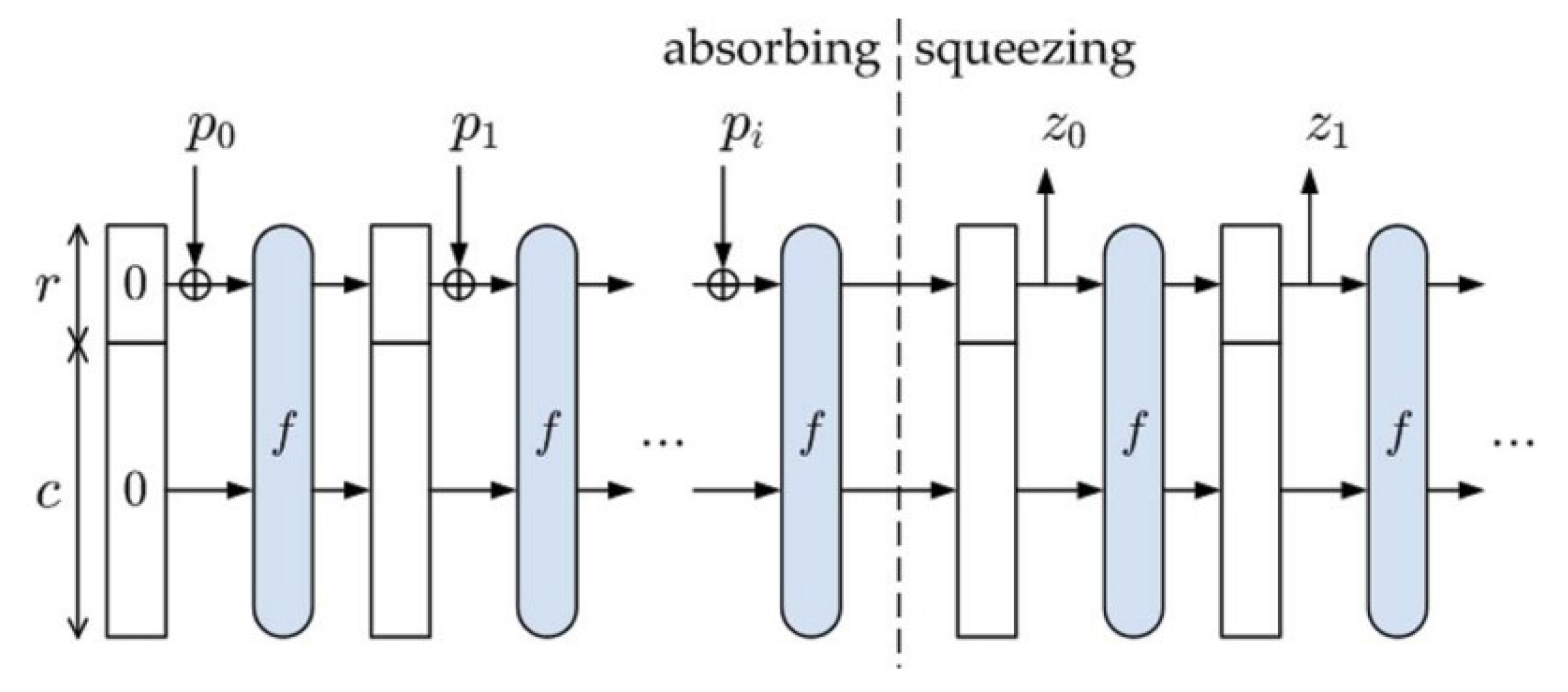
3. Keccak Hash Function
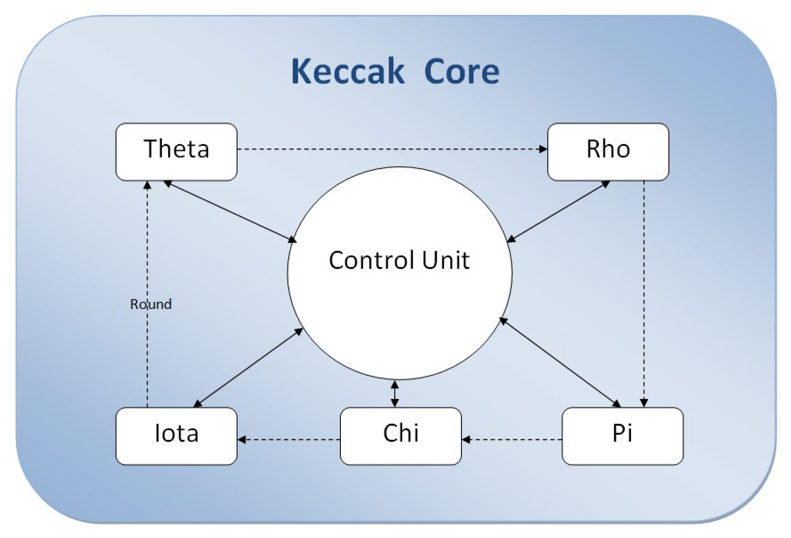
Keccak is a hash function consisting of four cryptographic hash functions and two extendable-output functions. These six functions are based on an approach called sponge functions. Sponge functions provide a way to generalize cryptographic hash functions to more general functions with arbitrary-length outputs [20].
The block diagram of SHA-3 consists of four functional blocks called state function, round constant, buffer function and Keccack function as shown in Figure 1. The algorithm receives as a matrix, an input called state. The state has a length of 1600 bits and consists of a three dimensional 5 × 5 × word-size table, where word-size { 1 , 2 , 4 , 8 , 16 , 32 , 64 } . The buffer function has two input parameters, the first is the number of bits (64 bits or 256 bits) that accepts as input data, and the second is the state matrix and generates hash output based on sponge construction. Depending on the desired output length, the algorithm uses two parameters for the sponge construction as shown in Figure 2.
The two input parameters are the bitrate with r-bits, and the capacity with c-bits which determines the attainable security level. The input message is padded and divided into blocks of r-bits. Function f is the main processing part and consists of 24 rounds with processes. The function f acts on a state, with width b = r + c where r is the outer state and c is the inner state.
The processes of function f are t h e t a , r h o , p i , c h i and i o t a denoted as θ , ρ , π , χ and ι respectively, in a state matrix A. T h e t a , as shown in Equation (1), consists of a parity computation, a rotation of one position, and a bitwise XOR.
C [ x ] = A [ x , 0 ] A [ x , 1 ] A [ x , 2 ] A [ x , 3 ] A [ x , 4 ] 0 x 4 Theta ( θ ) : D [ x ] = C [ x 1 ] ROT ( C [ x + 1 ] , 1 ) 0 x 4 A [ x , y ] = A [ x , y ] D [ x ] 0 x , y 4
R h o in Equation (2) is a rotation by an offset that depends on the word position, and p i is a permutation.
Rho ( ρ ) Pi ( π ) : B [ y , 2 x + 3 y ] = ROT ( A [ x , y ] , r [ x , y ] ) 0 x , y 4
C h i in Equation (3) consists of bitwise XOR, NOT, and AND gates.
Chi ( χ ) : A [ x , y ] = B [ x , y ] ( ( N O T B [ x + 1 , y ] ) A N D ( B [ x + 2 , y ] ) ) 0 x , y 4
Finally, i o t a in Equation (4) is a constant round addition.
lota ( ι ) : A [ 0 , 0 ] = A [ 0 , 0 ] R C
When these five processes are completed, a round is completed. The Padding function complements the bits to be processed.
The Keccak function has three different stages, initialization, absorption, and squeezing. In the absorption phase, the r-bit input message blocks are XORed with the first r-bit of the state and the resulting outputs are interrelated with the function f. When all message blocks are processed, the sponge’s construction changes to the compression phase. In the compression phase, the first r-bit of the state is returned as an output block and is also inserted with the function f. The number of output blocks can be arbitrary and selected by the user.
The Round Constant function R C [ i ] are given in Table 1 and consists of 24 permutations values that assign 64 bit data to Keccak function. The NIST standard defines the following four versions of the Keccak sponge function [2] for message M and output length d as shown in Table 2. More information about Keccak algorithm can be found in [21].

4. Implementation

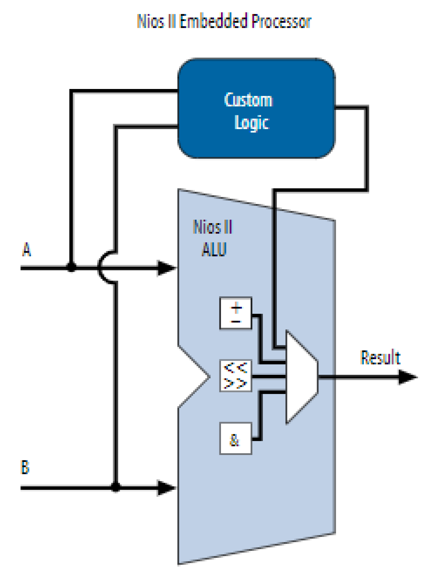
4.1. Nios II Embedded Processor

Nios II is the integrated soft core processor for the Intel FPGA family [22]. The first Nios processor was 16 bit, while the later successor Nios II is 32 bit. According to the Nios original architecture, Nios II presents several enhancements. Nios II is considered to be suitable for most embedded applications (e.g., from DSP to control). Similarly, the Xilinx processor family incorporates a similar competitive softcore CPU with Nios, MicroBlaze.
The advantage of Nios II over MicroBlaze is that it is licensed through a third IP provider for basic ASICs and their simulation in Synopsys Designware. Figure 3 show operation of the Nios II embedded processor and how it connects to external custom logic units.

4.2. Floating Point Hardware 2

The Floating Point Hardware 2 (FPH2) [23] component provides low cycle count implementations of add, sub, multiply, and divide operations, and custom instruction implementations of additional floating point operations. The FPH2 component is the preferred floating point implementation for the Nios II processor. Intel recommends FPH2 rather than the legacy FPH1 because it provides better performance and a smaller device footprint. Table 3 shows a list of the floating operations implemented by each custom instruction.

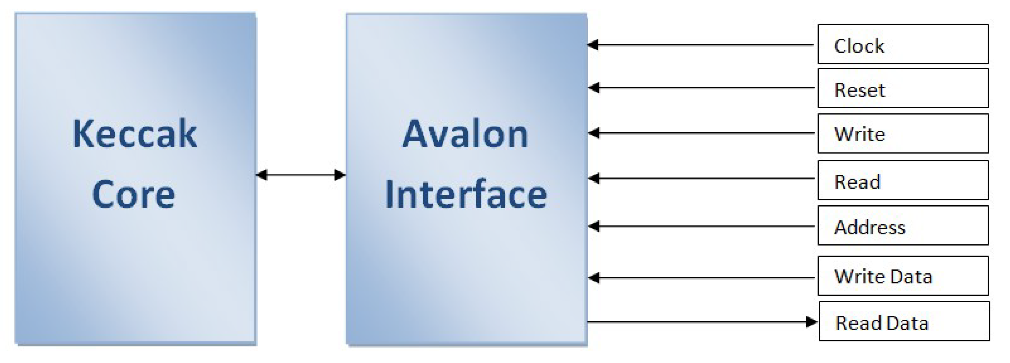
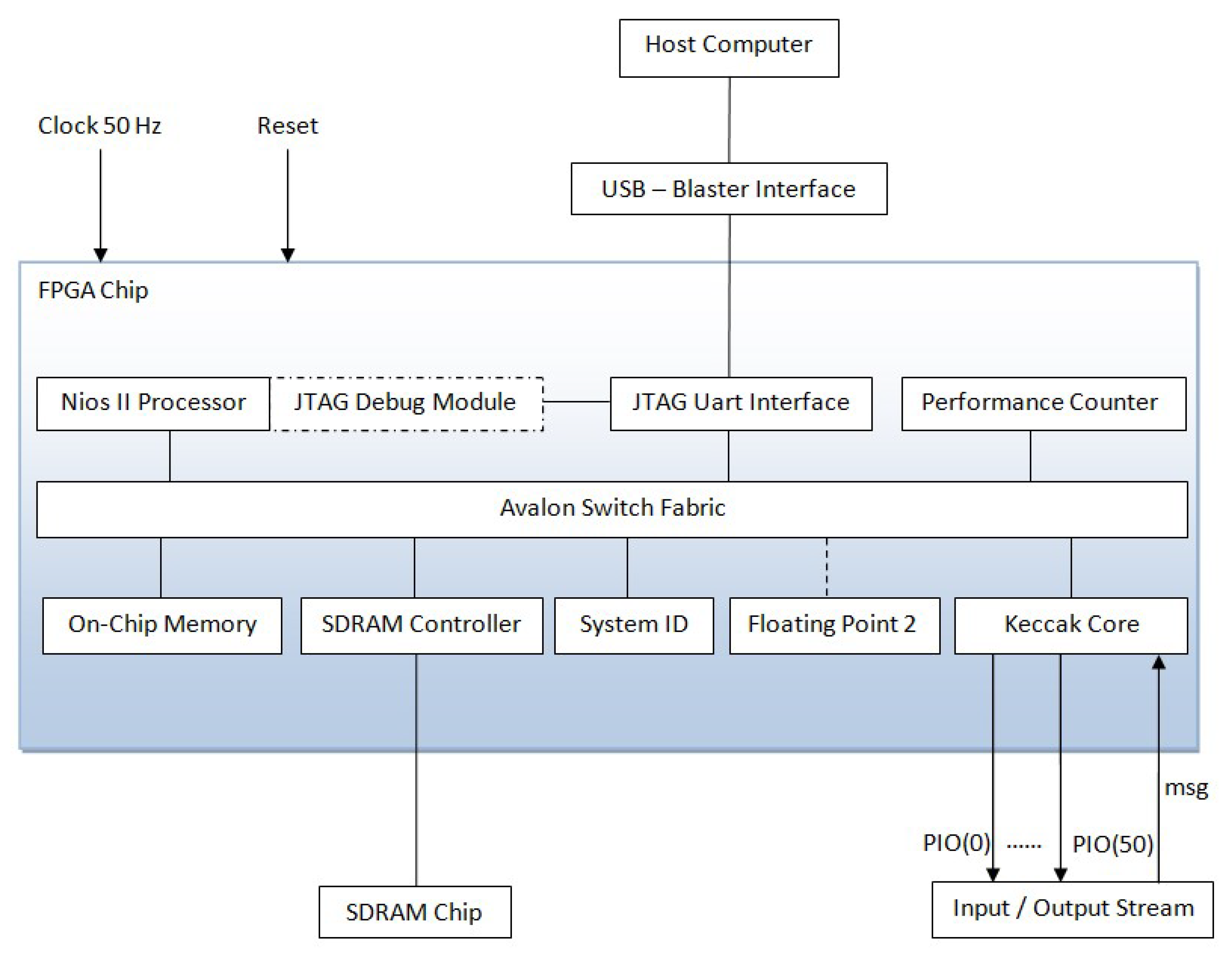
4.3. System Integration

In this work, we focused on reducing the number of clock cycles using floating point hardware 2 in order to achieve higher throughput and efficiency. Additionally, in our architectures, we took into consideration all the output lengths of the Keccak hash algorithm.
In our experiments we used Quartus II version 18.1 Standard Edition software on Windows 10 Professional 64-bit, Intel Core i7-7820X (3.60 GHz) CPU, 32 GB DDR4 SDRAM and Terasic DE5a-Net board. Table 4 and Figure 4 show the specifications of the DE5a-Net board [24] that were used for the SHA-3 implementation.
The SHA-3 algorithm was implemented in the Keccak hash function using the VHDL programming language. Each individual VHDL file was examined separately to verify its functionality. All tests were performed using the ModelSim 10.6d simulator. Then, in the top module, we designed and created block diagrams of all individual VHDL files. We then simulated the top module using ModelSim with valid input samples given in [25]. After verifying the simulation results, we proceeded to design the Nios II.
The Keccak core supports all the output lengths of the Keccak algorithm (224, 256, 384, and 512). The Keccak core block performs the most important function throughout our system design. The Keccak core has 24 permutation rounds and each round consists of five sequential phases called T h e t a , R h o , P i , C h i and I o t a denoted as θ , ρ , π , χ and ι respectively as Figure 5 shows. Keccak takes each stage the state array and after applying the corresponding stage function, returns a new updated state array. The Keccak core has the Control Unit, which is a Finite-State Machine (FSM). The FSM consists of 5 states:
  • S1 for instance choice
  • S2 for main computing
  • S3 for hash computing
  • S4 for rounds
  • S5 for last round
The design of the Nios II was done using the platform designer. The design of the components of the system that we implemented, includes Clock, System ID peripheral, On-chip RAM, Parallel Input Output (PIOs), JTAG-UART, performance counter, DDR4 SDRAM controller, PLL, and Keccak component. The Nios II processor uses On-chip RAM as operating memory. All data is transferred from Nios II to Keccak component via Avalon Switch Fabric, as shown in Figure 6. Figure 7 shows the entire design of our system that we implemented with the Nios II processor.
Then, using the Pin Planner tool we outsourced the connections for SDRAM, PIOs and system clocks. Finally, the implemented system design was applied in the FPGA Arria 10 GX (10AX115N2F45E1SG). By the synthesis report, we get the detailed results for the entire system design we implemented, such as logic use, total registers, total pins, total block memory bits, total DSP blocks and total PLLs.

5. Experimental Results

Experiments have been performed in real hardware using FPGA Arria 10 GX (10AX115N2P45E1SG). The SHA-3 algorithm has been implemented in the Keccak hash function using the VHDL programming language and the Nios II processor was used for all Keccak algorithm output lengths (224, 256, 384 and 512).

5.1. Synthesis Report

We implemented architecture without custom instruction and floating point architecture with floating point 2. By the synthesis report we extracted the detailed results for the entire system design we had implemented the SHA-3 algorithm with the Keccak hash function. Results of the synthesis of the two architectures are presented in Table 5.

5.2. Throughput and Efficiency Results

The evaluation of the SHA-3 algorithm in the Keccak hash function is performed with three metrics of frequency, area, and throughput.
Throughput signifies the number of bits processed per unit time and is specified in Gbps or Mbps. The T h r o u g h p u t is calculated theoretical using Equation (5). In Equation (5), the N o . o f b i t s processed is the bitrate size ‘r’, f r e q u e n c y is the maximum frequency reported by the tool and N o . o f c l o c k c y c l e s after which output is generated. Clock cycles represent the number of iterations needed of the five functions T h e t a , R h o , P i , C h i and I o t a to generate the hash value.
Throughput = No . of bits × frequency No . of clock cycles
The Efficiency is calculated by using Equation (6).
Efficiency = Throughput Area
Table 6 shows the results of our two architectures. The maximum clock frequency is 692 MHz in both architectures. In the implementation without Custom Instruction the clock number of the five functions is 27 while in the implementation with floating point hardware 2 it is 24. A r e a use is specified with respect to number of slices. Every slice of Arria 10 GX FPGA contains four logic (in ALMs) and eight storage elements.
Table 7 and Table 8 show the comparison with other similar architectures, getting the best proposed implementation, in terms of throughput and efficiency. The existing implementations we have found, support the results of their research by simulating Modelsim so our implementation shows, in some cases, an increase in Area (Slices).
The proposed design with floating point hardware 2 achieves the highest throughput and efficiency, compared to the optimum implementations of other similar architectures. The results show that our architecture achieves a reduction in the number of clock cycles.

5.3. Power Analysis EPE

The power analysis for the DE5a-Net DDR4 board from the implementation of the SHA-3 in Keccak hash function is given in Table 9. The temperature rating for the DE5a-Net DDR4 board based on the provided thermal parameters is 22.1 °C. The maximum ambient temperature that the DE5a-Net DDR4 board can handle without breaking the maximum temperature junction is 95.8 °C. The thermal power consumed is 0.018 W. The thermal power dissipated on the chip is 0.766 W. The total thermal power of all resources is 0.784 W. Power analysis was performed using the Intel tool Early Power Estimators (EPE) [26].

6. Conclusions and Future Work

The attacks on SHA-1 led to transition of the SHA-2. The functions of SHA-2 belong to the same class of hash functions as SHA-1, so NIST decided to adopt a new and safer hash algorithm. The newly selected cryptographic hash function standard is the SHA-3. The Keccak hashing algorithm considered the safest up to date and has strong resistance to cryptanalysis attacks as well as high hardware description performance.
In this paper, we focused on the high throughput of the Keccak hash algorithm using the Nios II processor in the FPGA Arria 10 GX (10AX115N2P45E1SG). We opted for the proposed design for all Keccak algorithm output lengths (224, 256, 384 and 512) using the VHDL programming language. We tested functionality of all individual VHDL files with valid response samples.
We performed a design without any custom instruction and implementation with floating point hardware 2 for all output lengths of the Keccak algorithm. Finally, the results for throughput and efficiency of our architecture with floating point hardware 2 achieved better performance due to the reduced number of clock cycles, at least 12.86% and 12.78% respectively compared to existing designs.
In this paper, we implementing the Keccak algorithm, the winner of competition from NIST and the newly selected cryptographic hash function standard as the SHA-3. For future work, we will implement the other four SHA-3 finalists: blake, Grøstl, jh, and Skein. When trying to design more serial architectures, the possibility to share resources, regular structure of an algorithm, and the ordered memory addressing, are added factors that may influence the performance. The diversity in the architectural implementation of these algorithms can lead us to a guide that shows us the ideal solution for hardware security.

Author Contributions

Conceptualization, A.S.; Formal analysis, T.S.; Investigation, A.S. and T.S.; Methodology, A.S. and T.S.; Project administration, A.S. and M.D.; Supervision, M.D.; Writing—original draft, A.S. and T.S.; Writing—review and editing, T.S. and M.D. All authors have read and agreed to the published version of the manuscript.

Funding

This research received no external funding.

Acknowledgments

Intel very kindly donated to our research team a Terasic DE5a-Net Arria 10 GX FPGA Development Kit and 30 floating license, though the Intel FPGA University Program. In this article, we document our experiments with this FPGA board.

Conflicts of Interest

The authors declare no conflict of interest.

Abbreviations

The following abbreviations are used in this manuscript:
SHASecure Hash Algorithm
NISTNational Institute of Standards and Technology
VHDLVery High Speed Integrated Circuit Hardware Description Language
FPGAField-Programmable Gate Array
FPHFloating Point Hardware
GbpsGigabits per second
HMACHashed Message Authentication Code
SETSecure Electronic Transactions
PKIPublic Key Infrastructure
IPIntellectual Property
DSPDigital Signal Processing
LUTslookup tables
GPUGraphics Processing Unit
MbpsMegabits per second
GBGigabytes
RCRound Constant
CPUCentral Processing Unit
ASICApplication-Specific Integrated Circuit
GHzGigahertz
DDR4Double Data Rate 4
SDRAMSynchronous Dynamic Random-Access Memory
SO-DIMMSmall Outline Dual In-line Memory Module
MHzMegahertz
FSMFinite-State Machine
PIOParallel Input Output
JTAGJoint Test Action Group
UARTUniversal Asynchronous Receiver Transmitter
PLLPhase Locked Loop
USBUniversal Serial Bus
ALMAdaptive Logic Module
CCelsius
WWatt
EPEEarly Power Estimators

References

  1. Turner, J.M. The keyed-hash message authentication code (HMAC). In Federal Information Processing Standards Publication; US Department of Commerce, National Institute of Standards and Technology: Gaithersburg, MD, USA, 2008; pp. 191–198. [Google Scholar]
  2. Dang, Q. Recommendation for Applications Using Approved Hash Algorithms; US Department of Commerce, National Institute of Standards and Technology: Gaithersburg, MD, USA, 2008. [Google Scholar]
  3. Jarupunphol, P.; Buathong, W. Secure Electronic Transactions (SET): A case of secure system project failures. Int. J. Eng. Technol. 2013, 5, 278. [Google Scholar] [CrossRef] [Green Version]
  4. Kuhn, D.R.; Hu, V.C.; Polk, W.T.; Chang, S.J. Introduction to Public Key Technology and the Federal PKI Infrastructure; Technical Report for National Institute of Standards and Technology: Gaithersburg, MD, USA, 2001. [Google Scholar]
  5. Loshin, P. IPv6: Theory, Protocol, and Practice; Elsevier: Amsterdam, The Netherlands, 2004. [Google Scholar]
  6. Thomas, S. SSL and TLS Essentials; Wiley: Hoboken, NJ, USA, 2000; p. 3. [Google Scholar]
  7. Wang, X.; Yin, Y.L.; Yu, H. Finding Collisions in the Full SHA-1; Springer: Berlin/Heidelberger, Germany, 2005; pp. 17–36. [Google Scholar]
  8. Radack, S. Secure Hash Standard: Updated Specifications Approved and Issued as Federal Information Processing Standard (FIPS) 180-4; Technical Report for National Institute of Standards and Technology: Gaithersburg, MD, USA, 2012. [Google Scholar]
  9. Dworkin, M.J. SHA-3 Standard: Permutation-Based Hash and Extendable-Output Functions; Technical Report for National Institute of Standards and Technology: Gaithersburg, MD, USA, 2015. [Google Scholar]
  10. Sideris, A.; Sanida, T.; Dasygenis, M. Hardware Acceleration of SHA-256 Algorithm Using NIOS-II Processor. In Proceedings of the 2019 8th International Conference on Modern Circuits and Systems Technologies (MOCAST), Thessaloniki, Greece, 13–15 May 2019; pp. 1–4. [Google Scholar]
  11. Kitsos, P.; Sklavos, N. On the hardware implementation efficiency of SHA-3 candidates. In Proceedings of the 2010 17th IEEE International Conference on Electronics, Circuits and Systems, Athens, Greece, 12–15 December 2010; pp. 1240–1243. [Google Scholar]
  12. Mestiri, H.; Kahri, F.; Bedoui, M.; Bouallegue, B.; Machhout, M. High throughput pipelined hardware implementation of the KECCAK hash function. In Proceedings of the 2016 International Symposium on Signal, Image, Video and Communications (ISIVC), Tunis, Tunisia, 21–23 November 2016; pp. 282–286. [Google Scholar]
  13. Baldwin, B.; Byrne, A.; Lu, L.; Hamilton, M.; Hanley, N.; O’Neill, M.; Marnane, W.P. FPGA implementations of the round two SHA-3 candidates. In Proceedings of the 2010 International Conference on Field Programmable Logic and Applications, Milano, Italy, 31 August–2 September 2010; pp. 400–407. [Google Scholar]
  14. Akin, A.; Aysu, A.; Ulusel, O.C.; Savaş, E. Efficient hardware implementations of high throughput SHA-3 candidates keccak, luffa and black midnight wish for single-and multi-message hashing. In Proceedings of the 3rd International Conference on Security of Information and Networks, Rostov-on-Don, Russia, 7–11 September 2010; pp. 168–177. [Google Scholar]
  15. Kerckhof, S.; Durvaux, F.; Veyrat-Charvillon, N.; Regazzoni, F.; de Dormale, G.M.; Standaert, F.X. Compact FPGA implementations of the five SHA-3 finalists. In Proceedings of the International Conference on Smart Card Research and Advanced Applications, Athens, Greece, 12–15 December 2010; pp. 217–233. [Google Scholar]
  16. Jararweh, Y.; Tawalbeh, H.; Moh’d, A. Hardware performance evaluation of SHA-3 candidate algorithms. J. Inf. Secur. 2012, 3. [Google Scholar] [CrossRef] [Green Version]
  17. Provelengios, G.; Kitsos, P.; Sklavos, N.; Koulamas, C. FPGA-based design approaches of keccak hash function. In Proceedings of the 2012 15th Euromicro Conference on Digital System Design, Izmir, Turkey, 5–8 September 2012; pp. 648–653. [Google Scholar]
  18. Jungk, B. Evaluation of compact FPGA implementations for all SHA-3 finalists. In Proceedings of the Third SHA-3 Candidate Conference, Washington, DC, USA, 22–23 March 2012. [Google Scholar]
  19. Pereira, F.D.; Ordonez, E.D.M.; Sakai, I.D.; de Souza, A.M. Exploiting Parallelism on Keccak: FPGA and GPU comparison. Parallel Cloud Comput. 2013, 2, 1–6. [Google Scholar]
  20. Bertoni, G.; Daemen, J.; Peeters, M.; Van Assche, G. Cryptographic Sponges Functions. Available online: http://sponge.noekeon.org/CSF-0.1.pdf (accessed on 5 February 2020).
  21. Bertoni, G.; Daemen, J.; Peeters, M.; Assche, G. The keccak reference. Submiss. NIST Round 3 2011, 13, 14–15. [Google Scholar]
  22. Intel®FPGA. Nios® II Processors for FPGAs. Available online: https://www.intel.com/content/www/us/en/products/programmable/processor/nios-ii.html (accessed on 5 February 2020).
  23. Intel®FPGA. Overview of the Floating Point Hardware 2 Component. Available online: https://www.intel.com/content/www/us/en/programmable/documentation/cru1439932898327.html#shd1506201174145 (accessed on 5 February 2020).
  24. Terasic. All FPGA Main Boards-Arria 10-DE5a-Net-DDR4. Available online: https://www.terasic.com.tw/cgi-bin/page/archive.pl?Language=English&No=1108 (accessed on 5 February 2020).
  25. CSDITL-NIST. Example Values—Cryptographic Standards and Guidelines. Available online: https://csrc.nist.gov/projects/cryptographic-standards-and-guidelines/example-values (accessed on 5 February 2020).
  26. Intel®FPGA. Early Power Estimator for Intel® Arria® 10 FPGAs User Guide. Available online: https://www.intel.com/content/dam/www/programmable/us/en/pdfs/literature/ug/ug-01164.pdf (accessed on 5 February 2020).
Figure 1. Block diagram of Keccak algorithm.
Technologies 08 00015 g001
Figure 2. Mechanism of Sponge-Functions.
Technologies 08 00015 g002
Figure 3. Nios II embedded processor with custom logic unit [22].
Technologies 08 00015 g003
Figure 4. Intel DE5a-Net Arria® 10 GX FPGA board (Terasic, Taiwan) [24].
Technologies 08 00015 g004
Figure 5. Keccak Core block diagram.
Technologies 08 00015 g005
Figure 6. Data transfer between Avalon Switch Fabric and Keccak Core.
Technologies 08 00015 g006
Figure 7. The block diagram of the entire system. Nios II system implemented on the DE5a-NET DDR4 board.
Technologies 08 00015 g007
Table 1. The round constants R C [ i ] of keccak algorithm.
RC[0]0x0000000000000001RC[8]0x000000000000008ARC[16]0x8000000000008002
RC[1]0x0000000000008082RC[9]0x0000000000000088RC[17]0x8000000000000080
RC[2]0x800000000000808ARC[10]0x0000000080008009RC[18]0x000000000000800A
RC[3]0x8000000080008000RC[11]0x000000008000000ARC[19]0x800000008000000A
RC[4]0x000000000000808BRC[12]0x000000008000808BRC[20]0x8000000080008081
RC[5]0x0000000080000001RC[13]0x800000000000008BRC[21]0x8000000000008080
RC[6]0x8000000080008081RC[14]0x8000000000008089RC[22]0x0000000080000001
RC[7]0x8000000000008009RC[15]0x8000000000008003RC[23]0x8000000080008008
Table 2. SHA3 instances.
InstanceOutput Size dRate r-Block SizeCapacity c
SHA3-224(M)2241152448
SHA3-256(M)2561088512
SHA3-384(M)384832768
SHA3-512(M)5125761024
Table 3. Floating operations implemented by each custom instruction.
Floating Point Hardware 2 Component
(altera_nios_custom_instr_floating_point_2)
Combinatorial Custom Instruction
(altera_nios_custom_instr_floating_point_2_combi)
Multi-Cycle Custom Instruction
(altera_nios_custom_instr_floating_point_2_multi)
minimum
maximum
compare
negate
absolute
add
subtract
multiply
divide
square root
convert
Table 4. Intel Arria® 10 GX FPGA Specifications.
ParametersValues
FamilyIntel Arria® 10 GX FPGA
Device10AX115N2F45E1SG
Memory2 × 4 GB DDR4 SO-DIMM 2400 MHz SDRAM
System Clock Frequency50 MHz Oscillator
Table 5. SHA-3 Algorithm with the Keccak hash function synthesis report.
ItemsWithout Custom
Instruction
With Floating
Point Hardware 2
Logic use (in ALMs)11,102/427,200 *
(3%)
12,020/427,200 *
(4%)
Total registers24,51924,568
Total pins370/992 *
(37%)
372/992 *
(38%)
Total block memory bits1,501,453/55,562,240 *
(3%)
1,504,301/55,562,240 *
(3%)
Total DSP Blocks3/1518 *
(<1%)
7/1518 *
(<1%)
Total PLLs7/112 *
(6%)
7/112 *
(6%)
* Denotes the maximum resource in the category.
Table 6. Throughput and Efficiency results of our two architectures.
DesignProposed Design
without Custom
Instruction
Proposed Design
with FPH2
Area (Slices)27763005
Throughput (Gbps)r = 115229.52533.216
r= 108827.88531.370
r= 83221.32323.989
r= 57614.76216.608
Efficiency (Mbps/Slices)r= 115210.6311.05
r= 108810.0410.43
r= 8327.687.98
r= 5765.315.52
Table 7. Throughput results and comparison. With bold is ours experimental results.
DesignFPGAFrequency
(MHz)
Area
(Slices)
Throughput (Gbps)
r = 1152r = 1088r = 832r = 576
Kitsos P. et al.
(2010) [11]
-2154745-11.9--
Mestiri H. et al.
(2016) [12]
Virtex-5317.114793---12.68
Jararweh Y. et al.
(2012) [16]
Virtex-52711414-12.28--
Provelengios G. et al.
(2012) [17]
Virtex-52852573---5.70
Kerckhof S. et al.
(2011) [15]
Virtex-6285188---0.077
Jungk B.
(2012) [18]
Virtex-6197397-1.071--
Baldwin B. et al.
(2010) [13]
Virtex-518911175.9156.2638.1908.518
Pereira F. et al.
(2013) [19]
Virtex-54523117---7.70
Akin A. et al.
(2010) [14]
Virtex-45094356-22.33--
Proposed design
with FPH2
Arria 10 GX692300533.21631.37023.98916.608
Table 8. Efficiency results and comparison. With bold is ours experimental results.
DesignFPGAFrequency
(MHz)
Area
(Slices)
Efficiency (Mbps/Slices)
r = 1152r = 1088r = 832r = 576
Kitsos P. et al.
(2010) [11]
-2154745-2.50--
Mestiri H. et al.
(2016) [12]
Virtex-5317.114793---2.71
Jararweh Y. et al.
(2012) [16]
Virtex-52711414-8.68--
Provelengios G. et al.
(2012) [17]
Virtex-52852573---2.21
Kerckhof S. et al.
(2011) [15]
Virtex-6285188---0.41
Jungk B.
(2012) [18]
Virtex-6197397-2.69--
Baldwin B. et al.
(2010) [13]
Virtex-518911173.003.174.154.32
Pereira F. et al.
(2013) [19]
Virtex-54523117---2,47
Akin A. et al.
(2010) [14]
Virtex-45094356-5.13--
Proposed design
with FPH2
Arria 10 GX692300511.0510.437.985.52
Table 9. Power analysis.
Thermal AnalysisThermal Power (W)
Junction Temp, TJ (°C)22.1HPS0.018
Maximum Allowed TA (°C)95.8PSTATIC0.766
TOTAL (W)0.784

