Review

Review of Converter Circuits with Power Factor Correction

Facultad de Ingeniería, Universidad Distrital Francisco José de Caldas, Bogotá 110231, Colombia
*
Authors to whom correspondence should be addressed.
Technologies 2025, 13(6), 221; https://doi.org/10.3390/technologies13060221
Submission received: 15 April 2025 / Revised: 23 May 2025 / Accepted: 26 May 2025 / Published: 28 May 2025
(This article belongs to the Collection Electrical Technologies)

Abstract

:
This article reviews converter circuits with power factor correction considering issues that arise in implementing such circuits. The Preferred Reporting Items for Systematic Reviews and Meta-Analyses (PRISMA) procedure are employed for the review. Six topologies with power factor correction were considered including boost, buck, buck-boost, Cük, dual boost, and totem pole bridgeless. The main findings highlight various implementation alternatives for these converters, taking into account complexity, performance, control strategies, and applications. Additionally, the review identified studies based on simulation and hardware implementation. Several alternatives exist for research to improve energy conversion circuits using conventional techniques such as PI controllers or novel controllers using artificial intelligence techniques such as neural networks. Finally, it should be noted that converter circuits with power factor correction are crucial for developing various electrical and electronic devices in domestic and industrial applications.

Graphical Abstract

1. Introduction

Electricity plays a fundamental role in the way human beings live. From users in large industries to the network connection of a smartphone in a residence, the quality of the electrical energy delivered to consumers will always be vital. Hence, from electrical engineering (modeling of power systems), and electronic engineering (modeling of power electronic devices), new and better strategies are still being sought to guarantee adequate energy supply [1].
Rectifiers and converters are among the devices that adapt energy to the final consumer and are also key for the design of any electrical source. By combining different topologies (circuit configurations of switching devices, resistors, capacitors, and inductors) different operating ranges can be obtained from the loads desired to be connected to them. Some of the variables to carry out the control operation on the loads range from voltage elevation, voltage reduction, rectification, Power Factor Correction (PFC), ripple reduction, reduction of Total Harmonic Distortion (THD) of the signal, voltage imbalance within the components inherent to the circuit that compose the source, among others. Considering the quantity and complexity of variables to be controlled, it is not surprising the great advantage represented by electronic controller devices functioning as the brain that manipulates the converter components when maintaining the mentioned variables within the desired ranges [1].
Given the efficient energy consumption features, circuits that grant high Power Factor (PF) become of particular interest. For the same active power consumption, the lower the power factor, the greater the current demanded [1].
Regarding some representative works in developing high power factor conversion circuits, authors in [2] study a half-bridge boost rectifier topology with bidirectional switches. In the experimental implementation, a maximum power factor correction of 0.98 was obtained by measurement without zero crossings in the line input current and the highest frequency at the input (500 Hz). In the research of [3], a pulse width control technique is proposed for a half-bridge boost converter with conventional topology established in [4]. The technique used here is based on a proposed algorithm for predicting the duty cycle obtained from the average state and input variables using the Average Circuit Model (ACM). The outcomes obtained a power factor of 0.9954 and a total harmonic distortion of 2 % .
Another work worth considering is presented in [5] proposing a micro inverter for grid-connected photovoltaic systems with a first stage of a half-bridge boost converter and a second stage of a full-bridge inverter. These two stages are coupled using a transformer that galvanically isolates them. Each stage had a control system, achieving an efficiency of up to 98.2 % , a power factor greater than 0.99 , and a THD of a maximum of 2.87 % . In addition, a half-bridge boost converter with galvanic isolation using a transformer is presented in [6]. This study is oriented to using this converter in far wide ranges of regulation of input voltage. An efficiency close to 97 % was obtained.
In the study in [7], a converter composed of two half-bridge AC-DC boost converters is proposed, achieving phase shift operation capability. This approach reduced switching losses under load variations below the nominal consumption power and helps reduce switching losses by half under medium and low loads in this topology. Meanwhile, the performance of PFC in bridged and bridgeless boost converters is presented and analyzed in [8]. The bridgeless PFC converter provides a near-unity power factor, improved efficiency, and lower total harmonic distortion. Finally, research of two LED drivers associated with a power factor correction system and a Half-Bridge LLC Converter (HB-LLC) is displayed in [9].
Considering the importance of having a high power factor to achieve efficient transmission and consumption of electrical energy, research on electrical energy conversion devices with a power factor correction is of utmost importance.

Paper Approach and Organization
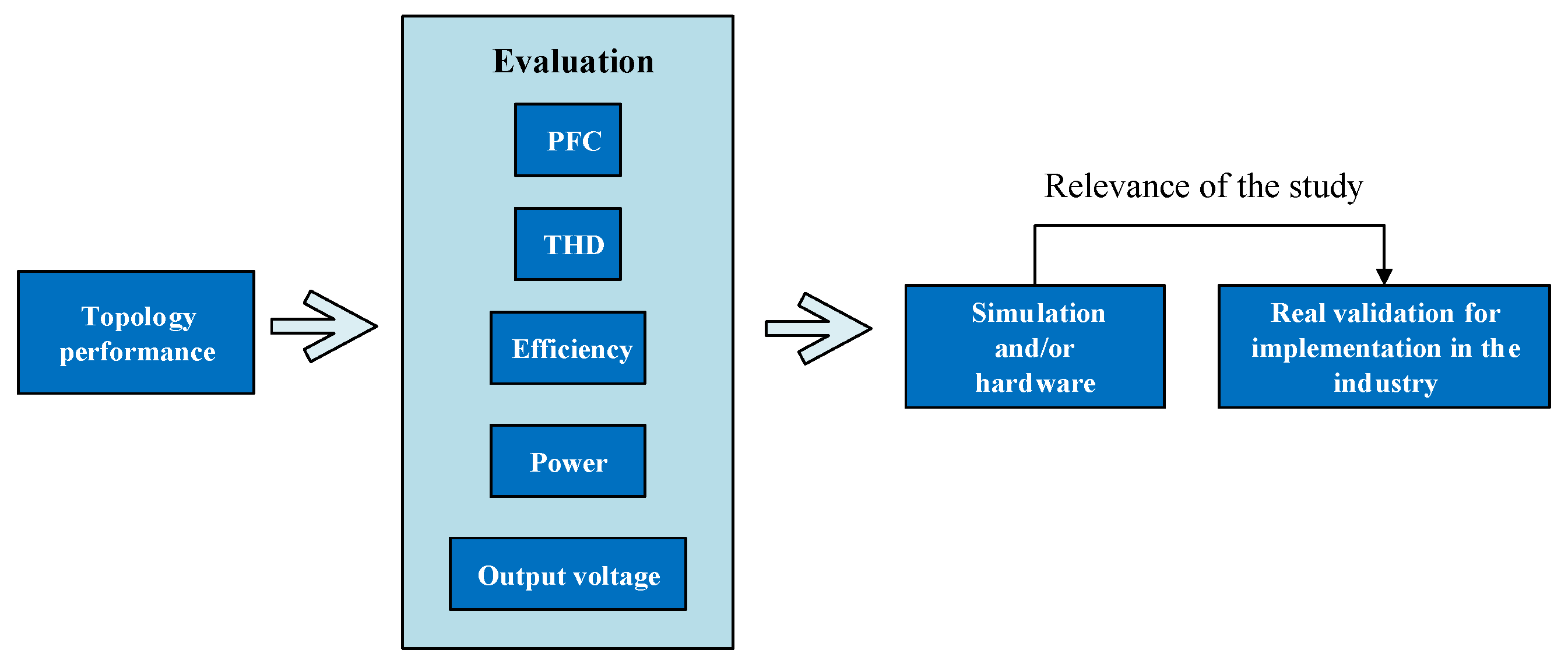
This work aims to develop a review of converter circuits with power factor correction considering different aspects related to implementing converters with power factor correction. The paper approach is displayed in Figure 1. Different articles must be evaluated under the same parameters, allowing for a fair comparison and analysis across topologies to select the most suitable studies within the available topologies. After this, the impact level of the article must be established based on its implementation level, namely, simulation or hardware.
The main motivation of this work is to provide an overview of different implementation alternatives for converters with power factor correction, as power quality is a critical aspect in electrical engineering for supplying power reliably and safely, and for ensuring the proper operation of electrical equipment and devices. Accordingly, this framework aims to identify key aspects to consider when implementing a power converter with power factor correction to achieve high performance in electrical energy conversion.
The paper organization is as follows, Section 2 displays the methodology employed, Section 3 addresses the review of different topologies of power conversion circuits with power factor correction. Finally, the discussion and conclusions are addressed in Section 4 and Section 5.

2. Methodology

The methodology utilized is displayed [10,11] where the information (papers) was collected from different databases, Figure 2 shows the research stages. The first stage reviews the state-of-the-art to identify the aspects related to energy converters with power factor correction employing sources as SCOPUS, Science Direct, MDPI, and IEEE databases in this step.
Gathering and debugging data from databases constitutes the second phase. The PRISMA [12,13] guideline was employed in conjunction with the inclusion criteria stated in Table 1. The information collection and debugging process is shown in Figure 3, where a large group of articles is first gathered, which are labeled as the most relevant for the review after the selection process.
As defined in the PRISMA premise for data collection, the first step consists of finding records in the databases employing Equation (1). The sign * indicates that extra characters can be retained. The sentence structure is preserved as indicated by the quotation marks.
Search-items = ( converter circuits * ) AND                     ( buck * OR boost * OR rectifier * OR power * OR topologies * OR electronics * ) AND ( power factor correction )
The titles, keywords, and abstracts of the papers in the databases were searched using Equation (1). At first, publications were recognized as 43 in IEEE, 36 in MDPI, and 27 in SCOPUS. Documents, including review, scientific, and conference papers (articles), were included in the search, which was conducted on 11 December 2024 (updated to 16 May 2025). The records from the databases were then combined during the selection phase, and any duplicates were eliminated. After that, 81 papers were selected (25 were excluded) after the titles and abstracts of the publications were examined in light of the inclusion and exclusion items. The eligibility step was then carried out, in which all of the documents were examined, and those that did not fit the methodology of the study were discarded. Twenty papers were eliminated during the eligibility stage, while 61 papers were chosen. A qualitative study of the documents is conducted during the inclusion stage, excluding some when necessary. In the final round of inclusion, three papers were excluded out of 58 articles that met the requirements. Therefore, in order to arrive at the findings, the results of the conceptual review and the outcome analysis were used.

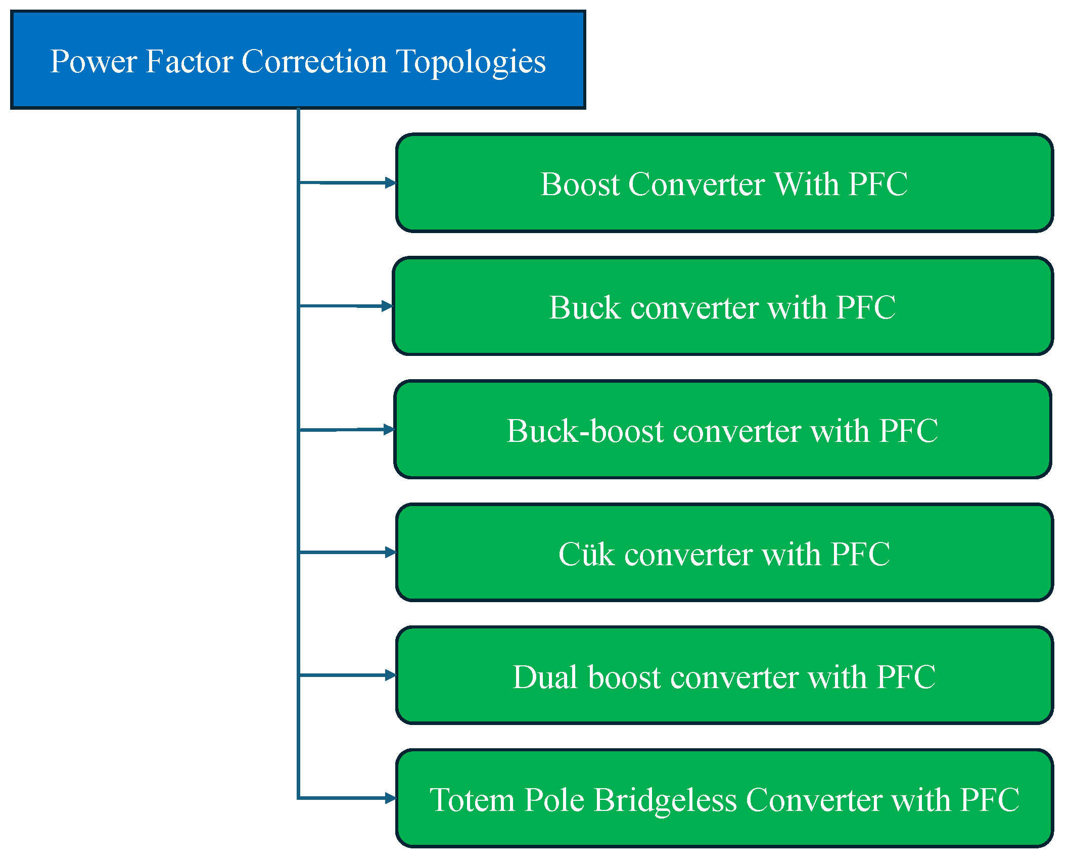
3. Recent Works on Topologies with PFC

This section reviews recent work considering different topologies used to achieve a high power factor in converting electrical energy. Figure 4 shows the different identified topologies of converter circuits with power factor correction. The review considers different aspects related to the implementation of converters with power factor correction.
Boost topology is the most common in PFC applications given its simplicity, highly efficient, and capable of producing a continuous input current that facilitates compliance with power quality regulations. It works by increasing the peak amplitude of the input voltage to a higher value and is widely used in switching power supplies and LED lighting systems. A buck converter reduces the input voltage to a lower output voltage. It works by storing power in an inductor and then releasing it to power the load. This converter has applications in electronic systems where a constant output voltage is required. The buck-boost topology allows the input voltage to be increased and decreased, but reverses the polarity and causes a pulsating input current, generating more electromagnetic interference. However, it is useful in low-power applications with wide line voltage fluctuations. The Cük converter offers continuous power transfer and low current ripple, although the main disadvantage is its reverse output polarity and greater structural complexity; hence, it is more commonly utilized in specific industrial applications. Compared to a traditional boost converter topology, double dual boost converter offers a larger output voltage increase, lower input current ripple, and excellent energy conversion efficiency. This type of converter is especially well-suited for applications that requiere high voltage growth and efficient energy management, such as solar power plants, electric vehicles, and other renewable energy systems. Finally, the totem pole bridgeless converter topology integrates the rectification and boost stages using two switching branches; the additional active switches make the control circuitry more complex. The most common application for this type of converter is charging electric vehicles.
As noted, this review focuses on the main converter topologies employed to achieve a high power factor: the boost, buck, buck-boost, Cük, dual boost, and totem pole bridgeless. Variants of these topologies can be found to generate other sub-classifications. For example, the interleaved boost converter is a variant that employs multiple parallel shift-commutated boost stages, which reduces input current ripple, better distribute heat between components, and increases overall efficiency, making it ideal for high-power applications such as servers and industrial inverters. The bridgeless boost is an improvement on this topology that eliminates the input bridge rectifier, thereby reducing conduction losses allowing noticeably higher efficiency, especially in applications where energy efficiency is critical, such as electric vehicle chargers. Meanwhile, the Single-Ended Primary-Inductor Converter (SEPIC) is similar to the Cük converter since they are composed of two inductors, link capacitors, diode, and switch. They differ primarily in output voltage polarity; the SEPIC is a positive output converter, while the Cük is a negative output converter. The SEPIC also increases or decreases the maximum input voltage amplitude without inverting the output polarity. However, its design requires more passive components, making it unsuitable for automotive environments or sources with widely varying input voltage ranges. The flyback topology can be considered a buck-boost converter, which is commonly used in low-power systems given its simplicity, natural galvanic isolation, and ability to operate as a boost or buck converter, making it a cost-effective option for consumer electronics and compact adapters where integrated PFC is required. Finally, the totem pole bridgeless converter topology has half-bridge and full-bridge applications. The full-bridge topology is widely used in high-power applications allowing for efficient and symmetrical power conversion, supporting high current levels with lower conduction losses per branch. The half-bridge configuration features a simpler conversion circuit with fewer switches. Its main advantage is high efficiency since the switches operation produces only one voltage drop.

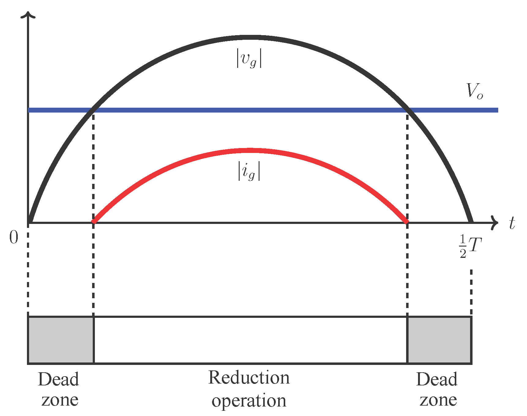
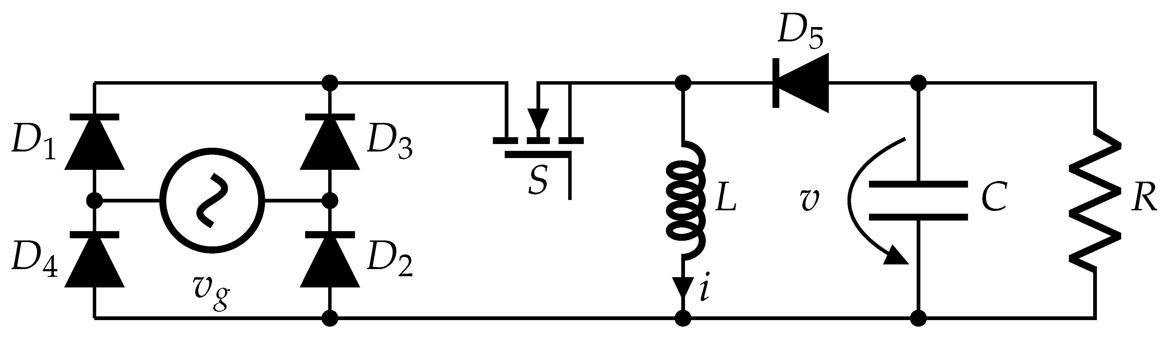
3.1. Boost Converter with PFC

A boost converter increases the input voltage to a higher output voltage. Boost converters are employed in numerous applications, including power supplies, portable devices such as mobile phones and laptops, solar panels, and other renewable energy systems. Regarding the Boost converters, a basic circuit is displayed in Figure 5, the connections between resistance R, inductance L, capacitor C, diode D 5 , and switch S are shown. In this circuit, diodes D 1 to D 4 constitute the rectifier of the alternating voltage source v g . Most of the reviewed work with a PFC approach takes this configuration as a reference.
At times, a lower DC output voltage than the AC input is often needed. In this regard, a two-stage single-phase source consisting of PFC booster topology stage, and a second stage consisting of a step-down converter, which delivers a DC voltage to the load is implemented in hardware [14]. For this case, a load of 1 kW and two operating situations were taken into account: 127 Vac and 100 Vdc, 220 Vac, and 200 Vdc, describing input and output voltages, respectively. This study obtained a maximum efficiency of 96.5 % , a total harmonic current distortion of 4.6 % , and a power factor close to unity.
It is also essential that the system be capable of reducing the effects of electromagnetic interference as much as possible. Considering this situation, in [15], the sliding frequency modulation control for a single-phase boost PFC is implemented in hardware, and its behavior is compared with a conventional constant frequency controller of 120 kHz. The nominal power handled by the converter is 300 W, and efficiencies above 96 % and a THD level of 3.73 % were obtained, which is considerably lower than the 5 % established by the IEEE 519 standard. These results were given for an input of 169.7 V and an output of 383 V.
These converters can be used as light source feeder drivers as presented in [16], where a single-phase boost-flyback topology is proposed. In this study, an actual assembly of an 18 W LED driver is fed, with which a power factor no greater than 0.946 was obtained for both input voltage cases (175 Vac and 250 Vac) and a THD value between 1.5 % and 1.75 % , a PF greater than 0.9375 for a voltage of and an approximate efficiency of 86.5 % for a 220 Vac input. As the input voltage level was increased, the efficiency and PF values decreased to 86 % and 0.938 , respectively (input voltage: 175 250 V). For 175 V and 250 V input, a voltage of 300 V and 430 V is handled, respectively, in the output capacitor of the first stage (boost stage) but always maintaining a final supply voltage for the LED luminaire of 60 V.
From the perspective of applications, power supplies for electric cars have become highly relevant in the last century. That is why in [17], a single-phase battery charger consisting of three stages is implemented in simulation (MATLAB/Simulink): a rectifier bridge, a boost converter, and an LLC resonant converter. The latter is used to accelerate the battery charge. The input voltage varies from 160 Vac to 260 Vac. For the latter, a maximum THD value of 3.06 % and a minimum PF value of 0.99952 were obtained, with a load value of 576 W.
Usually, to improve the input current THD of single-phase PFC converters, increasing the switching frequency and the controller sampling frequency is necessary. This causes the complexity of the control strategy to increase along with the computing power, which is why in [18], a model predictive control for the modulation stage (PWM) is designed and manufactured by adding an extra element to the control loop. This control helps to have an adequate level of THD without increasing the switching and sampling frequency. Using a load of 500 W and an input voltage of 110 V for an input current of 6.8 A and 3.5 A, 3.55 % and 6.59 % of THD were obtained, respectively. The converter output voltage was 250 V.
In [19], a proportional resonant controller for a single-phase interleaved boost PFC converter is implemented in Simulink. With this type of control, an efficiency of 95 % was achieved. Figure 6 displays the standard interleaved boost converter circuit. The input and output voltage of the converter was 177 V and 400 V, respectively. The load utilized in the simulations was 350 W.
In the case of [20], to avoid the design and implementation of a zero-crossing circuit (inductor current) for the limit conduction mode (transition between continuous conduction mode and discontinuous conduction mode), two control strategies with Pulse Frequency Modulation (PFM) are proposed together with a single-phase boost converter topology that inherently has a limit conduction mode. Once the converter was implemented experimentally and the measurements obtained, a PF of 0.99 and a maximum efficiency value of 96.5 % were achieved. The implemented prototype was 120 W, with an input voltage range of 175 V to 265 V, resulting in an output voltage of 400 V.
A relevant challenge for power supplies is to maintain adequate performance for any load value as long as it does not exceed the thresholds for which it was designed. In addition, the effects of the source on the network under these load cases must be considered. In this regard, in [21], a control technique is proposed so that a single-phase boost PFC behaves satisfactorily for low load values. This technique uses a PI controller; the parameters used to implement the prototype are an input voltage of 220 V, an output voltage of 400 V, and a switching frequency of 50 kHz. The maximum load to be connected is 615 W.
According to [22], the simulation results and their implementation in hardware must be obtained to evaluate a boost converter. In addition, different control scenarios must be evaluated to find the best-performing ones under the main characterization factors and thus determine the performance of the plant. In the case of [22], the individual design of five current controllers for a boost converter with single-phase PFC is established: P controller, PI controller, Proportional Resonant (P-RES) controller, PI Resonant (PI-RES) controller, and Repetitive Controller (RC). Under the simulation scenarios, the best controller was the RC, obtaining a power factor and THD of 0.9528 and 32.48 % , respectively. For the most relevant scenario, the actual implementation in hardware, only the P and PI controllers could be applied, the power factor values equal to 0.841 and 0.8674 were measured, respectively. This was due to the lack of computational capacity of the DSP used by the researchers to implement the other three control strategies. The parameters of the implemented converter were input voltage of 12 V, output voltage of 24 V, switching frequency of 80 kHz, and a maximum connection load equal to 6 W.
In the study [23], a simulation comparison was made between the boost converter, Cük, and Zeta (single-phase). The THD level was evaluated under load variation and continuous mode during the current operation. The loads for the three types of converters had values 600 W, 800 W, and 1 kW, resulting in a minimum THD of the three cases equal to 2.55 % (boost converter), 0.75 % (Cük converter), and 3.55 % (Zeta converter). In the boost and Cük topologies, a better THD was obtained by having a higher value in the load (higher power); the opposite case was in the Zeta topology, where the THD level increased as the load increased. All results were obtained from the simulation. An input voltage of 35 V was used for the boost converter and an output voltage varied between 100 V and 130 V according to each load case evaluated (600 W, 800 W, and 1 kW).
In [24], a design strategy for a single-phase PFC boost converter is proposed to guarantee stability at different operating points of the plant. It is also implemented a cascade with a Sliding Mode Controller (SMC) for the inductor current and a PI controller for the output voltage. Once the plant was simulated in the PSIM software, a PF of 0.9997 and a THD of 1.84 % were obtained. This operation was maintained under a switching frequency of 300 kHz, a grid supply voltage equal to 120 Vac, a load voltage equal to 220 Vdc, and a maximum output power of 440 W.
Likewise, different techniques for designing and manufacturing single-phase PFC power supplies in hardware are presented in [25], where small-signal stability modeling is used. This power supply design is oriented to telecommunication applications. Considering supply voltages of 176 264 Vac and output voltages of 320 410 Vdc, the following results were obtained by simulation:
  • Load of 500 W: FP equal to 0.99 , and THD of 6.57 % .
  • Load of 750 W: FP equal to 0.9945 , and THD of 5.96 % .
  • Load of 1250 W: FP equal to 0.9955 , and THD of 5.15 % .
  • Load of 2000 W: FP equal to 0.9935 , and THD of 5.5 % .
Specific methods for implementing a controller for a single-phase PFC boost converter are sometimes investigated. Particularly in [26], the plant is stabilized utilizing a delayed feedback controller. A maximum PF value of 0.99 and a minimum THD value equal to 14 % were obtained in the simulation. The evaluated circuit implemented an input voltage of 66 Vac and an output voltage of 167 Vdc. The load varies between 20 W and 40 W.
Meanwhile, a frequency modulation scheme for the continuous conduction mode of a single-phase PFC boost converter using a luminaire as a load is proposed in [27]. For hardware measurement, under nominal load conditions ( 100 % ), a THD of 1.86 % , a PF of 0.99 , and an efficiency measurement of 98.05 % were obtained. In the case of 50 % load, the THD was 2.28 % , the PF was 0.99 , and 98.22 % efficiency. The implemented prototype had an input voltage of 220 Vac, an output voltage of 380 Vdc, and a load capacity of 850 W.
Additionally, in [28], emphasis is placed on one of the most common applications of converters today, the driver of LED luminaires. In this research, a boost converter with single-phase PFC in discontinuous conduction mode is designed. The experimental results obtained a THDi measurement of 4.3 % and a PF of 0.995 . Efficiencies with a nominal load greater than 95 % were achieved. A supply voltage of 110 Vac and load values varied in the 125 250 W range with a switching frequency of 50 kHz were used.
In [29], the quality of the input power to the sources is considered and more specifically, the reduction of the input current distortion for a single-phase PFC boost converter in Critical Conduction Mode (CCM). Load compensation strategies are often used to achieve the above objective, which involves excessively computational work. An Adaptive Charge-compensation-based Variable On-Time (ACVOT) is proposed to solve the above. This type of control calculates the connection time (switch closed) to add time to the fundamental switching time. This value is adjusted every half cycle, which added time calculated through a load compensation equation in each cycle. This development achieved THD measurements of 1.4 % , efficiency of 97.8 % , and a PF greater than 0.998 . The manufactured prototype uses an input voltage of 90 245 Vac, an output voltage of 400 Vdc, and a load of 200 W.
In the research presented in [30], the development and implementation in the hardware of a slider control for a single-phase half-bridge boost converter is carried out. This control is optimized by employing bio-inspired algorithms such as Genetic Algorithm (GA) and Particle Swarm Optimization (PSO). The results show that the overshoot can occur when reference changes in the plant control system are lower with the optimization carried out by the metaheuristic algorithms. When changing load, the input current had a reduction of 6.17 % with GA and 4.93 % with PSO concerning the values obtained before optimization. This implementation was done for an input voltage of 12 Vac, a load voltage of 40 Vdc with an output power of 15 W.
Another work worth considering is seen in [31] where the behavior of a single-phase Totem-Pole topology boost converter is evaluated in critical conduction mode to mitigate the reverse recovery current problem in the circuit diodes. The addition of connection time to the fundamental switching time of the converter is employed. This is done in order to decrease the THD value of the input current and the FP value. At full load, an efficiency value of 97.31 % , FP equal to 0.99 , and a THD of 7.5 % were obtained. The experimental results were obtained with an input voltage of 90 264 Vac, an output voltage of 450 Vdc, and a power consumption at the load equal to 3.3 kW.
Regarding an application other than power supplies, in [32], a drive circuit for a piezoelectric actuator was designed and manufactured. In this circuit, soft switching and PFC functions were considered employing two stages: a double single-phase boost converter with inductance coupling and a half-bridge resonant inverter. The boost converter operates in discontinuous conduction mode. A THD of 3.4927 % and a PF of 0.8683 were obtained for the plant implemented in physics. The power consumption of the piezoelectric actuator is a maximum of 50 W, together with an input voltage to the driver equal to 110 Vac.
Meanwhile, in [33], a single-phase rectifier-converter was implemented with a basic boost converter configuration proposal and switched capacitors. The control was designed for the PFC using the outer voltage and inner current loop. This development achieved maximum efficiency at a full load of 93 % and 96.7 % at 70 % of the load. The experimental circuit uses an input voltage of 75 Vac, an output voltage of 300 Vdc, and a load power of 2.5 kW, where a THD of 2.75 % was measured along with a maximum PF value of 0.9994 .
In [34], a converter is designed to charge the batteries of a new electric bicycle specified by the authors. The system features a single stage, achieving increased efficiency, acceptable power quality, and reliability. This is reflected in the hardware implementation of a 250 W boost converter, with a 240 V input and a maximum output of 65 V. This boost converter is managed using an external voltage loop control strategy that generates the reference for the internal current loop, both being PI controllers. A power factor of 0.9996 was obtained, along with a THDi of 2.09 % .
The objective of [35] is to establish a control strategy for a boost converter consisting of input-output linearization. The method employs a transform that linearizes the equations describing the system dynamics. Finally, the performance of the proposed control methodology is verified by comparing the simulation results implementing a hardware device. This boost converter was designed for an input voltage of 100 Vac, an output voltage of 200 Vdc, and a rated power of 200 W. Data obtained from experimental measurements showed a power factor of 0.99 and a THDi of 6.8 % .
Finally, [36] is concerned with the growing implementation of piezoelectric devices that generate energy for low-power loads. Therefore, this research describes the modeling of a mechanical input-driven piezoelectric transducer and a power conversion circuit to maximize the generated energy. A bridgeless boost converter (reducing switching losses) driven by Zero-Current Switching (ZCS) is used for the circuit. The results are validated through simulation in MATLAB, yielding the following values: a power factor of 0.9988 , total harmonic distortion of the input current of 6 % , converter power equal to 10 W along with input voltages equal to 14.67 Vac, and output voltages above 54.87 Vdc.
The comparison of papers regarding different aspects such as implementation type, control strategy, power factor achieved, THDi, efficiency, output power, input voltage, and input voltage values are displayed in Table 2. This comparison highlights the work carried out in [17,24,33,34], reporting power factor values equal or greater than 0.999 . The implementation of classical PI control strategies in the voltage loop and current loop was also identified. Another technique applied in several articles was sliding mode control widely used in nonlinear systems. Finally, a technique to highlight is the adaptive charge-based compensation, which is utilized to improve input current distortion.

3.2. Buck Converter with PFC

The buck converter reduces the input voltage to a lower output voltage. It stores power in an inductor and then releases it to the load. This converter covers various applications, including electronic systems where a constant output voltage is required, and also to optimize battery power consumption by reducing the input voltage to a more suitable level for the load. The buck converter is also used in LED lighting to adjust the input voltage to a suitable operating level. Figure 7 contains the typical schematic representation for a Buck converter circuit. This is a reducer converter circuit, where the voltage delivered by the rectification formed by diodes D 1 D 4 is taken and reduced to a regulated DC output voltage.
Due to the number of components and power losses in the full-bridge converter configuration, in [37], a new single-phase circuit configuration is proposed to permanently eliminate semiconductor devices used as bridges. This proposal employs a hybrid topology consisting of a buck and a buck-boost, each established in a single cell. With the simulation validation, a THD in the input current of 35.5 % and an FP of 0.942 were obtained. The above represents superior performance concerning the THD of 52.2 % and FP of 0.879 obtained by the same authors in a conventional buck converter. For both converter topologies, an input voltage of 220 Vac, an output voltage of 200 Vdc, a load of 150 W, and a switching frequency of 50 kHz were considered.
In [38], a family of buck converter topologies is analyzed, each converter is hybridized utilizing its configuration in different cells. This hybridization occurs between a buck circuit and a buck-boost circuit. In this analysis of different configurations, the performance is evaluated in the face of the reduction that begins in buck converters with PFC for output voltages greater than 160 V and input voltages of 90 264 Vac. This is caused by the dead zones in the input current (see Figure 8). The proposed topologies are intended to narrow these zones and establish higher output voltages with a high power factor.
A bridgeless buck converter and a bridgeless buck-boost converter are also evaluated to compare results. For each topology, the following measurements were obtained at a nominal power of 100 W:
  • Buck Converter: THDi equal to 15.5 % , FP of 0.964 , and efficiency of 95.2 % .
  • Dual Bridgeless: THDi equal to 1.8 % , FP of 0.999 , and efficiency of 93.7 % .
  • Hybrid converter proposed: THDi equal to 6.3 % , FP of 0.978 , and efficiency of 94.1 % .
Regarding the application of electric vehicle charging, in [39], a three-phase charging module consisting of a rectifier-step-down converter with PFC is designed. For the manufactured configuration, values were measured under different load scenarios where the THD was always less than 3.5 % , and the PF was always greater than 0.9975 , with a maximum efficiency of 95.46 % . For the evaluated plant, a phase voltage at the input equal to 170 Vac, an output voltage of 100 Vdc, and a maximum power at the output of 969 W were considered.
The work presented in [40] aims to maintain adequate power delivery in the presence of nonlinear loads. Therefore, this study analyzes a basic generator and nonlinear load system along with a single-phase power filter connected in parallel. The approach consists of designing a controller that achieves simple and indirect estimation of harmonic components, compensation of harmonic and reactive currents generated by the nonlinear load while maintaining a high power factor, and finally, regulation of the DC voltage of the converter output capacitor. The performance of this converter was evaluated through simulation in Simulink (MATLAB) whose results are a power factor of 0.9987 and a THDi of 0.31 % . The input and output voltages were 230 Vac and 900 Vdc, respectively.
The study in [41] presents a nonlinear control approach for a single-phase active power filter based on a full-bridge buck converter. Through the above described it is obtained a compensation of reactive power and harmonics consumed by nonlinear loads and also regulation of the output voltage to a desired direct current value. MATLAB was employed to evaluate the performance of this system, where a THDi of 0.36 % was obtained for an input voltage of 110 Vac and an output voltage of 400 Vdc.
Table 3 compares the papers related to buck converter with power factor correction. In this case, the control of the voltage and current loops are observed again as a remarkable aspect. Some nonlinear control alternatives utilized are fuzzy logic and sliding mode control. Besides, the most suitable power factor is achieved in [38].

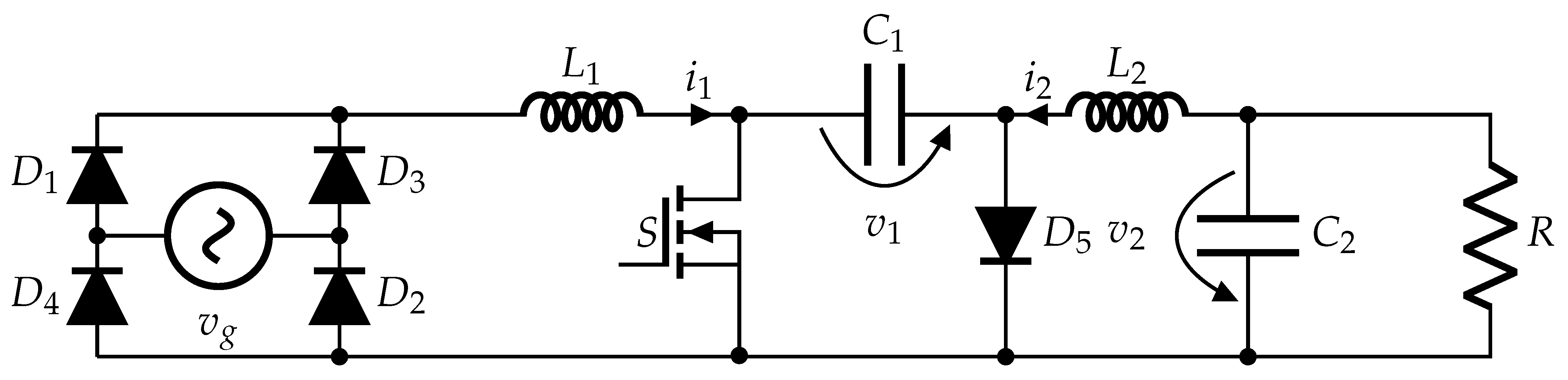
3.3. Buck-Boost Converter with PFC

In several applications, a voltage level lower than the input is required once a boost converter with PFC is used; therefore, an additional converter (buck converter) is employed. This topology combines the functionality of a buck converter and a boost converter into a single circuit. Some applications include consumer electronic devices, such as smartphones and computers, to adjust battery voltage. Also observed are applications in power amplification and control systems, where precise voltage regulation is required, as well as in power supplies that need to provide a variable voltage output. Figure 9 shows the classic structure of a buck-boost converter. By altering duty cycle of the switching transistor S, the output voltage can be changed. The energy stored in the inductance L is transferred using the diode D 5 to the capacitor C and the load R.
Although this converter circuit meets the request, it presents disadvantages in the efficiency of the entire feeder system given its high number of components. Consequently, in [42], the design and simulation evaluation of a single-phase bridgeless buck-boost converter that employs a switched capacitor configuration is presented. Under a load condition of 1 kW, an input voltage of 220 Vac and an output voltage of 200 V, a THDi of 4.22 % , and a PF at the input of 0.99 were obtained.
Another noteworthy work appears in [43] which proposes a circuit for a bridgeless buck-boost converter with a single-phase PFC. A continuos conduction mode is utilized for plant control design and modeling. Within the topology of this converter, a Zero Voltage Transition (ZVT) auxiliary circuit is introduced, the auxiliary switch is operated under current zero-crossing conditions, and the main switches are turned on and off under voltage zero-crossing conditions. Once the laboratory implementation is carried out for a nominal load of 500 W, the THD measurement equal to 2.7 % is obtained along with an efficiency of 97.3 % . The best power PF was 0.999 . An input voltage of 85 265 Vac and an output voltage equal to 96 Vdc were used for the PFC circuit.
Meanwhile, authors of [44] aim to improve energy consumption in the network when electric vehicle chargers are connected by proposing a two-staged battery charger consisting of a bridgeless buck-boost converter with interlaced single-phase PFC in the first stage (AC/DC). In the second stage, an LLC half-bridge converter is responsible for charging the battery. The first stage focuses on the THDi reduction and the high power factor. Using the two stages, a maximum efficiency of 92.8 % , a THDi level of 2.08 % , and a PF of 0.9994 were obtained in hardware for a load of 1 kW. The specifications for the first stage were an input voltage of 110 230 Vac and an output voltage of 55 Vdc.
In [45], a proposal for a buck-boost converter with PFC without a single-phase bridge and with a common ground between source and load is presented. This proposal eliminates the problems that the common mode current arise. The simulations carried out rendered a THDi of 3.7 % with a PF of 0.9993 , under a load scenario of 300 W, with 200 Vdc output, 110 Vac input, and a switching frequency of 80 kHz.
The elaboration of a single-phase boost-buck converter with active power decoupling through the Time-Sharing control strategy is carried out in [46]. The main features are the use of the PFC operation, active power decoupling, and constant control over the delivered direct voltage due to its inherent operation as a buck-boost. Once the circuit was modeled through the use of the Discontinuous Current Mode (DCM) and the Triangular Current Mode (TCM), using a grid voltage of 100 Vac, an output voltage of 200 Vdc, and a load power of 200 W, the following results were obtained:
  • MCD, experimental implementation: Operation under boost condition and active power decoupling were used, obtaining a THDi of 5.3 % , a FP of 0.99 and an efficiency of 90.2 % .
  • MCT, simulation implementation: Operation under boosting conditions and active power decoupling were also used, obtaining a THDi of 3.2 % , a FP of 0.99 and a higher efficiency than that obtained in MCD.
Considering that efficiency is one of the central axes to consider when using sources in final energy distribution systems, in [47], it is proposed to show the advantage of the topology of the versatile single-phase buck-boost converter, comparing it with the Single-Ended Primary Inductor Converter (SEPIC), topology displayed in Figure 10. The control strategy used is the typical internal current loop, particularly to obtain the current reference. A sinusoidal reference module that works with a Phase Locked Loop (PLL) is employed, but a voltage sensor is not employed. Both converters were designed and used in the study for an output voltage of 200 Vdc, an input voltage of 220 Vac, and a load power of 900 W. In the case of the buck-boost converter, an efficiency of at least 95 % was presented, and for the SEPIC converter, it was at least 88 % . These results were obtained by simulation.
Meanwhile, in [48], a comparison of different converter topologies with PFC was carried out, highlighting the main advantages and disadvantages of the application (battery charger). The developed control strategy aimed to find a controller that could operate on different duty cycle combinations to optimize efficiency while preserving sufficient voltage and current regulation (battery life), a high power factor, and a low THDi. The following experimental results were presented for a converter with a capacity of 1 kW, an input voltage of 80 to 400 Vac, and an output voltage of 140 Vdc: a power factor of 0.999 , a THDi of 4 % , and an efficiency of 93 % .
Finally, in [49], a battery charger for low-voltage electric vehicles is designed. This charger consists of two stages aiming to raise the power factor at the charger input as much as possible. The first stage consists of a buck-boost converter with a single switching element to decrease losses and improve efficiency. The second stage uses a flyback converter to involve galvanic isolation between the battery and feeder circuit. The control implementation was completed through code generated in the MATLAB/Simulink environment, which communicates with a 750 W experimental prototype to reduce control complexity. As a result, a power factor of 0.99 , a THDi of 1.6 % , and an efficiency of 95.12 % were measured. These results were given for a nominal input voltage between 160 and 250 Vac and an output voltage of 48 Vdc.
In the case of [50], a bidirectional three-phase rectifier with PFC and galvanic isolation is implemented. The control strategy for this rectifier is based on a space vector controller, where the components are optimized to predict the transformer current waveform. The transformer’s RMS current under partial load is significantly reduced compared with other modulation control methods. This type of control allows for a simpler control methodology for increasingly complex topologies. Thanks to this, a hardware validation was performed, obtaining a power factor of 0.996 , a THDi of 0.79 % , and an efficiency of 99.26 % for a circuit with 230 Vac input, 401 Vdc output, and a maximum power of 4.5 kW.
The flyback topology is essentially a buck-boost topology, which isolates the input and output using a transformer as a storage inductor. Figure 11 displays the basic flyback converter circuit, as can be seen by varying the transformer’s turns ratio the output voltage can be adjusted. Flyback is the simplest and most common isolated topology for low-power applications.
Regarding flyback topology, in [51], a circuit consisting of two flyback converters is analyzed. The energy controlled by both converters is distributed between the load and two DC link capacitors. The input voltage, together with the input current, remain in phase naturally because the AC-DC converter operates in discontinuous conduction mode. The DC-DC converter transfers the energy from the capacitors to the load in the next cycle. The first converter operates in discontinuous conduction mode to reduce switching losses and the second acts in critical conduction mode. To verify the operation of the proposed circuit, a 48 Vdc, and 100 W output prototype is built, an input of 100 240 Vac obtaining a PF of 0.993 with an efficiency of 91.39 % .
One of the main objectives of flyback converters is to eliminate the dead zone inherent to PFC. For this purpose, a Constant On-Time (COT) control strategy in Critical Conduction Mode (CRM) is commonly utilized. The main disadvantage of this control strategy is that the converter’s operating frequency varies considerably during a line power cycle, complicating the protection of power supplies with EMI filters. Therefore, the [52] study establishes a fixed switching frequency control (FFC) for a 120 W converter, with an input voltage of 90 to 264 Vac and an output voltage of 80 Vdc, leading to the following experimental results: PF of 0.975 , THDi of 1.44 % , and a maximum efficiency of 91.56 % .
Table 4 contains the results values reported by the works on the buck-boost converter with power factor correction. Some works worth highlighting are presented in [43,44,45,48] where a power factor equal to or greater than 0.999 is achieved. Alternative control proposals are also observed in [46,47,48], where some approaches are time-sharing control using triangular current mode and predictive digital current programmed control.

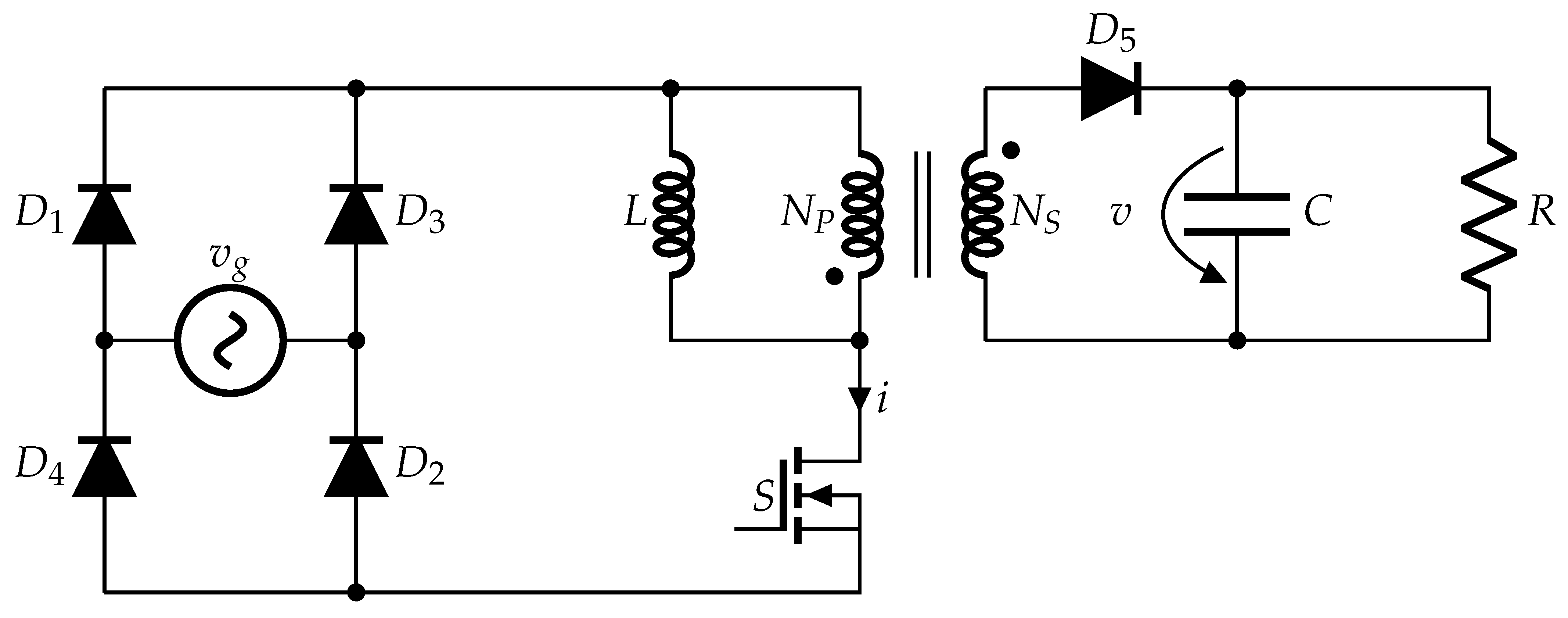
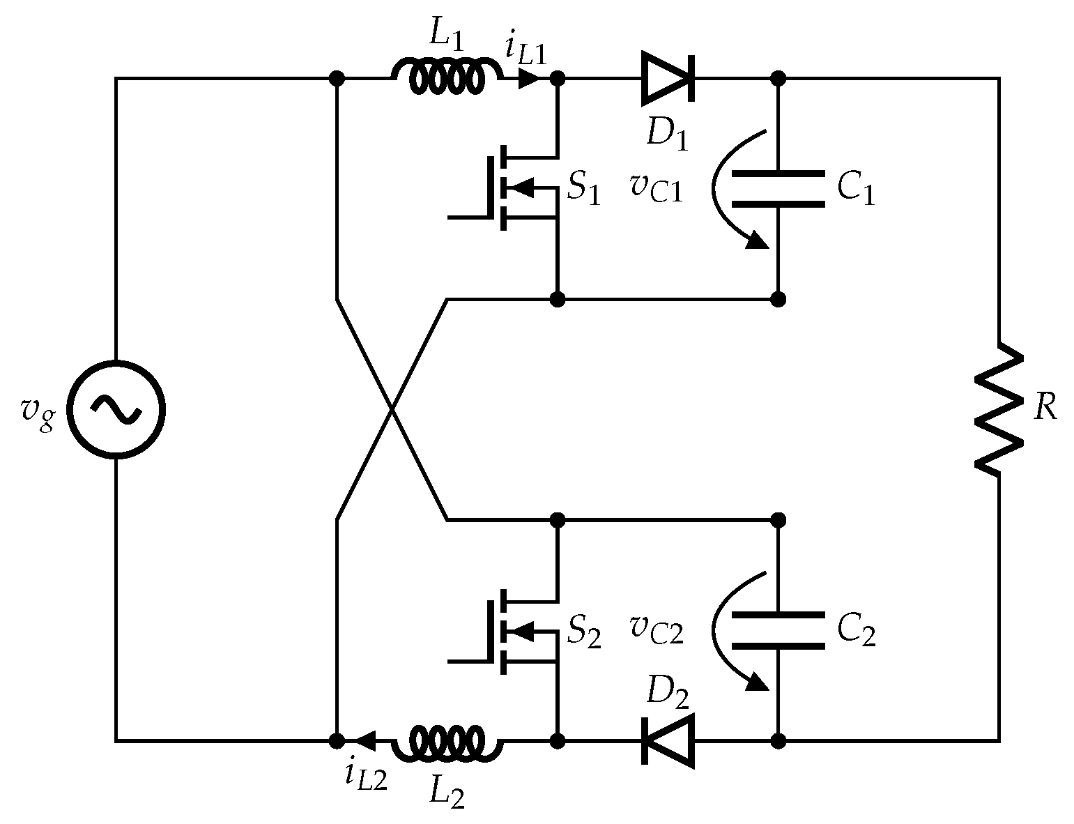
3.4. Cük Converter with PFC

The Cük converter is an efficient voltage converter with a DC voltage output that may be used as a voltage reducer and a voltage booster. This topology employs a capacitor instead of an inductor for energy storage and power transfer. The converter produces a ripple-free output and can be used in various applications such as motor drives and renewable energy, especially photovoltaic systems. The standard structure for a Cük converter circuit is presented in Figure 12. This topology utilizes two capacitors C 1 and C 2 , two inductances L 1 and L 2 ; the energy is driven to the load R using the the switch S and diode D 5 . Diodes D 1 to D 4 allow rectifying the voltage of the alternating source v g . Most of the papers reviewed in this section take this basic structure as a reference.
Regarding the extensive use of Brushless Direct Current Motors (BLDCM) in different appliances intended for residential use, in [53], a source together with its respective driver for a motor is designed and developed in simulation. The device employs a Cük converter with single-phase PFC, which has built-in inductances (transformer). For an input voltage of 90 270 Vac, a converter output voltage of 15 Vdc, an output power of 50 W, a THDi of 4.72 % , and a PF of 0.99 were obtained.
One advantage of the conventional single-phase Cük converter is that when acting in DCM, the PFC is automatic by simply using a voltage loop in the control design. This process causes the intermediate capacitor to suffer high stress due to the high voltage it must handle. To reduce this effect, this topology is modified by utilizing a variable inductance in [54]. The inductance variation occurs according to the transient values of the rectified input voltage. From there, a controlled polarization direct current is injected into the auxiliary winding of the variable inductance coil. In the hardware testing, a FP value greater than 0.997 , a THD value less than 5 % , and an efficiency value of up to 90.5 % were obtained. The above is given under an input voltage of 90 Vac, an output voltage of 72 Vdc, and a power consumption in the load of 108 W.
The input of undesirable signals into power supplies can lead to the deterioration of the components of the circuit along with their insulation. Hence, there are Electro-Magnetic Interference (EMI) filters to mitigate unwanted signals that may enter the source and even be reflected in the load. This type of filter is normally made of an LC circuit. In this way, in [55], the implementation of an LCL filter and the study of the performance of a single-phase isolated Cük converter with PFC is proposed considering the use of this filter. The modeling and control were carried out including isolated cases of small and large signals. All this can be done with the use of a PI controller. The parameters of the plant implemented in hardware included an input voltage of 140 Vac, an output voltage of 25.9 Vdc, and a power in the load of 50 W. The measurements obtained were THD of 4.83 % , a PF of 0.998 , and an efficiency of 85 % (for the LCL filter).
As displayed in Section 3.1, in [23] a simulation comparison was made between the boost converter, Cük, and Zeta (single-phase). The THD level was evaluated under load variation and continuous mode during the current operation (results were reported in Section 3.1).
A bridgeless Cük converter with PFC is described and analyzed in [56]. To reduce the size of the components that conform the converter circuit, soft switching is used since it increases the frequency without compromising the converter efficiency. The presence of an input inductor avoids the implementation of an input filter. The validation of the results is given by means of a 200 W hardware prototype, with an input voltage of 110 Vac and an output voltage of 80 Vdc achieving the following performances: a power factor of 0.998 , a THDi of 5.85 % and an efficiency of 96 % .
Finally, a control methodology that uses a current sensor for a switched reluctance motor drive while ensuring the supply power quality is presented in [57]. The study is focused on low-power loads, such as household appliances and industrial applications. The Cük converter is located between the voltage input and the drive to reduce the THDi. The nominal power is 500 W, with an input and output voltage of 220 Vac and 100 to 300 Vdc, respectively. The control method is operated (evaluated) estimating the rotor position through data tables, which reduces memory usage and controller complexity. The results were extracted from an experimental prototype where the following measurements were obtained for the first PFC stage: power factor between 0.99 and 1.0 and THDi 3.8 % .
The summary of the results reported in the papers is presented in Table 5. In this group of works, voltage loop and current loop control are observed again. Among the works carried out, it is worth highlighting a Cük converter using a variable inductor that varies with the transiently rectified input voltage to improve the power factor. It is also worth noting that power factors close to 0.998 are achieved, and different output power and voltage values are considered.

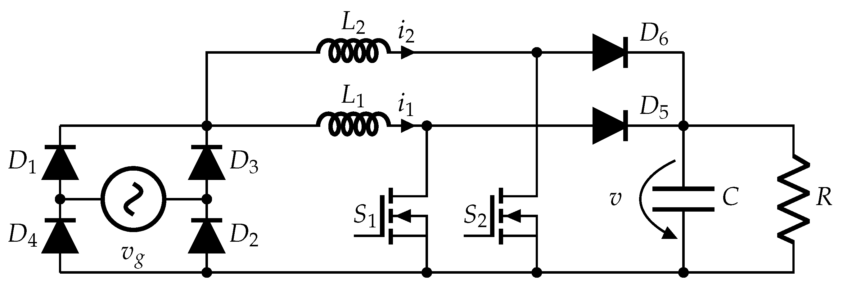
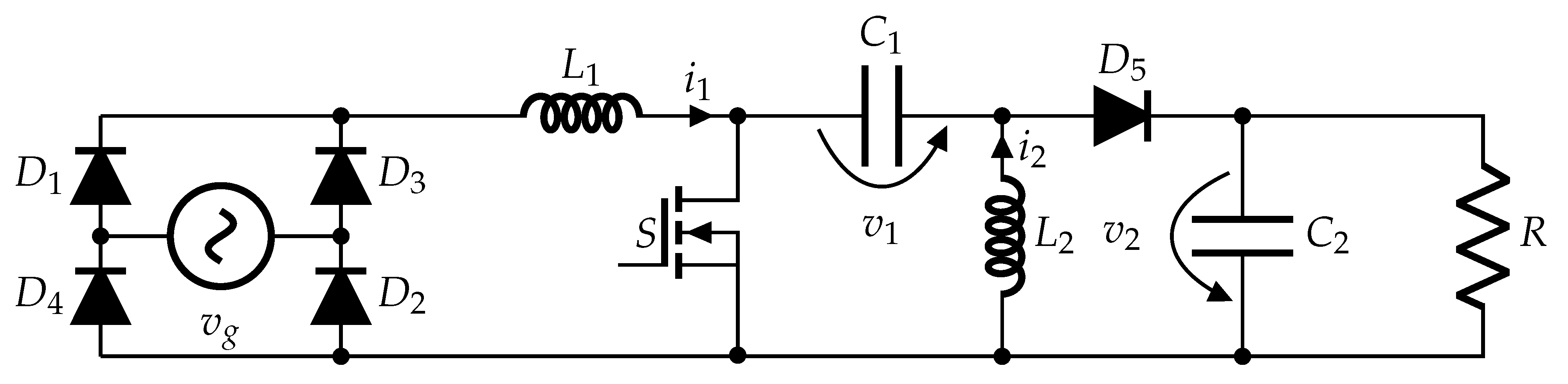
3.5. Dual Boost Converter with PFC

The dual-boost interleaved converter topology with single-phase PFC is relatively new. The double dual boost converter offers high efficiency in energy conversion, with a higher output voltage increase and reduced input current ripple compared to a classic boost converter topology. Applications requiring high voltage increase and effective energy management, such as solar systems, electric cars, and other renewable energy systems are particularly well-suited for this converter. This topology eliminates ripple by connecting two boost converters in an antiparallel fashion, as displayed in Figure 13. This approach employs two symmetrical branches (crusades) formed by two inductances L 1 and L 2 , two capacitances C 1 and C 2 , and the switching elements S 1 and S 2 and the respective diodes D 1 and D 2 that allow the energy to be directed to the load R. In this case, the alternating voltage source v g is connected directly to the converter branches.
Authors in [58] tested the configuration of dual boost converters. One novelty consists of the sum of capacitances, which provides three separate output voltage levels that operate interleaved at the input (depending on the switching stages). The laboratory tests were performed where the best efficiency value obtained was 95.8 % for a load of 200 W and an input voltage of 130 Vac. Other results were measured for an output voltage at the load of 350 Vdc and a maximum power consumption of 550 W. In such a scenario, the following measurements were obtained:
  • Using a input voltage of 90 V c a : THD equal to 0.5 % , FP of 0.996 , and an efficiency of 92.05 % .
  • Using a input voltage of 110 V c a : THD equal to 0.84 % , FP of 0.99 , and an efficiency of 93.7 % .
  • Using a input voltage of 130 V c a : THD equal to 1.7 % , FP of 0.986 , and an efficiency of 94.6 % .
Among the issues associated with delivering adequate energy to the final consumer appears the ripple of the output voltage, which is one of the most significant. In most cases, the simplest solution is to connect a large capacitor in parallel, usually electrolytic. This implies a higher cost and increased risk due to discharge currents from the capacitor. Consequently, in [59], a bridgeless converter with PFC is designed and implemented to replace the capacitor. This is based on a power decoupling and consists of two stages: the first is a double boost converter without bridge and PFC, and the second stage has a converter with bidirectional buck-boost power decoupling. In the simulation, a PF greater than 0.999 was obtained with an input voltage equal to 220 Vac, an output voltage of 400 Vdc, an output power of 210 W, and a switching frequency of 100 kHz and 50 kHz for the first and second stages, respectively.
Under the traditional approach, in [60], the design and innovation of drivers is oriented towards the supply of one of the most common loads, namely, the luminaries. In this case, a driver for an LED lamp was implemented, consisting of a double boost converter with PFC (first stage) and an LLC half-bridge resonant converter (second stage). In the measurement of the plant mounted in the laboratory, a PF of 0.9879 , a THD of 5.7951 % , and an efficiency of 89.85 % were obtained. The results were obtained with an input voltage of 110 Vac, an output voltage of 36 Vdc, nominal power consumption of the luminaire of 100 W, and a switching frequency of 100 kHz.
Regarding comparisons of papers on dual boost converters with power factor correction, Table 6 shows the identified papers with their main features. Reference [58] highlights a hardware implementation with the lowest THDi. It is worth highlighting reference [59] as it exhibits the highest power factor (0.999 reported). Finally, a typical implementation of a PI controller for voltage loop and current loop is utilized in [58]. Other control approaches are average current control and high-voltage resonant control.

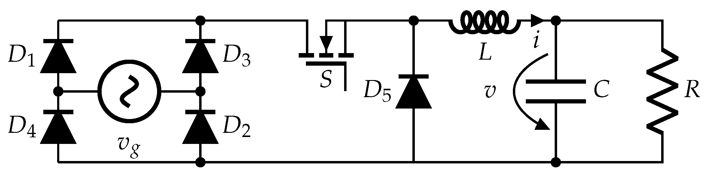
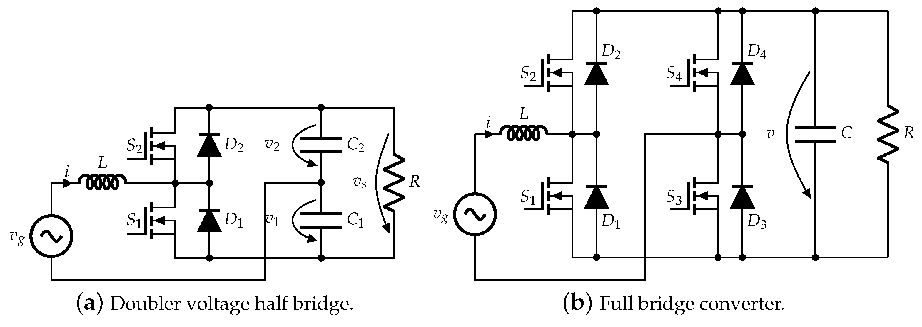
3.6. Totem Pole Bridgeless Converter with PFC

Totem-pole topology integrates the rectification and boost stages and uses two switching branches that operate at different frequencies. This topology generally offers better performance than interleaved boost converters; however, the additional active switches make the control circuitry more complex. This type of converter is the most common application for charging electric vehicles. A bare totem pole bridgeless converter circuit is displayed in Figure 14; since the two switches, S 1 and S 2 , are positioned vertically, this topology is known as totem-pole. Switches can be used in place of the line rectification diodes D 1 and D 2 to increase efficiency. Different strategies are proposed to deliver the energy to load R focused on power factor correction.
Variants of this topology can be seen in Figure 15, where there is a half-bridge converter in Figure 15a and a full-bridge converter in Figure 15b. The doubler voltage half-bridge topology (Figure 15a) presents a simple conversion circuit with fewer switches. Its main advantage is high efficiency, since at any given time, there is only one voltage drop, which is produced by the semiconductor that is on. On the other hand, the full-bridge topology (Figure 15b) is widely used in high-power applications since it allows efficient and symmetrical energy conversion, supporting high current levels with lower conduction losses per branch.
In [61], the goal is robustness, control simplification, and efficiency in converters. For this reason, a Totem Pole interleaved converter with PFC is proposed, which uses only two voltage sensors; that is, there is no current control loop since the current naturally follows the input voltage, obtaining a PF close to unity. For this research, an input voltage of 127 Vac, an output voltage of 400 Vdc, an output power of 1 kW, and a switching frequency range of 40 200 kHz were used obtaining the following results:
  • Power Factor: 0.998 .
  • Total Harmonic Distortion: 6.14 % .
  • Efficiency: 97.51 % .
In addition, charging electric vehicles is also an application considered for this converter topology. Thus, a Totem Pole hybrid converter that uses a switched capacitor cell capable of delivering a voltage lower than the input voltage is proposed in [62]. The purpose is to avoid the issues that normally occur in classic PFC topologies since an extra stage must be implemented in the latter to reduce voltage, increase the number of components, and decrease the overall converter efficiency. Once the assembly was completed, the following results were obtained: THD of 2.19 % and a PF of 0.9998 . These results were given with an input voltage equal to 270 Vac, an output voltage of 400 Vdc, and a nominal power of 1 kW.
Due to the high demands on energy efficiency in recent decades, regardless of the load variation that can be connected to a source, in [63], a Totem Pole converter topology with PFC using IGBT’s and SiC (Silicon Carbide) diodes is proposed. A maximum efficiency of 99 % was obtained with an output power of approximately 1.6 kW and a switching frequency of 65 kHz with the plant implemented in a laboratory.
Meanwhile, in [64], a Totem Pole converter with PFC is implemented in the laboratory to evaluate the performance of a new control strategy. This consists of an interleaved digital control method for GaN (Gallium Nitride)-based switching devices. The converter operates in Critical Conduction Mode (CCM), and the behavior of the implemented PLL control is analyzed. In addition to suggesting a technique for the digital implementation of interleaved CrM PFC converters, this investigation aims to determine the connection between phase error and compensation. The implemented plant has an input voltage of 220 Vac, an output voltage of 400 Vdc, and a nominal power of 3.6 kW.
Another approach to manufacturing converters is to reduce power losses by optimizing components. Based on the above, in [65], the Pareto algorithm technique is employed to design the inductors in a bridgeless totem-pole boost converter with PFC. This approach aims to reduce the occupied volume of the coils while also projecting to maintain the lowest possible losses, thus offering a point in favor of the competition of power supply systems for electric vehicles with On-Board Chargers (OBC). The experimental implementation established an input voltage of 220 Vac, an output voltage equal to 650 Vdc, a nominal converter output power of 3.3 kW, and a switching frequency of 70 kHz. An efficiency of 98.14 % was measured for the previous plant parameters.
In [66], authors also focus on adequately designing chargers for electric vehicles to reduce THD. Different controllers are implemented in the simulation for a totem pole boost converter without a bridge and with PFC. These are Proportional-Integral (PI) controller, Proportional-Resonant (PR) controller, Fractional Proportional-Integral-Derivative (FOPID) controller, and an Artificial Neural Network (ANN). The plant has an input voltage of 230 Vac, an output voltage of 400 Vdc, a nominal power of 3.3 kW, and a switching frequency of 65 kHz, where a minimum THD of 3.86 % was finally obtained for the case of the FOPID and ANN controllers.
Regarding the motivation to develop chargers for electric vehicles, in [67] a charging infrastructure (G2V, Grid to Vehicle) is proposed employing an on-board charger consisting of a totem pole converter in MCC and with PFC. For the G2V charging mode, an input voltage of 230 Vac, an output voltage of 400 Vdc, an output power equal to 7.7 kW, and a switching frequency of 65 kHz were considered. For these conditions, a THD value equal to 4.81 % and an efficiency of 98.38 % were obtained in simulation.
The use of coupled inductors can be beneficial for totem pole converters with PFC since it helps solve problems related to THD, losses, current ripple, and power density. Therefore, in [68], this circuit was implemented using a Proportion Integral Resonant (PIR) control strategy to reduce the problem of zero-crossing distortion. The parameters of the converter assembled are an input voltage of 220 Vac, an output voltage of 390 Vdc, a nominal output power of 7.7 kW, and a switching frequency of 50 kHz. For this plant, a THD of 1.87 % , a PF of 0.9989 , and a maximum efficiency of 99.07 % were measured.
The work presented in [69] seeks to model and control a power converter-based power supply system that uses the electrical grid to power electromagnetic contactors. The study focuses on minimizing the consequences of voltage drops across the contacts and reducing their vibrations. At the same time, the objective is to reduce the impact of the contactors on the quality of power delivered by the grid to obtain a high power factor. This is achieved through a Totem Pole converter with PFC, a step-down converter stabilizing the voltage the contactors consume. This system has a nominal power of 500 W, an input voltage of 230 Vac, and an output voltage between 350 and 400 Vdc. Under the hardware implementation of a prototype, the measurements obtained a power factor of 0.98 and an efficiency of 97 % .
Meanwhile, in [70], the objective is to minimize the fluctuations in the output voltage and the distortion of the bridgeless totem pole converter with PFC that charges an electric vehicle as it is possible. A control approach based on a fuzzy logic controller and the active rejection theory is established to achieve a high power factor. This controller can perform a self-adaptive adjustment. The feasibility of this control is evaluated through the experimental implementation of 3 kW, an input voltage of 220 Vac and an output voltage between 320 and 650 Vdc, where the following results were obtained: THDi of 1.66 % and an efficiency greater than 95 % .
For the case considered in [71], the design of an external charger for electric vehicles (charging stations) is proposed. This charger comprises a compact totem pole converter model with open-loop control dynamics. This converter has a nominal power of 60 W, an input voltage of 12 Vac, and an output voltage of 25 Vdc. The main evaluation components are the power factor, efficiency, and, therefore, the converter losses. Although there was a hardware implementation, the authors do not display the experimental results. Therefore, the simulation results obtained are a power factor of 0.912 , a THDi of 32.6 % , and an efficiency of 94 % .
In the research [72], a converter is designed to power and optimize the operation of a permanent magnet brushless DC motor. The converter is controlled by high-resolution pulse width modulation. The control strategy used to regulate the output voltage is based on fuzzy logic through adaptive control. The regulated voltage output is passed to a VSI inverter to power the motor. The application of this control methodology for the PFC converter was verified through hardware implementation with a Spartan 6E FPGA. A THDi equal to 1.6 % and a maximum efficiency of 97 % were measured. An experimental design of 170 230 Vac input and an output voltage of 300 Vdc were used for the tests.
Table 7 shows the research comparison regarding totem pole bridgeless converters with power factor correction. In this regard, it highlights the work of [68], where the greatest efficiency is obtained for a plant with hardware implementation (equal to 99.07 % ). It is also worth considering the paper [62] where the highest power factor (reporter 0.9998 ) is obtained for hardware implementation. Finally, classical implementations of PI controllers for voltage loop and current loop are displayed in [66,67,70,72]. Some nonlinear control strategies observed are artificial neural networks, fuzzy logic, and zero-crossing distortion inhibitory strategies.

4. Discussion

This review shows different topologies depending on the needs for energy conversion. It is identified that certain topologies that achieve high power factor values require additional elements, thus increasing costs. In this regard, the question arises as to whether the increase in the cost of conversion systems with power factor correction compensates for the cost of reducing reactive power. This is an aspect that must be considered for consumers and generators. The ideal design consists of obtaining converters with a high power factor and low cost.
Figure 16 shows that two study approaches were identified within the designs and topologies reviewed. The first approach is to maintain the power factor as close to unity as possible, reducing the reactive currents seen by the grid. This is achieved through different control strategies. The second approach focuses on the power losses that the circuit may have. Most of these losses occur in the switching devices (IGBTs/MOSFETs), the converter copper, and the resistances of the capacitors and inductors. This last approach seeks to modify the circuit through topology hybridization and circuit mutation.
Wide-bandgap semiconductors based on silicon carbide (SiC) and gallium nitride (GaN) have revolutionized the design of PFC converters, providing faster switching, lower losses, and greater thermal tolerance compared to traditional semiconductors. These properties allow for higher efficiency levels, significantly reduced passive and heatsink sizes, and more compact and lightweight designs. Although SiC and GaN devices may have a higher initial cost, their energy efficiency, power density, and reduced long-term total system cost benefits make them an increasingly viable and attractive option for demanding power electronics applications.
Regarding the advancement in power converter technology, reference [73] displays an exhaustive review of the electrical characteristics of the latest commercial power devices based on wide bandgap materials. Likewise, authors of this reference investigated and compared the static and dynamic behavior of commercial power switching devices to design power electronics converters, taking full advantage of the benefits of wide bandgap power devices. On the other hand, regarding control techniques, in [74], a PLL is proposed not only to estimate the angle of the electrical network and generate the instantaneous reference current but also to reject the noise around the zero crossings, which is implemented in Texas Instruments microcontrollers of the C2000 family. It is also worth noting the work of [75] where an approach is proposed to select an optimal location and the tuning of control variables by identifying the worst-case contingencies for the recently proposed Interline Direct Current Power Flow Controller (IDC-PFC) in MultiTerminal High-Voltage DC (MT-HVDC) networks, based on the maximum flow-min cut theory. The objective is to optimize the placement of PFCs to maximize the transmission capacities of the network.
Table 8 shows a comparison of different converters identified in the review. Aspects such as efficiency, complexity, applications, and some notes are considered. As can be seen, several specific converter topologies identified in the review are also included; besides, different converter alternatives depend on the application and requirements for power, efficiency, and ease of implementation.
As electronic applications become more compact and efficient, power converters with power factor correction face technological challenges that require innovative solutions, especially in electromagnetic interference mitigation, high-frequency magnetics management, and control strategies. Switching converters generate electromagnetic noise that can affect other devices. Considerations such as compact EMI filters, modulation techniques, and precise identification of interference sources are all worth investigating. On the other hand, increasing the operating frequency of converters reduces the size of passive components. However, hysteresis losses, eddy currents, and other nonlinear effects in magnetic cores are significant at high frequencies. In this regard, research can be conducted into modeling techniques that allow for accurate prediction of magnetic behavior under dynamic switching conditions. Research can also be done into resonant topologies that take advantage of soft switching characteristics to reduce stress on the magnetic components; however, this increases the complexity of design and control.
Control strategies used in PFC converters have evolved significantly, ranging from classical methods such as proportional-integral control, characterized by its simplicity and effectiveness under linear conditions, to advanced approaches such as sliding-mode control, which offers high robustness to disturbances and parameter variations. On the other hand, predictive control allows for anticipating system behavior, optimizing dynamic response, and reducing settling time. More recently, controllers based on neural networks and artificial intelligence have gained prominence due to their adaptive and learning capabilities, allowing them to improve system efficiency and stability in highly variable and nonlinear environments. Since digital control offers significant flexibility in the design of control strategies, research areas may be focused on developing robust algorithms to face grid disturbances (voltage drops, harmonics, and imbalances). Also, research can be done on implementing adaptive and predictive controls that address load or grid variations (smart grid approach).
As this review has shown, PFC converters are essential for improving energy efficiency and reducing harmonic distortion in power conversion systems. However, hardware implementation presents significant challenges, such as the design of robust controllers to load and line variations, the power dissipation of components due to conduction and switching losses, and the appropriate selection of semiconductor devices and other circuit elements. These demands increase implementation costs, as high-quality components and complex control systems are required. Despite these challenges, real-world testing has shown that PFC converters substantially improve power quality, standards compliance, and overall system efficiency.
Different converter topologies with PFC are selected based on the specific requirements of each application. For example, in electric vehicle charging, interleaved boost, doubler voltage half-bridge, or full-bridge topologies are preferred due to their high efficiency and ability to handle high power. In LED drivers, where low power consumption and good current regulation are required, flyback or buck-boost topologies with integrated PFC are used, optimizing size and cost. For energy harvesting, where available power is limited and variable, high-efficiency converters such as boost converters with Maximum Power Point Tracking (MPPT) techniques are utilized, ensuring optimal use of the captured energy.
Finally, converters with enhanced PFCs contribute significantly to energy savings by optimizing average power use and increasing the distortion factor, thereby improving grid utilization. By maintaining a power factor close to unity, these converters reduce unnecessary current demand on the electrical grid, thereby reducing transmission and distribution losses. This efficiency is reflected in lower operating costs and a reduction in overall energy consumption and, consequently, in emissions associated with power generation. Together, these technological advances support sustainability and help mitigate the environmental impact of modern electronic systems.

5. Conclusions

The study of converters with high power factor is a relevant aspect of energy efficiency. For this, different topologies are identified according to the applications to increase or reduce voltage. This review shows that not all the works report the same metrics, making the comparisons highly complex. However, it is worth highlighting the intention behind the research into power converters with power factor correction as an essential aspect of electrical energy quality.
Among the studies presented, a design trend was identified for battery chargers to power various electric transportation vehicles at low voltage. Another recurring application is the use of converters for photovoltaic sources. It is interesting to identify whether there are significant performance changes in converter topologies depending on their application in different types of renewable energy, thus optimizing the use of power electronics for power generation projects.
Regarding the general observations from the review, it is clear that the dominant controller in the different studies carried out is the PI controller. The topology with the highest average PF is the Totem Pole Bridgeless Converter. Meanwhile, the topology with the highest THDi is the Buck Converter. Except for [65], none of the studies exceeds 450 V output. It is also observed that most of the work carried out is for the boost converter with power factor correction.
Digital control (using boards) predominates within control approaches due to its versatility in implementing different programming strategies. Furthermore, an increasing number of studies are opting to use more than one converter topology within power conversion sources to adapt to the problems of EMI, supply voltage fluctuations, overloads, and switching device losses. In the latter, the reviewed research did not pay considerable attention to materials studies, instead preferring to design circuits that reduce the number of switches. The most common materials found in the review were the classic silicon (Si) and germanium (Ge), and some gallium arsenide (GaAs).
The review shows that different topologies achieve a power factor of 0.99 ; however, certain topologies require additional elements, increasing costs. Research is also being carried out on control strategies for achieving high power factors in addition to the topologies of the conversion circuits.
Several alternatives exist for research to improve energy conversion circuits using conventional techniques such as PI controllers or novel controllers using artificial intelligence techniques such as neural networks or reinforcement learning algorithms. Research fields may concentrate on creating reliable algorithms to deal with grid disturbances (voltage drops, harmonics, and imbalances) since digital control provides a flexibility in the design of control techniques. Additionally, studies on applying predictive and adaptive controls that can handle load or grid fluctuations can be conducted.
Research in this field could focus on developing hybrid topologies that integrate conventional configurations with resonant structures to optimize efficiency and minimize switching losses. Another promising research direction is the integration of these converters with smart grid technologies to support advanced energy management schemes, including demand response and load balancing. Finally, future studies could explore incorporating sustainable design approaches to reduce environmental impact.
Finally, this review paper is intended to serve as a reference for designing, simulating, and implementing power converters with new control strategies that allow for high power factors and improved power quality.

Author Contributions

Conceptualization, A.Q., J.B. and H.E.; Methodology, A.Q., J.B. and H.E.; Project administration, A.Q., J.B. and H.E.; Supervision, H.E.; Validation, A.Q.; Writing—original draft, A.Q., J.B. and H.E.; Writing—review & editing, A.Q., J.B. and H.E. All authors have read and agreed to the published version of the manuscript.

Funding

This research received no external funding.

Institutional Review Board Statement

Not applicable.

Informed Consent Statement

Not applicable.

Data Availability Statement

Not applicable.

Acknowledgments

The authors express gratitude to the Universidad Distrital Francisco José de Caldas.

Conflicts of Interest

The authors declare no conflict of interest.

References

  1. Krishna, L. Automatic Power Factor Correction Using Arduino Micro Controller; Archers & Elevators Publishing House: Bangalore, India, 2023. [Google Scholar]
  2. Noh, M.A.M.; RodhiSahid, M.; Duraikannan, S. Implementation of A New Single-Stage Bridgeless Boost Half-Bridge AC/DC Converter with Bidirectional Switch. Turk. J. Comput. Math. Educ. 2021, 12, 1331–1341. Available online: https://turcomat.org/index.php/turkbilmat/article/view/4394 (accessed on 4 June 2024).
  3. Bayona, J.; Guarnizo, J.; Gelves, N. Pulse Width Prediction Control Technique Applied to a Half-Bridge Boost. Tecciencia 2018, 13, 47–54. [Google Scholar] [CrossRef]
  4. Lo, Y.-K.; Ho, C.-T.; Wang, J.-M. Elimination of the Output Voltage Imbalance in a Half-Bridge Boost Rectifier. IEEE Trans. Power Electron. 2007, 22, 1352–1360. [Google Scholar] [CrossRef]
  5. Jiang, S.; Cao, D.; Li, Y.; Peng, F.Z. Grid-Connected Boost-Half-Bridge Photovoltaic Micro Inverter System Using Repetitive Current Control and Maximum Power Point Tracking. IEEE Trans. Power Electron. 2012, 27, 4711–4722. [Google Scholar] [CrossRef]
  6. Vinnikov, D.; Chub, A.; Liivik, E.; Blaabjerg, F.; Siwakoti, Y. Boost Half-Bridge DC-DC Converter with Reconfigurable Rectifier for Ultra-Wide Input Voltage Range Applications. In Proceedings of the IEEE Applied Power Electronics Conference and Exposition (APEC), San Antonio, TX, USA, 4–8 March 2018. [Google Scholar] [CrossRef]
  7. Le, T.T.; Lee, J.; Choi, S. Single-Stage Totem-Pole AC-DC Converter Based on Boost Half-Bridge Structure for Battery Chargers. IEEE Trans. Power Electron. 2024, 39, 1060–1073. [Google Scholar] [CrossRef]
  8. Singh, A.; Tiwari, A.N. Analysis of Bridge and Bridgeless type PFC AC-DC Boost Converter. In Proceedings of the International Conference on Electrical Engineering (ICE3), Gorakhpur, India, 14–15 February 2020. [Google Scholar] [CrossRef]
  9. Makkapati, S.; Ramalingam, S. Comparative Analysis of Different Single Stage PFC Integrated Half Bridge LLC converter for LED Lighting. In Proceedings of the International Conference on Electrical Engineering (ICPECTS), Chennai, India, 8–9 December 2022. [Google Scholar] [CrossRef]
  10. Tamayo, M.T. El Proceso de la Investigación Científica, 5th ed.; Limusa: México City, México, 2011. [Google Scholar]
  11. Creswell, J.W. RESEARH DESIGN, Qualitative, Quantitative, and Mixed Methods Approachs, 4th ed.; SAGE Publications: Los Angeles, CA, USA; London, UK; New Delhi, India; Singapore; Washington, DC, USA, 2014. [Google Scholar]
  12. Liberati, A.; Altman, D.G.; Tetzlaff, J.; Mulrow, C.; Gøtzsche, P.C.; Ioannidis, J.P.; Clarke, M.; Devereaux, P.J.; Kleijnen, J.; Moher, D. The PRISMA statement for reporting systematic reviews and meta-analyses of studies that evaluate health care interventions: Explanation and elaboration. PLoS Med. 2009, 6, 339. [Google Scholar] [CrossRef]
  13. Urrutia, G.; Bonfill, X. Declaración PRISMA: Una propuesta para mejorar la publicación de revisiones sistematicas y metaanálisis. Med. ClÍnica 2010, 135, 507–511. [Google Scholar] [CrossRef]
  14. Campos, H.; Soares, J.; Badin, A.; Cortez, D. Single-Phase Hybrid Switched-Capacitor PFC Boost Rectifier with Low Voltage Gain. IEEE Trans. Power Electron. 2023, 38, 968–976. [Google Scholar] [CrossRef]
  15. Akhmetov, Z.; Abdelraziq, M.; Pantic, Z. Low Conducted-EMI Single-Phase Boost PFC with Sliding Frequency Modulation. In Proceedings of the IEEE Applied Power Electronics Conference and Exposition (APEC), Orlando, FL, USA, 19–23 March 2023; pp. 1784–1789. [Google Scholar] [CrossRef]
  16. Li, J.; Yan, T.S.; Feng, C.Y.; Yue, H. Flicker-Free LED Driver Based on Tapped Inductor Boost-Flyback PFC Converter. In Proceedings of the Panda Forum on Power and Energy (PandaFPE), Chengdu, China, 27–30 April 2023; pp. 538–543. [Google Scholar] [CrossRef]
  17. Kumar, S.; Kumar, N. A Boost PFC fed LLC Resonant Converter for Electric Vehicle Application. In Proceedings of the International Conference on Power, Instrumentation, Control and Computing (PICC), Thrissur, India, 19–21 April 2023; pp. 1–5. [Google Scholar] [CrossRef]
  18. Kranda, E.; Gokdag, M.; Gulbudak, O.; Prabaharan, N. Enhancement of Steady-State Performance of PFC Boost Rectifier using Modulated Model Predictive Control. In Proceedings of the 5th Global Power, Energy and Communication Conference (IEEE GPECOM), Nevsehir, Turkiye, 14–16 June 2023; pp. 50–55. [Google Scholar] [CrossRef]
  19. Kumar, G.; Chenchireddy, K.; Begum, T.; Aniketh, M.; Kumar, P.; Sayeed, Z. Design and Simulation of Interleaved Boost PFC Converter with PR Controller. In Proceedings of the International Conference on Sustainable Communication Networks and Application (ICSCNA), Theni, India, 15–17 November 2023; pp. 778–782. [Google Scholar] [CrossRef]
  20. Lu, S.; Ma, H.; Zhang, T.; Tang, L.; Chen, Z. A Novel Boost PFC Converter with Inherent Boundary Conduction Mode Operation. In Proceedings of the IEEE 4th China International Youth Conference On Electrical Engineering (CIYCEE), Chengdu, China, 8–10 December 2023; pp. 1304–1308. [Google Scholar] [CrossRef]
  21. Correia, W.B.; Júnior, D.O.d.; Vasconce, F.J.d.S.; Medeiros, J.W. Improvements on PFC boost self-control structure. In Proceedings of the IEEE 8th Southern Power Electronics Conference (SPEC), Florianopolis, Brazil, 26–29 November 2023; pp. 1–5. [Google Scholar] [CrossRef]
  22. de Melo, I.D.F.; Teixeira, G.A.; Barbosa, E.A.O.; Neto, R.C.; Bradaschia, F.; Neves, F.A.S. Comparison Analysis of Current Controllers Applied to a Boost Power Factor Correction Converter. In Proceedings of the IEEE 8th Southern Power Electronics Conference (SPEC), Florianopolis, Brazil, 26–29 November 2023; pp. 1–6. [Google Scholar] [CrossRef]
  23. Purohit, R.; Bhalla, V. Comparative Analysis of Boost, Cuk and Zeta PFC Converters in Continuous Current Mode. In Proceedings of the 9th IEEE India International Conference on Power Electronics (IICPE), Sonipat, India, 28–30 November 2023; pp. 1–6. [Google Scholar] [CrossRef]
  24. Ramos, C.; Saavedra, A.; Bastidas, J. Co-Design of the Control and Power Stages of a Boost-Based Rectifier with Power Factor Correction Depending on Performance Criteria. Computation 2022, 10, 61. [Google Scholar] [CrossRef]
  25. Okilly, A.H.; Baek, J. Design and Fabrication of an Isolated Two-Stage AC-DC Power Supply with a 99.50% PF and ZVS for High-Power Density Industrial Applications. Electronics 2022, 11, 1898. [Google Scholar] [CrossRef]
  26. Zhang, R.; Dong, J.; Wang, L.; Ma, W.; Yin, G. Stabilizing the Boost PFC Converter with a Time Delay Feedback Controller. Electronics 2023, 12, 2291. [Google Scholar] [CrossRef]
  27. Han, J.-K. Frequency Modulation Scheme for CCM Boost PFC Converter to Improve THDinLight-Load Condition. Electronics 2024, 13, 256. [Google Scholar] [CrossRef]
  28. Tayar, T.; Abramovitz, A.; Shmilovitz, D. DCM Boost PFC for High Brightness LED Driver Applications. Energies 2021, 14, 5486. [Google Scholar] [CrossRef]
  29. Liu, X.; Zhang, D.; Wang, W.; Zhang, F.; Yuan, J.; Liu, N. Adaptive Charge-Compensation-Based Variable On-Time Control to Improve Input Current Distortion for CRM Boost PFC Converter. Energies 2022, 15, 4021. [Google Scholar] [CrossRef]
  30. Ortiz-Castrillón, J.R.; Saldarriaga-Zuluaga, S.D.; noz-Galeano, N.M.; López-Lezama, J.M.; Benavides-Córdoba, S.; Cano-Quintero, J.B. Optimal Sliding-Mode Control of Semi-Bridgeless Boost Converters Considering Power Factor Corrections. Energies 2023, 16, 6282. [Google Scholar] [CrossRef]
  31. Han, J.-K. Efficiency and PF Improving Techniques with a Digital Control for Totem-Pole Bridgeless CRM Boost PFC Converters. Energies 2024, 17, 369. [Google Scholar] [CrossRef]
  32. Cheng, C.-A.; Cheng, H.-L.; Chang, C.-H.; Chang, E.-C.; Tsai, C.-Y.; Lan, L.-F. A Novel and Cost-Effective Drive Circuit for Supplying a Piezoelectric Ceramic Actuator with Power-Factor-Correction and Soft-Switching Features. Micromachines 2021, 12, 1229. [Google Scholar] [CrossRef]
  33. Kishore, G.I.; Tripathi, R.K. Single-phase unidirectional AC-DC PFC converter with switched capacitors. Int. J. Electron. 2021, 108, 305–321. [Google Scholar] [CrossRef]
  34. Fusic, J.; Shunmathi, M.; Sitharthan, R.; OV, G.S.; Ramesh, H.; Kumar, A. Efficient power factor correction in single phase AC-DC boost converter for retrofitted electric bicycle battery charging: A finite element analysis approach. Comput. Electr. Eng. 2024, 119, 109549. [Google Scholar] [CrossRef]
  35. Li, G.; Huang, H.; Song, S.; Liu, B. A nonlinear control scheme based on input-output linearized method achieving PFC and robust constant voltage output for boost converters. Energy Rep. 2021, 7, 5386–5393. [Google Scholar] [CrossRef]
  36. Ganesh, R.J.; Kodeeswaran, S.; Kavitha, M.; Ramkumar, T. Performance analysis of piezoelectric energy harvesting system employing bridgeless power factor correction boost rectifier. Mater. Today Proc. 2021, 45, 486–494. [Google Scholar] [CrossRef]
  37. Chen, Z.; Liu, Y.; Dong, Z.; Feng, K.; Liu, C. A True Bridgeless Buck-Type PFC Converters with Low Total Harmonics Distortion. In Proceedings of the 49th Annual Conference of the IEEE Industrial Electronics Society (IECON), Singapore, 16–19 October 2023; pp. 1–6. [Google Scholar] [CrossRef]
  38. Chen, Z.; Xu, J.; Liu, Y.; Liu, C. High Power Factor Buck-Type Bridgeless Topology Family with Hybrid Converter Cells. IEee Trans. Power Electron. 2023, 39, 8024–8039. [Google Scholar] [CrossRef]
  39. Jain, A.; Gupta, K.K.; Jain, S.K.; Bhatnagar, P.; Vahedi, H. A V2G Enabled Bidirectional Single/Three-Phase EV Charging Interface Using Modular Multilevel Buck PFC Rectifier. Electronics 2022, 11, 1891. [Google Scholar] [CrossRef]
  40. Echalih, S.; Abouloifa, A.; Lachkar, I.; Guerrero, J.M.; Hekss, Z.; Giri, F. Hybrid automaton-fuzzy control of single phase dual buck half bridge shunt active power filter for shoot through elimination and power quality improvement. Electr. Power Energy Syst. 2021, 131, 106986. [Google Scholar] [CrossRef]
  41. Echalih, S.; Abouloifa, A.; Hekss, Z.; Lachkar, I.; Aroudi, A.E.; Giri, F. Advanced Nonlinear Control of Single Phase Shunt Active Power Filter Based on Full Bridge Dual Buck Converter. IFAC Pap. 2022, 55, 659–664. [Google Scholar] [CrossRef]
  42. Singh, N.K.; Veerachary, M.; Singh, B. Bridgeless Buck-Boost PFC Rectifier using Switched Capacitor Configuration. In Proceedings of the IEEE IAS Global Conference on Renewable Energy and Hydrogen Technologies (GlobConHT), Male, Maldives, 1–12 March 2023; pp. 1–6. [Google Scholar] [CrossRef]
  43. Ghorbanian, M.; Maghsoudi, M.; Hosseinabadi, F.; Adib, E.; Barzegarkhoo, R.; Blaabjerg, F. A Soft-Switching Bridgeless Buck-Boost Power Factor Correction Converter with Simple Auxiliary Circuit and Low Input Current THD. IEEE J. Emerg. Sel. Top. Power Electron. 2023, 11, 4245–4254. [Google Scholar] [CrossRef]
  44. Kumar, G.K.N.; Verma, A.K. A Single-Phase Interleaved Buck-Boost PFC Based On-Board EV Charger. IEEE Trans. Ind. Appl. 2023, 59, 7163–7174. [Google Scholar] [CrossRef]
  45. Yang, J.; Li, Y.; Shu, Z. A Buck-Boost Common Ground Bridgeless PFC Rectifier with Power Decoupling Ability. In Proceedings of the IEEE 14th International Symposium on Power Electronics for Distributed Generation Systems (PEDG), Shanghai, China, 9–12 June 2023; pp. 174–179. [Google Scholar] [CrossRef]
  46. Miyada, Y.; Ohata, K.; Watanabe, H. Buck-Boost PFC Converter with Active Power Decoupling Capability Using Time-sharing Control. In Proceedings of the IEEE Energy Conversion Congress and Exposition (ECCE), Nashville, TN, USA, 29 October–2 November 2023; pp. 3325–3332. [Google Scholar] [CrossRef]
  47. González-Castaño, C.; Restrepo, C.; Sanz, F.; Chub, A.; Giral, R. DC Voltage Sensorless Predictive Control of a High-Efficiency PFC Single-Phase Rectifier Based on the Versatile Buck-Boost Converter. Sensors 2021, 21, 5107. [Google Scholar] [CrossRef]
  48. Sánchez, J.S.; Trujillo, C.L.; Montoya, O.D. Implementation of a strategy to improve the efficiency of battery chargers with double conversion topology, high power factor, and low THDi. Ain Shams Eng. J. 2024, 15, 102379. [Google Scholar] [CrossRef]
  49. Perumal, R.B.; Chittibabu, K. An effective power quality battery charger using modified high gain buckboost converter. Energy Rep. 2025, 13, 3456–3468. [Google Scholar] [CrossRef]
  50. Krismer, F.; Menzi, D.; Ziegler, P.; Yang, A.; Kolar, J.W. Optimal Space Vector Modulation of a New Bidirectional Dual-Active-Bridge-Type Single-Stage Isolated Three-Phase Buck-Boost PFC Rectifier System. IEEE J. Emerg. Sel. Top. Power Electron. 2025, 13, 72–90. [Google Scholar] [CrossRef]
  51. Yang, J.-W.; Do, H.-L. Single-Stage Two-Flyback PFC Converter with Low Voltage Stress on a Switch. IEEE Trans. Ind. Electron. 2025, 72, 1466–1474. [Google Scholar] [CrossRef]
  52. Ma, C.; Yao, K.; Shao, F.; Mao, C. Fixed Switching Frequency Controls for Integrated Buck PFC Converters in Critical Conduction Mode. IEEE J. Emerg. Sel. Top. Ind. Electron. 2025, 6, 790–801. [Google Scholar] [CrossRef]
  53. Khan, H.R.; Kazmi, M.; Ashraf, H.B.; Khalid, M.H.B.; Hasan, A.; Qazi, S.A. An Isolated Power Factor Corrected Cuk Converter with Integrated Magnetics for Brushless DC Ceiling Fan Applications. Electronics 2021, 10, 1720. [Google Scholar] [CrossRef]
  54. Yan, T.; Chen, T.; Huang, A.; Chen, W.; Cao, T. CukPFCConverter Based on Variable Inductor. Electronics 2023, 12, 2245. [Google Scholar] [CrossRef]
  55. Sehirli, E. LCL Trap Filter Analysis with a PFC Isolated Cuk Converter Using SiC MOSFET for DCM. Energies 2024, 17, 758. [Google Scholar] [CrossRef]
  56. Shameli, A.; Farzanehfard, H. Bridgeless Cuk PFC converter with full load range soft switching operation by using a simple auxiliary circuit. Comput. Electr. Eng. 2025, 122, 109905. [Google Scholar] [CrossRef]
  57. Singh, V.K.; Singh, B. Sensorless control using single current sensor with PFC assisted SRM drive for cost-effective domestic appliances. e-Prime-Adv. Electr. Eng. Electron. Energy 2024, 9, 100720. [Google Scholar] [CrossRef]
  58. Szekely, N.C.; Salcu, S.I.; Suciu, V.M.; Pintilie, L.N.; Fasola, G.I.; Teodosescu, P.D. Power Factor Correction Application Based on Independent Double-Boost Interleaved Converter (IDBIC). Appl. Sci. 2022, 12, 7209. [Google Scholar] [CrossRef]
  59. Jin, N.-Z.; Wu, Z.-Q.; Zhang, L.; Feng, Y.; Wu, X.-G. Bridgeless PFC Converter without Electrolytic Capacitor Based on Power Decoupling. Electronics 2023, 12, 321. [Google Scholar] [CrossRef]
  60. Cheng, C.-A.; Lee, C.-M.; Chang, E.-C.; Hou, S.-H.; Lan, L.-F.; Lin, C.-K. A Novel Integrated Electronic Lighting Driver Circuit for Supplying an LED Projection Lamp with High Power Factor and Soft Switching Characteristics. Electronics 2023, 12, 4642. [Google Scholar] [CrossRef]
  61. Soares, J.W.M.; Badin, A.A. High-Efficiency Interleaved Totem-Pole PFC Converter With Voltage Follower Characteristics. IEEE J. Emerg. Sel. Top. Power Electron. 2023, 11, 1879–1887. [Google Scholar] [CrossRef]
  62. Kumar, G.K.N.; Verma, A.K. Switched-Capacitor Based Bridgeless Totem-Pole PFC Converter for EV Applications. In Proceedings of the 49th Annual Conference of the IEEE Industrial Electronics Society, Singapore, 16–19 October 2023; pp. 1–6. [Google Scholar] [CrossRef]
  63. Akbar, S.Q.U.A.; Yeon, J. Cost-and Energy-Efficient Bridgeless Totem-pole PFC Using CoolSiC™ Hybrid Discrete IGBT for High Power SMPS Application Achieves 80 PLUS Titanium Grade. In Proceedings of the PCIM Europe, Nuremberg, Germany, 9–11 May 2023. [Google Scholar] [CrossRef]
  64. Li, J.; Chen, Z.; Zhang, S.; Wu, X. Implementation of Close-Loop Control for Interleaved CrM Totem-Pole PFC Converters with GaN Devices. In Proceedings of the IEEE 14th International Symposium on Power Electronics for Distributed Generation Systems (PEDG), Shanghai, China, 9–12 June 2023; pp. 137–140. [Google Scholar] [CrossRef]
  65. Hyeon, Y.; Lee, D.; Jeong, S.; Lim, J.; Youn, H. Inductor Design of Interleaved Totem-pole Bridgeless Boost PFC Based on Pareto Optimization. In Proceedings of the 49th Annual Conference of the IEEE Industrial Electronics Society, Singapore, 16–19 October 2023; pp. 1–6. [Google Scholar] [CrossRef]
  66. Barath Narayanan, A.; Sampath Kumar, S. Bridgeless Boost Totem Pole Power Factor Correction for EV on Board Charger Applications. In Proceedings of the Second International Conference on Smart Technologies for Smart Nation (SmartTechCon), Singapore, 18–19 August 2023; pp. 961–968. [Google Scholar] [CrossRef]
  67. Kumar, V.; Yi, K. Single-Phase, Bidirectional, 7.7 kW Totem Pole On-Board Charging/Discharging Infrastructure. Appl. Sci. 2022, 12, 2236. [Google Scholar] [CrossRef]
  68. Fu, H.; Duan, S.; Li, Y.; Li, Q. Improved Control Strategy for Zero-Crossing Distortion Elimination in Totem-Pole PFC Converter with Coupled Inductor. Energies 2022, 15, 5437. [Google Scholar] [CrossRef]
  69. Dimitrov, B.; Hayatleh, K.; Konaklieva, S. Power converters design and experimental verification for electromagnetic contactors to reduce the impact of the voltage sag in the power system. e-Prime-Adv. Electr. Eng. Electron. Energy 2024, 9, 100721. [Google Scholar] [CrossRef]
  70. Li, G.; Lv, Q.; Zhang, Z.; Dong, H. AC-DC Fuzzy Linear Active Disturbance Rejection Control Strategy of Front Stage of Bidirectional Converter Based on V2G. Energy Eng. 2023, 120, 1045–1065. [Google Scholar] [CrossRef]
  71. Seyezhai, R.; Ammaiyappan, A.B.S.; Heera, N.; Keerthana, P.; Srinivasan, M. Simulation and hardware development of AC-DC power converter for Off- board charger of EV. Mater. Today Proc. 2022, 62, 1189–1196. [Google Scholar] [CrossRef]
  72. Pallekonda, A.K.; Ch, R.K. High gain interleaved PFC converter for torque ripple minimization in industrial PMBLDC motor based drives. Results Eng. 2024, 23, 102413. [Google Scholar] [CrossRef]
  73. Ravinchandra, K.; Freddy, T.K.S.; Thiruchelvam, V. Review of Electrical Characteristics for Wide Bandgap Power Devices. In Proceedings of the IEEE 12th Energy Conversion Congress & Exposition-Asia (ECCE-Asia), Singapore, 24–27 May 2021. [Google Scholar] [CrossRef]
  74. Tigira, S.; Diaz, F.J.; Pigazo, A.; Azcondo, F.J.; Lamo, P.; Branas, C.; Casanueva, R. A Phase-Locked Loop (PLL) based Strategy for Accurate Blanking Times in Bridgeless Totem-Pole PFCs. In Proceedings of the International Exhibition and Conference for Power Electronics, Intelligent Motion, Renewable Energy and Energy Management, Nürnberg, Germany, 11–13 June 2024. [Google Scholar] [CrossRef]
  75. Pourmirasghariyan, M.; Milimonfared, J.; Yazdi, S.S.H.; Biglo, A.H.A.; Rouzbehi, K. Application of Max Flow-Min Cut Theory To Find The Best Placement of Electronic-based DC-PFCs for Enhancing Static Security In MT-HVDC Meshed Grids. In Proceedings of the 30th International Conference on Electrical Engineering (ICEE), Tehran, Iran, 17–19 May 2022. [Google Scholar] [CrossRef]
Figure 1. Aspects to consider in the review of works related to power converter topologies with power factor correction.
Technologies 13 00221 g001
Figure 2. Proposed methodology for the review of works related to converters with power factor correction.
Technologies 13 00221 g002
Figure 3. Detail of the number of articles processed in the information collection and debugging steps.
Technologies 13 00221 g003
Figure 4. Topologies of switching converters with power factor correction.
Technologies 13 00221 g004
Figure 5. Basic boost converter circuit.
Technologies 13 00221 g005
Figure 6. Basic interleaved boost converter circuit.
Technologies 13 00221 g006
Figure 7. Basic buck converter circuit.
Technologies 13 00221 g007
Figure 8. Dead zones of the input current when V o > V g (output voltage greater than input voltage).
Technologies 13 00221 g008
Figure 9. Basic buck-boost converter circuit.
Technologies 13 00221 g009
Figure 10. Basic SEPIC converter circuit.
Technologies 13 00221 g010
Figure 11. Basic flyback converter circuit.
Technologies 13 00221 g011
Figure 12. Basic Cük converter circuit.
Technologies 13 00221 g012
Figure 13. Basic dual boost converter circuit.
Technologies 13 00221 g013
Figure 14. Basic totem pole bridgeless converter circuit.
Technologies 13 00221 g014
Figure 15. Half and full bridge converter topologies with PFC.
Technologies 13 00221 g015
Figure 16. Summary of the main aspects identified in the development of converters with power factor correction.
Technologies 13 00221 g016
Table 1. Criteria for the inclusion and exclusion of papers related to converters with power factor correction.
Inclusion CriteriaExclusion Criteria
Studies published in Spanish, English, or Portuguese.Publications prior to 1 January 2000.
Research focused on solutions with converter circuits with power factor correction for the academic and industrial sector.Low-quality papers where the results are not clearly presented.
Terms related to converter circuits with power factor correction in the titles, abstracts, and keywords of the publications. In this regard, the search term “Power*Converter" or “Electrical* Converter*” was used.Articles of low scientific relevance.
Studies published from 1 January 2000 to
2 December 2024 (updated to 16 May 2025).
Publications such as scientific research or review articles published in scientific journals or conferences.
Table 2. Comparison on papers regarding boost converter with PFC.
ReferenceImplementationControl (Operation) StrategyPFTHDiEfficiencyOutput PowerInput VoltageOutput Voltage
[14]HardwarePI Voltage Loop Current Loop- 4.60 % 96.50 % 1 kW 127 220 Vac 100 200 Vdc
[15]HardwareSliding Frequency Modulation (SFM)- 3.73 % 96 % 300 W170 Vac383 Vdc
[16]HardwarePI Controller 0.9375 1.50 % 86.50 % 18 W 175 250 Vac 300 430 Vdc
[17]SimulationPI Pulse Frequency Modulation (PFM) 0.99952 3.06 % -576 W 160 260 Vac-
[18]HardwareModulated Model Predictive Controller (MMPC)- 3.55 % -500 W110 Vac250 Vdc
[19]SimulationPI, PR (Proportional Resonant)
Voltage Loop, Dual Current Loop
-- 95 % 350 W177 Vac400 Vdc
[20]HardwarePI (Voltage Loop), Pulse Frequency Modulation (PFM) 0.99 - 96.50 % 120 W 175 265 Vac400 Vdc
[21]HardwarePI, Inductor Current Regulation---615 W220 Vac400 Vdc
[22]SimulationRepetitive Controller (RC), Current Control Loop (CCL) 0.9528 32.48 % ----
HardwarePI 0.8674 --6 W12 Vac24 Vdc
[23]SimulationPI (Voltage Loop)
PI (Current Loop)
- 2.55 % -600 W35 Vac 100 130 Vdc
[24]SimulationSliding Mode Controller (SMC) for current
PI controller for output voltage
Adaptive Control
0.9997 1.84 % -440 W120 Vac220 Vdc
[25]HardwarePI (Voltage Loop), PI (Current Loop), Zero-Voltage Switching 0.99
0.9945
0.9955
0.9935
6.57 %
5.96 %
5.15 %
5.50 %
-500 W
750 W
1250 W
2000 W
176 264 Vac 320 410 Vdc
[26]SimulationDelayed Feedback Controller 0.99 14 % - 20 40 W66 Vac167 Vdc
[27]HardwareIntegrated Circuit (ICE3PCS03G - Infineon CCM PFC Controller), Frequency Control 0.99
0.99
1.86 %
2.28 %
98.05 %
98.22 %
850 W
425 W
220 Vac380 Vdc
[28]HardwareOuter current loop, One Cycle Control (OCC) 0.995 4.30 % 95 % 125 250 W110 Vac-
[29]HardwareAdaptive charge-compensation-based variable on-time (ACTOV) controller 0.998
0.99
1.40 %
7.50 %
97.80 %
97.31 %
200 W
3.3 kW
90 245 Vac
90 264 Vac
400 Vdc
450 Vdc
[30]HardwareSliding Mode Control (SMC), Optimization using PSO and GA---15 W12 Vac40 Vdc
[31]HardwareCritical conduction mode 0.99 7.5 % 97.31 % 3.3 kW 90 264 Vac450 Vdc
[32]HardwareDiscontinuous conduction mode 0.8683 3.4927 % -50 W110 Vac-
[33]HardwarePI, Average Current Control 0.9994 2.75 % 93 % 2.5 kW75 Vac300 Vdc
[34]HardwarePI, Voltage Loop. Output Current Loop Power Control 0.9996 2.09 % -250 W240 Vac 24 65 Vdc
[35]HardwareController made with simple math operations (addition and multiplication) PWM module. Transformation for the linearization of the nonlinear system 0.99 6.80 % -200 W100 Vac200 Vdc
[36]SimulationLogic gates with PI controller. Voltage Loop Current Loop 0.9988 6.00 % - 10.02 W 14.67 Vac 54.87 Vdc
Table 3. Works comparison regarding buck converter with PFC.
ReferenceImplementationControl (Operation) StrategyPFTHDiEfficiencyOutput PowerInput VoltageOutput Voltage
[37]SimulationVoltage Loop 0.942 35.50 % -150 W220 Vac200 Vdc
[38]HardwarePI (Buck Converter)
PI (Dual Bridgeless)
PI (Hybrid Converter)
0.964
0.999
0.978
15.50 %
1.80 %
6.30 %
95.20 %
93.70 %
94.10 %
100 W 90 264 Vac160 Vdc
[39]HardwareLevel shifted PWM signals for each phase, Voltage Loop, Currents Loop 0.9975 3.50 % 95.46 % 969 W170 Vac100 Vdc
[40]SimulationFuzzy Logic Controller. Multi-loop structure, Inner Loop: Hybrid Automaton Representation (Power Factor Control), Outer Loop: Fuzzy Logic (Converter Out Voltage) 0.9987 0.31 % --230 Vac900 Vdc
[41]SimulationSliding Mode Controller (SMC) for inner loop PI Controller for outer loop. Inner Loop: Input Current, Outer Loop: Output Voltage- 0.36 % --110 Vac400 Vdc
Table 4. Research comparison regarding buck-boost converter with PFC.
ReferenceImplementationControl (Operation) StrategyPFTHDiEfficiencyOutput PowerInput VoltageOutput Voltage
[42]SimulationVoltage Loop, Current Loop 0.99 4.22 % -1 kW220 Vac200 Vdc
[43]HardwarePI, PWM control 0.999 2.70 % 97.30 % 500 W 85 265 Vac96 Vdc
[44]HardwarePI, Pulse Frequency Modulation (PFM) 0.9994 2.08 % 92.80 % 1 kW 110 230 Vac55 Vdc
[45]SimulationPI, Voltage Control, Current Control 0.9993 3.70 % -300 W110 Vac200 Vdc
[46]Simulation
Hardware
PI, Time sharing control using Triangular Current Mode (TCM) 0.99
0.99
3.20 %
5.30 %
>90.2%
90.20 %
200 W100 Vac200 Vdc
[47]SimulationPI, Predictive digital current programmed control (PDCC)-- 95 % 900 W220 Vac200 Vdc
[48]HardwarePI, Outer Loop: Output Voltage, Inner Loop: Input Current 0.999 4.00 % 93.00 % 1 kW 80 400 Vac140 Vdc
[49]HardwarePI for voltage control, PI for current control. Active PFC Control, Outer Loop: Output Voltage, Inner Loop: Input Current 0.99 1.60 % 95.12 % 750 W 160 250 Vac48 Vdc
[50]HardwareSpace vector calculation to determine the steady-state waveform 0.996 0.79 % 99.26 % 4500 W230 Vac401 Vdc
[51]HardwareActive PFC controller NCP1607. Critical conduction mode operation 0.993 - 91.39 % 100 W 100 240 Vac48 Vdc
[52]HardwareFixed switching frequency controller (FFC). Switching frequency controlled by the peak current feedforward loop with critical conduction mode 0.975 1.44 % 91.56 % 120 W 90 264 Vac80 Vdc
Table 5. Comparison of papers regarding Cük converter with PFC.
ReferenceImplementationControl (Operation) StrategyPFTHDiEfficiencyOutput PowerInput VoltageOutput Voltage
[53]SimulationPI, PWM control0.994.72%-50 W90–270 Vac15 Vdc
[54]HardwareVariable Inductor0.9975%90.50%108 W90 Vac72 Vdc
[55]HardwarePI, Voltage Loop0.9984.83%85%50 W140 Vac25.9 Vdc
[23]SimulationPI, Voltage Loop, Current Loop-0.75%-800 W--
[56]HardwarePI Voltage Loop 0.998 5.85 % 96 % 200 W110 Vac80 Vdc
[57]HardwareVoltage Loop 0.99 1.0 3.80 % -500 W220 Vac 100 300 Vdc
Table 6. Comparisons of papers regarding dual boost converters with PFC.
ReferenceImplementationControl (Operation) StrategyPFTHDiEfficiencyOutput PowerInput VoltageOutput Voltage
[58]HardwarePI, Voltage Loop, Current Loop 0.996
0.99
0.986
0.50 %
0.84 %
1.70 %
92.05 %
93.70 %
94.60 %
550 W90 Vac
110 Vac
130 Vac
350 Vdc
[59]SimulationPI, Average Current Control 0.999 --210 W220 Vac400 Vdc
[60]HardwareHigh-voltage resonant controller 0.9879 5.7951 % 89.85 % 100 W110 Vac36 Vdc
Table 7. Researches comparison regarding totem pole bridgeless converters with PFC.
ReferenceImplementationControl (Operation) StrategyPFTHDiEfficiencyOutput PowerInput VoltageOutput Voltage
[61]HardwarePI, Voltage Loop, One half-line cycle detector 0.998 6.14 % 97.51 % 1 kW127 Vac400 Vdc
[62]HardwarePI (Voltage Loop), PR (Inner Current Loop), PWM control 0.9998 2.19 % -1 kW270 Vac400 Vdc
[63]HardwareHybrid discrete IGBT-- 99 % 1.6 kW--
[64]HardwarePI, Master-Slave Strategy--- 3.6 kW220 Vac400 Vdc
[65]HardwarePareto optimal inductor design-- 98.14 % 3.3 kW220 Vac650 Vdc
[66]SimulationFractional Propotional-Integral-Derivative (FOPID), Artificial Neural Network (ANN), Voltage Loop Inner Current Loop- 3.86 % - 3.3 kW230 Vac400 Vdc
[67]SimulationPI, Voltage Loop, Current Loop- 4.81 % 98.38 % 7.7 kW230 Vac400 Vdc
[68]HardwarePI (Voltage Loop), Proportional Integral Resonant (PIR) - (Current Loop), Zero-Crossing Distortion Inhibitory Strategy 0.9989 1.87 % 99.07 % 7.7 kW220 Vac390 Vdc
[69]SimulationPWM controller 0.98 - 97 % 500 W230 Vac 350 400 Vdc
[70]HardwarePI controller Fuzzy LADRC controller (Linear Active Disturbance Rejection Control), Outer Loop: Output Voltage Inner Loop: Input Current- 1.66 % > 95 % 3 kW220 Vac 320 650 Vdc
[71]SimulationPWM controller ( 25 k H z 50 % Duty Cycle) Open Loop 0.912 32.60 % 94 % 60 W12 Vac25 Vdc
[72]HardwareAdaptive Cascaded Fuzzy Controller PWM generator Hysteresis Controller, Voltage Loop Current Loop- 1.60 % 97 % - 170 230 Vac300 Vdc
Table 8. Comparison of switched-mode converter topologies with PFC.
TopologyEfficiencyComplexityApplicationsNote
BoostHighLowSwitching power supplies, LED, generalDC input current
Interleaved boostVery HighAverageHigh power, industryReduced current ripple
Bridgeless boostVery HighAverageHigh efficiency, chargers VELower current conduction losses
BuckLowLowLowReduced set of applications
Buck-boostAverageLowVariable voltages, Low powerReverse polarity, higher EMI
FlybackAverageAverageConsumer electronics, low powerGalvanically isolated, suitable for <150 W
CükAverageHighIndustrial equipmentReverse polarity, remarkable ripple attenuation
SEPICAverageHighAutomotive industry, adaptive PFCPositive polarity, more components
Dual boostVery HighHighFast chargers, server power suppliesIdeal for GaN/SiC, high density and efficiency
Totem pole bridgelessVery HighHighServer power supplies, fast chargersHalf and Full Bridge, Ideal for GaN/SiC, high density and efficiency
Disclaimer/Publisher’s Note: The statements, opinions and data contained in all publications are solely those of the individual author(s) and contributor(s) and not of MDPI and/or the editor(s). MDPI and/or the editor(s) disclaim responsibility for any injury to people or property resulting from any ideas, methods, instructions or products referred to in the content.

