Abstract
In this research paper, a comprehensive performance analysis was carried out for a 48-watt transformerless DC-DC boost converter using a Proportional–Integral–Derivative (PID) controller through dynamic modeling. In a boost converter, the optimal design of the magnetic element plays an important role in efficient energy transfer. This research paper emphasizes the design of an inductor using the Area Product Technique (APT) to analyze factors such as area product, window area, number of turns, and wire size. Observations were made by examining its response to changes in load current, supply voltage, and load resistance at frequency levels of 100 and 500 kHz. Moreover, this paper extended its investigation by analyzing the failure rates and reliability of active and passive components in a 48-watt boost converter, providing valuable insights about failure behavior and reliability. Frequency domain analysis was conducted to assess the controller’s stability and robustness. The results conclusively underscore the benefits of incorporating the designed PID controller in terms of achieving the desired regulation and rapid response to disturbances at 100 and 500 kHz. The findings emphasize the outstanding reliability of the inductor, evident from the significantly low failure rates in comparison to other circuit components. Conversely, the research also reveals the inherent vulnerability of the switching device (MOSFET), characterized by a higher failure rate and lower reliability. The MATLAB® Simulink platform was utilized to investigate the results.
1. Introduction
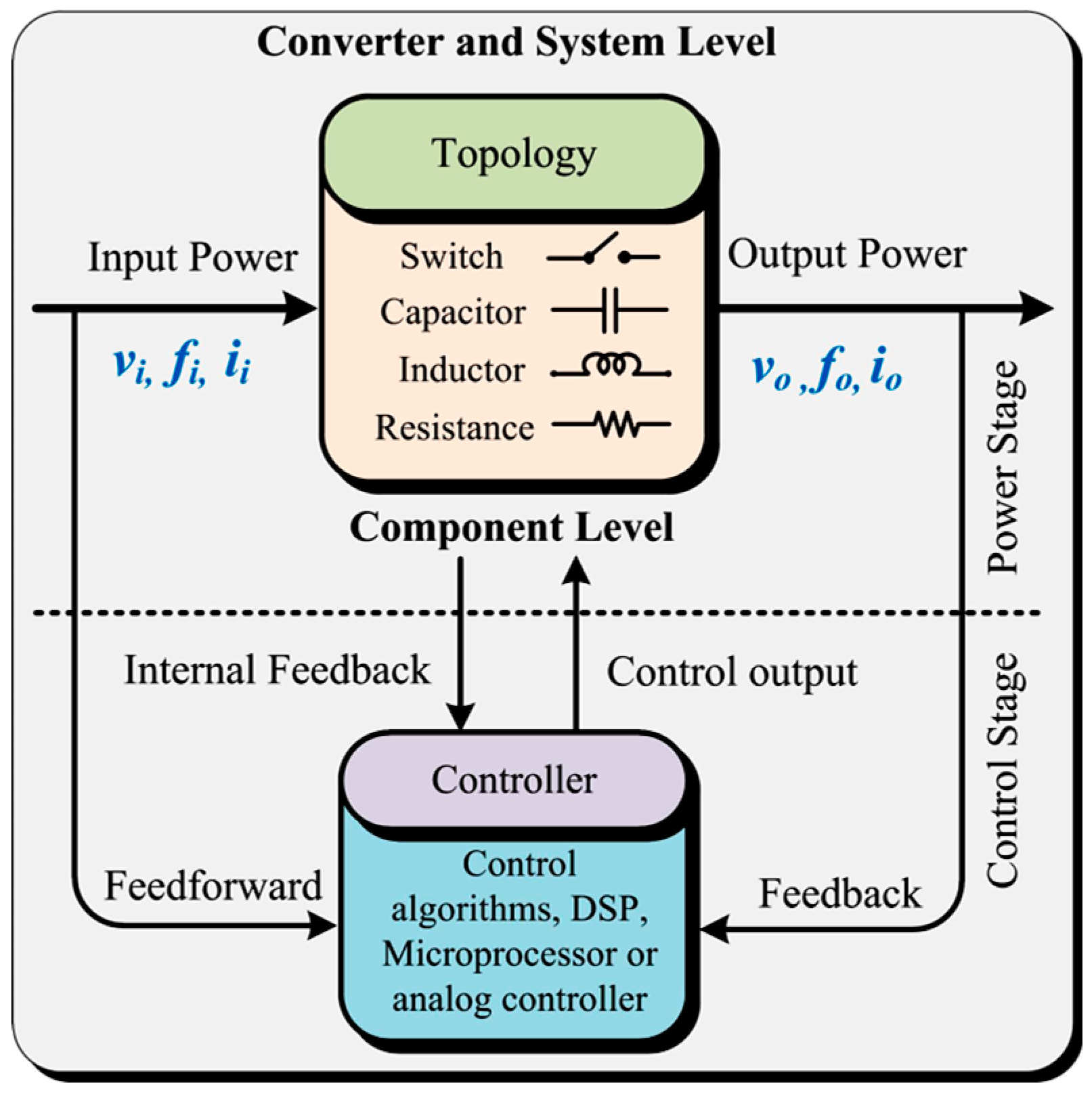
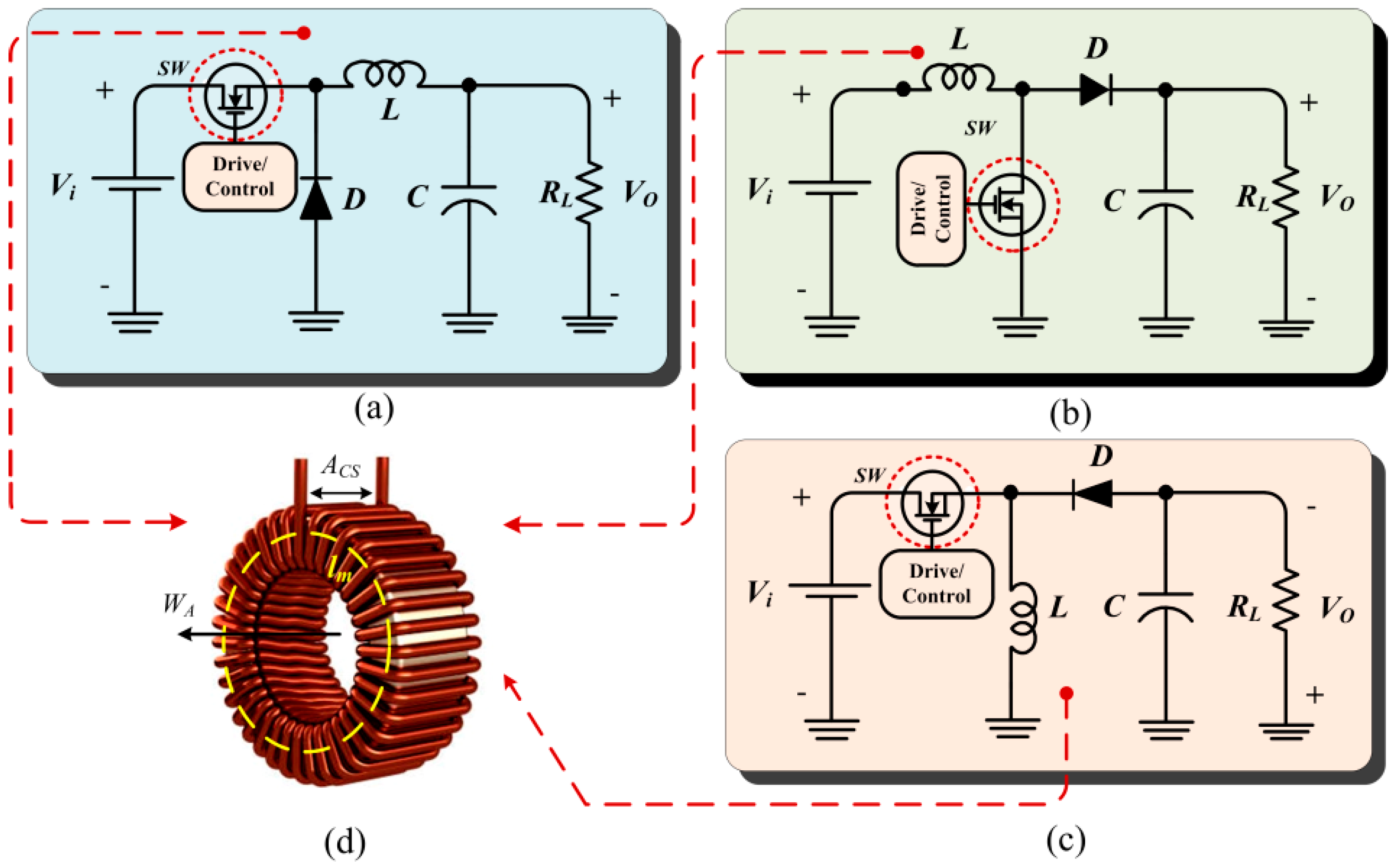
In the dynamic field of power electronics, the demand for effective and versatile energy conversion has resulted in significant advances in converter technologies. DC-DC converters, in particular, are critical for enabling voltage conversion in a wide range of applications, including portable electronic devices, renewable energy systems, and electric vehicles [1]. Figure 1 depicts the essential configuration of a power electronic converter platform, typically comprising two separate conversion stages known as the “Power” and “Control” stages [2]. In the “Power stage”, the converter receives the input electrical signal, which may be in the form of alternating current (AC) or direct current (DC) depending on the application [3,4]. Components like diodes, switches, and filters are often integrated into the input stage for conditioning and regulating the input power [5]. At the same time, the “control stages” manage the converter’s operation, encompassing controllers, sensors, and feedback loops that monitor the system’s operating conditions and adjust the converter’s behavior [6]. They include the controllers, sensors, and feedback loops that monitor the system’s operating conditions and adjust the behavior of the converter accordingly [6]. Figure 2 shows the transformerless structure of DC-DC converter topologies and illustrates the design structure of an inductor, “L” [7,8,9,10]. These structures are commonly referred to as buck, boost, and buck–boost converters. These converter topologies contain active and passive components like switches, diodes, inductors, capacitors, and resistance. In this research, the main focus has been given on the transformerless or non-isolated version of boost converter. A PID controller has been utilized to obtain the desired voltage regulation. Several researchers have reported the incorporation of PID controllers with boost converters, but settling times and overshoots still need more attention in the efficient operation of this converter at 100 and 500 kHz frequencies [11,12,13,14,15].
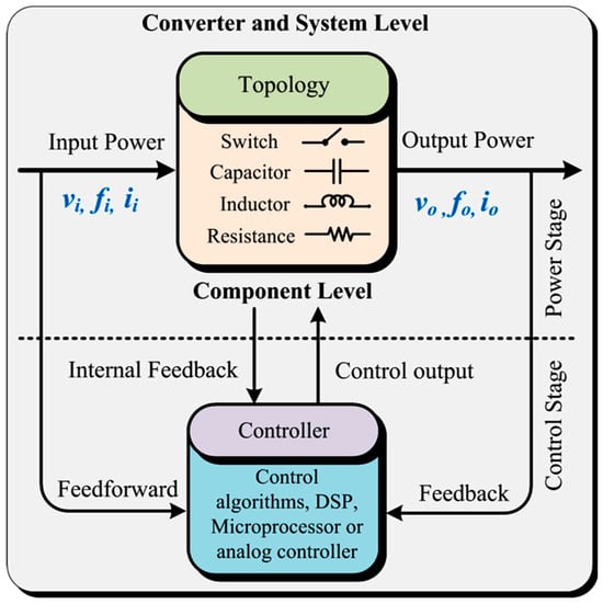
Figure 1.
The basic structure of power electronic converter.
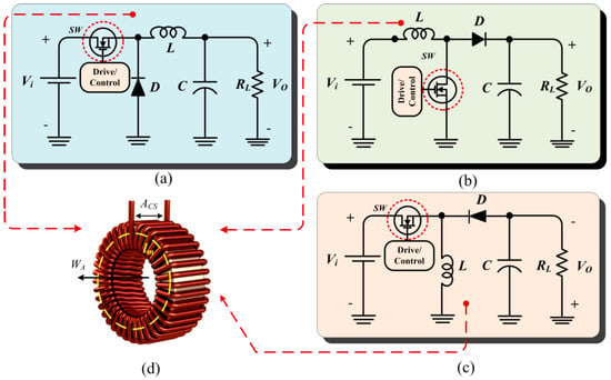
Figure 2.
Structure of transformerless DC–DC converter topologies: (a) buck converter; (b) boost converter; (c) buck–boost converter. (d) Design configuration of inductor, “L” (toroidal).
Essentially, the inductor, “L”, retains the energy in the form of a magnetic field. Due to this property, it is also known as a Magnetic Energy Storage Element (MESE) [16]. It typically consists of a coiled wire wound around a core material that is made up of ferromagnetic material [17,18,19]. Within various converter configurations, the inductor, “L”, plays a crucial role in enabling the energy transfer and conversion process, ensuring constant output voltage levels while controlling the switching operations. Various reports have been made related to the derivation of inductance value instead of proper design criteria and evaluation process, which still need proper attention [17,18,19,20].
In the field of electronics and power engineering, reliability and failure rates are the fundamental elements that ensure the expected performance of components, devices, and systems [21,22,23]. Assessing reliability through an analysis of failure rates is a crucial process, providing insights into the operational dependability and lifespan of components in DC-DC converters. Determining the rate of failure for each component yields an important understanding of the performance characteristics of individual components in terms of failure behavior, serving as valuable information for product design engineers [24,25,26]. The following research work was incorporated into this research paper:
- ❖
- A comprehensive performance analysis has been carried out for a 48-watt ( = 12 V, = 24 V, = 2 A, and = 100 kHz) transformerless DC-DC boost converter. The converter was designed and simulated with the help of a PID controller used for achieving precise regulation of the output voltage and ensuring a rapid response to disturbances through dynamic modeling. The PID controller is a feedback control system that adjusts the control input based on the error (the difference between the desired set-point and the measured process variable).
- ❖
- Further, to check the behavior of linear time-invariant systems and system stability, frequency response analyses were carried out using Bode plots at 100 kHz and 500 kHz frequencies.
- ❖
- Performance comparisons were made for uncompensated and compensated transformerless boost converters at 100 kHz and 500 kHz switching frequencies.
- ❖
- In this research paper, the converter’s performance analysis was carried out with special attention to inductor design and component reliability evaluation.
- ❖
- For the design of the inductor “L”, the “Area Product Technique (APT)” has been used to analyze the factors likewise window area (), magnetic length (), cross-section area (), number of turns (N), and size of wire (in SWG) [16,17,18,19,20,21,22].
- ❖
- Further, a performance investigation of the inductor “L” was carried out as a function of load current, supply voltage, and load resistance at 100 and 500 kHz frequencies.
- ❖
- Furthermore, considerable attention was directed towards analyzing the reliability and failure rates of active and passive components within a 48-watt transformerless DC-DC boost converter. These analyses offer valuable insights into the anticipated operational longevity and potential failure patterns of each component within a 48-Watt transformerless DC-DC boost converter. The evaluation of reliability contributes significantly to comprehending the component’s enduring performance.
2. The Modeling of a Transformerless DC-DC Boost Converter
The modeling of converters is necessary because it offers a deep understanding of their operation, facilitates design and optimization, supports control system development, ensures stability, and predicts performance. In a boost converter, by adjusting the on-time and off-time of the switch (duty ratio), the output voltage can be regulated to the desired level. The duty ratio “K” is expressed as Equation (1):
The ripple current, , was evaluated by Equation (2):
Similarly, the value of the inductor “L” was evaluated using Equation (3):
And further, the value of capacitor “C” was evaluated using Equation (4):
Likewise, the total power losses “” and efficiency were calculated by utilizing Equations (5) and (6) accordingly:
and
For the transformerless DC-DC boost converter’s modeling process, two dynamic switching situations have been considered: first, when the switch is “ON”, and another case when the switch is “OFF”, as depicted in Figure 3a. The fundamental state space equation model has been shown in Equation (7).
where , , , and = system matrices, = state variable, = state variable derivatives, = input, and = output.

Figure 3.
Dynamic switching states for modeling of transformerless DC–DC boost converter. (a) State I: switch turned “ON”. (b) State II: switch turned “OFF”.
In each circuit state, the linear circuit is characterized using a state-variable vector denoted as “”, which includes the inductor current and the capacitor voltage. Lowercase letters are employed to represent variables, encompassing their steady-state DC values along with small AC perturbations, such as .
During , when the switch is “ON” for mode 1, the state and output equations can be considered as Equation (8):
Equation (8) is also known as the “Large signal model” during the period “KT”. The state equations for the above mode can be written by applying Kirchhoff’s law in both loops (refer to Equation (9)):
Here, the output voltage “Vo” is constant; anything divided by “RL” can effectively be replaced by a constant current source as “”.
Further, during the time interval the switch is “OFF”, as shown in Figure 3b. During , the state and output equations can be considered as (refer to Equation (10)):
Equation (10) is also known as the “Large signal model” during the period ‘’. The state equations for the above mode can be written by applying Kirchhoff’s law in both loops (refer to Figure 3b) and ultimately can be written as (refer to Equation (11)):
Further, the fundamental state space-averaged model is shown (refer to Equation (12)):
To produce an average description of the circuit over a switching period, combining both “large signal models” using the state space averaging method for modes 1 and 2, given by Equations (9) and (11), ultimately provides an “Average large signal model” and can be written in the form of Equation (13).
After combining, the average large signal model can be represented in the form of Equation (13). So, before combining, we consider K = k. So, combining both modes for KT and (1 − K)T using averaging methods, we obtain:
So, after solving Equation (14), we obtain (refer to Equation (15))
Here, Equation (15) is known as the “Average large signal model”. So, now from the “Average Large Signal Model”, the “Steady-State Model” shall be obtained. For this, all derivative terms become zero and all variables change into upper case. So, by putting = 0, k = K, = , = , and = into Equation (16), we obtain:
Equation (16) is known as the “Steady-State Model”. In Equation (15), the matrix “” is time-varying due to the presence of “k”, so we have to convert it into a “Time invariant matrix”. This linearization technique is used when the steady-state part is removed and another input “” is added.
Small ac perturbations, represented by “^”, are introduced in dc steady-state quantities, or we can say that “Large signal model” is reduced to a “Small-signal model”. Therefore, for this first scenario, we must map the state variables as where “K” is the steady-state part and is the small-signal part. So, from Equation (15), we obtain:
Further, solving Equation (17), we obtain
Equation (18) is known as the “Small-Signal Model”. From this model, the control voltage gain, transfer function for load disturbance, and voltage transfer function can be obtained.
3. The Employed Control Technique
The closed-loop control scheme is depicted in Figure 4 for the transformerless DC-DC boost converter. These converters step up the input voltage to provide a stable output voltage. However, they are subject to fluctuations in the input voltage and load conditions, which makes it imperative to implement sophisticated control techniques for optimal performance. A PID controller [11,14] is a versatile and widely adopted control strategy known for its ability to maintain precise output voltage regulation.
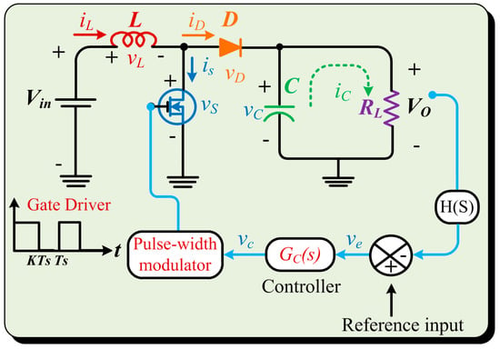
Figure 4.
The closed–loop control scheme of transformerless DC–DC boost converter.
Proportional–Integral–Derivative (PID) Controller
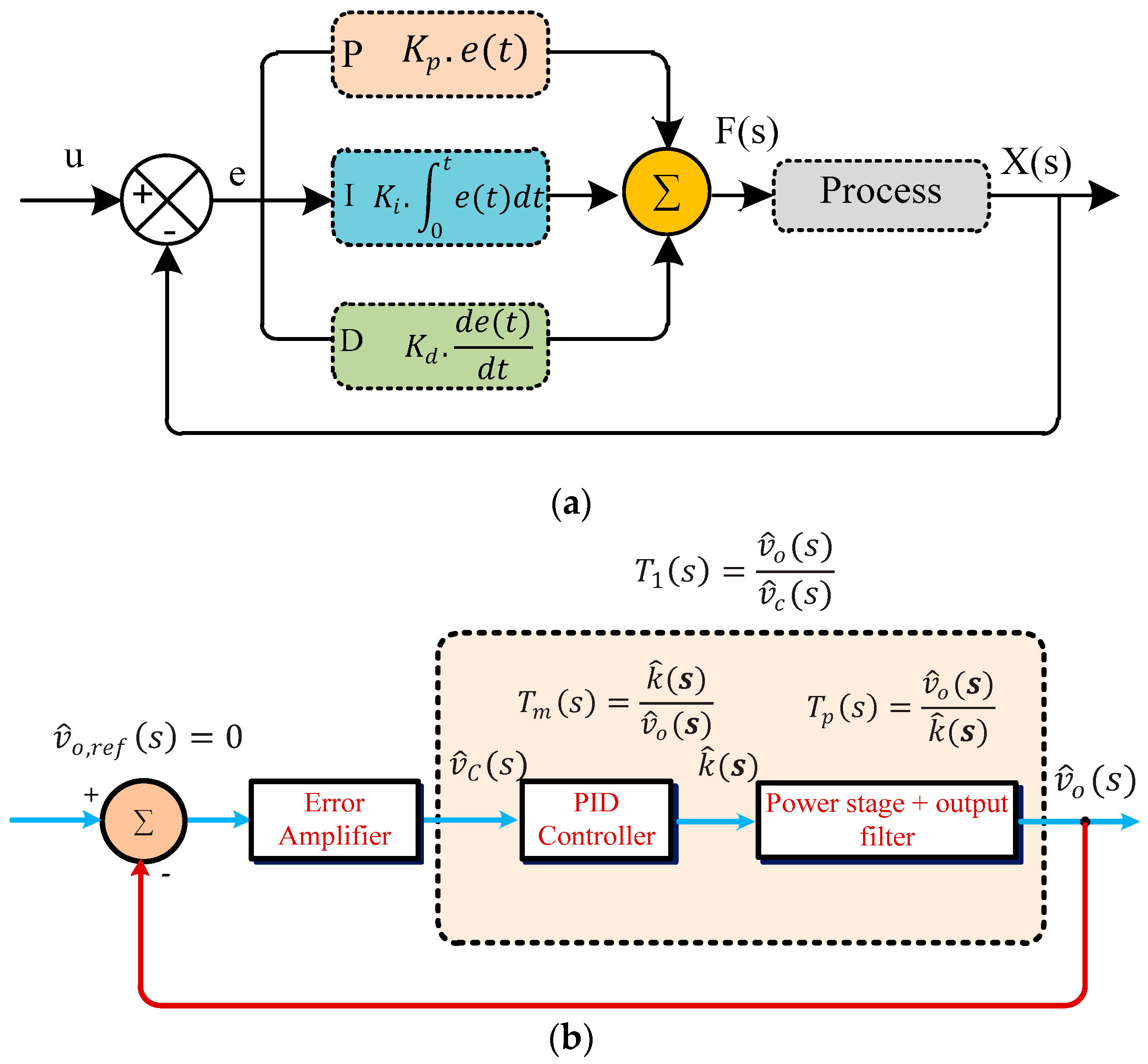
A PID controller (refer to Figure 5a) is a feedback control loop mechanism that continually calculates an error signal as the difference between a desired set-point (reference) and a measured process variable (output).
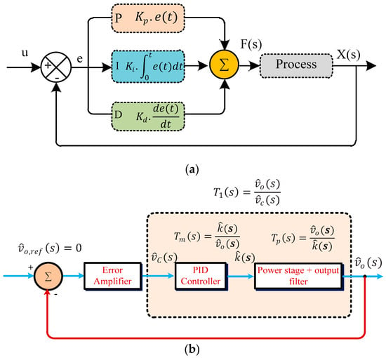
Figure 5.
Control scheme. (a) Proportional–Integral–Derivative (PID) controller; (b) linearized feedback control system for transformerless DC–DC boost converter.
The controller applies the proportional, integral, and derivative terms to the error signal to compute the control output, which adjusts the system’s process to bring the output closer to the desired set-point [15,16,17,18,19,20,21,22,23,24,25,26,27].
- Proportional (P) term: The P-term generates a control output that is directly proportional to the current error, thereby determining an immediate corrective action based on the error’s magnitude. In boost converters, the P-term helps reduce steady-state errors by adjusting the duty cycle of the switches.
- Integral (I) term: The I-term integrates the error over time and applies corrective actions to eliminate prolonged steady-state errors. In boost converters, the I-term aids in removing offset voltage and ensuring tight regulation.
- Derivative (D) term: The D-term anticipates future errors by analyzing the rate of change of the error signal. It provides a control action to mitigate rapid changes, improving the converter’s transient response and stability.
An illustration of the PID control technique is presented in Figure 5a [28,29]. In this diagram, the input signal is denoted as u(t), and the controller’s output is expressed as “F(t)” (refer to Equation (19)):
Middlebrook, along with Cuk and their colleagues from the California Institute of Technology, introduced a steady-state averaging technique. This method yields a linear model of the power stage, which includes the output filter as shown in Figure 5b, but it is specifically designed for small signals. This linearization process is performed around a stable, DC-operating point. Further, the effect of the above parameters on the stability of the closed-loop system is listed in Table 1.

Table 1.
Effect of tuning parameters of PID controller (“ ”: increasing, “
 ”: decreasing).
 ”: increasing, “
 ”: decreasing).
4. The Design of an Inductor in a 48-Watt Transformerless DC-DC Boost Converter
The inductor “L” plays a significant role in achieving voltage boosting and efficient power conversion in various electronic applications, such as renewable energy systems, mobile devices, electric vehicles, battery charging, and LED drivers [20]. Inductors, “L”, store energy in their magnetic fields during the on-time of the switching cycle and release it during the off-time, effectively raising the output voltage. Further, this stored energy is transferred to the output during the off-time of the switching cycle. This energy transfer allows for a voltage step-up without the need for a bulky and costly transformer, making transformerless boost converters more compact and cost-effective [20,22]. The optimal design of the inductor is a significant challenge and also an essential requirement to ensure the optimal performance of the converter in various applications.
4.1. Factors Related to the Inductor Design
In the process of designing inductors, various factors like the selection of core materials, considerations surrounding the saturation of magnetic cores, and the suitability of magnetic core types emerge as important determinants in achieving optimal outcomes [16].
In addition to core material selection, it is also important to understand the physics of saturation in magnetic cores, analysis of inductor power loss and self-heating with allowable ripple currents, etc. [30,31,32].
4.1.1. Magnetic Core Saturation: Reasons and Impact
Saturation in the context of inductors refers to a case where the magnetic flux in the core attains its highest limit. When the magnetic field in the core increases beyond a certain point, the core material becomes saturated, and further increases in current do not result in a proportional increase in magnetic flux [32,33].
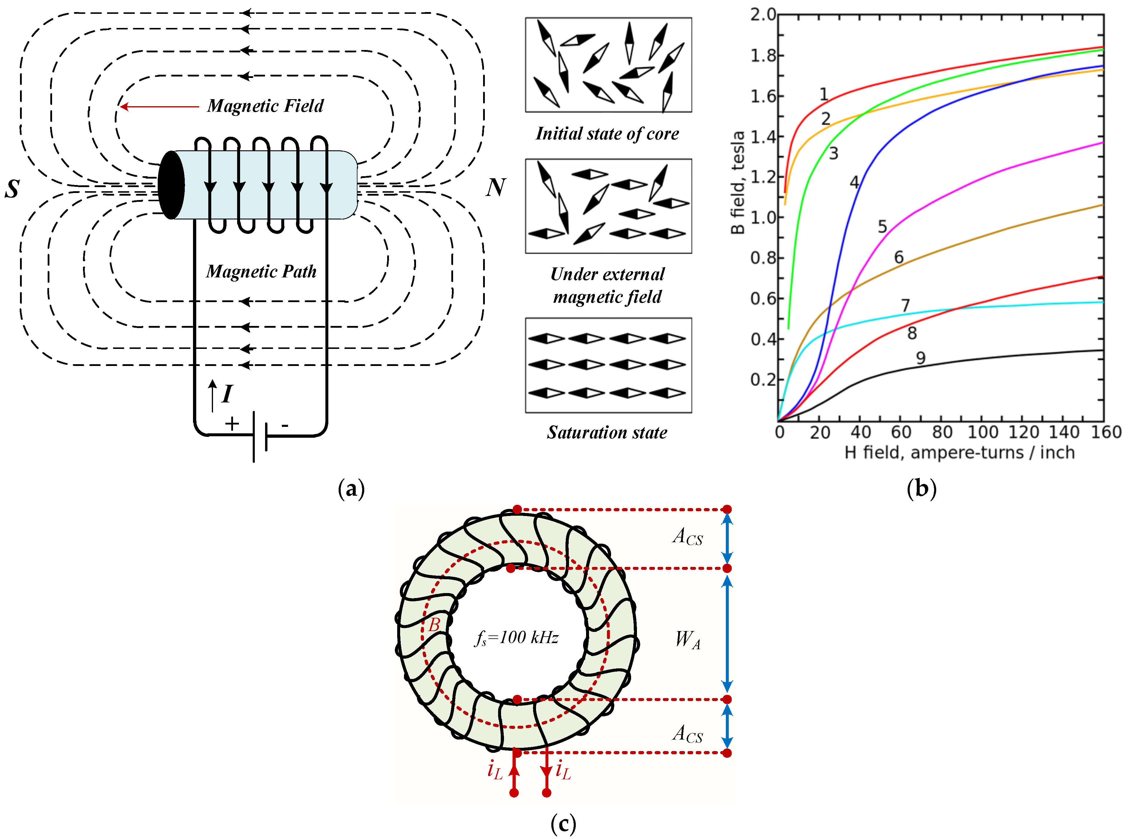
When an electric current flows through the coil as shown in Figure 6a, it generates a magnetic field. The magnetic core is then magnetized through this magnetic field, causing its internal magnetic domains to undergo a slow rotation. Once the magnetic core is fully magnetized, the orientation of the magnetic domains aligns continuously with the magnetic field, as shown in Figure 6a. At this point, even if an external magnetic field is provided, the core no longer has rotating magnetic domains, indicating that the inductor has reached a state of saturation.

Figure 6.
Perspectives of inductor saturation and its structure: (a) inductor with DC excitation with core saturation process; (b) BH curve for different materials (1: sheet steel, 2: silicon steel, 3: cast steel, 4: tungsten steel, 5: magnetic steel, 6: cast iron, 7: nickel, 8: cobalt, 9: magnetite); (c) the schematic of inductor “L” structure (toroidal).
Saturation is observed in the BH curve of a material, characterized by a rightward bend in the curve as shown in Figure 6b. As the “H” increases, the “B” approaches a maximum value asymptotically, representing the saturation level for the material. Beyond saturation, the “B” field continues to increase but at a much smaller paramagnetic rate compared to the ferromagnetic rate observed below saturation, as illustrated in Figure 6b [33].
The relationship between the magnetizing field “H” and the magnetic field “B” can be expressed as the magnetic permeability “”. It is important to note that the permeability of ferromagnetic materials is not constant but varies with “H”. In saturated materials, the relative permeability increases with “H” until it reaches a maximum. Subsequently, as it approaches saturation, the relative permeability reverses and decreases towards one [34].
4.1.2. The Selection of Core Material
Selecting the appropriate core material is important in inductor design for optimal performance and efficiency. The material’s magnetic permeability affects the inductance, while saturation levels prevent distortion at high currents. Minimizing hysteresis and eddy current losses is crucial for efficiency. Core materials have distinct frequency responses, and temperature stability ensures reliable performance. Balancing these factors with cost considerations is essential for a successful and cost-effective inductor design [31].
4.1.3. Losses and Self-Heating
During the design of an inductor, it is important to focus on the losses and the subsequent self-heating of the components. Losses in inductors primarily arise due to core losses and copper losses:
(i) Core losses: Core losses have hysteresis and eddy current loss. Hysteresis losses occur due to cyclic magnetization and demagnetization of the inductor’s core material. As the magnetic field reverses, the core is influenced by a hysteresis loop, leading to energy dissipation in the form of heat. Similarly, due to variations in the magnetic field, eddy currents are introduced in the core material. These circulating currents result in resistive heating, contributing to overall core losses [35].
(ii) Copper losses: These losses occur in windings due to the resistance of the wire. When a current flows through the coil, heat is generated in proportion to the square of the current and the resistance of the wire.
The cumulative effect of these losses results in the self-heating of the inductor. The temperature rise within the inductor is influenced by factors such as the magnitude of the current, the frequency, and the thermal properties of the core materials [30]. Efficient inductor design involves minimizing these losses to prevent excessive self-heating. This can be achieved by selecting core material with low hysteresis and eddy current losses and using low-resistance conductors for winding.
4.1.4. Ripple Currents in Inductors “L”
Ripple currents in inductors refer to the AC component superimposed on the DC, flowing through the inductor in the circuits, particularly in power converters. These fluctuating currents rise due to the switching nature of converters and the charging and discharging of capacitors. These ripple currents can cause saturation, EMI issues, voltage spikes, and voltage stress in the system. So, it is important to pay careful attention to the selection of inductor parameters and their associated factors.
In this paper, the “Area Product Technique (APT)” was employed for the design and development of an inductor, “L”. It provides a systematic approach to ascertain the required core size and turn count for an inductor, ensuring adherence to specific performance criteria, including inductance and current ratings [16]. Essentially, an inductor “L” is made up of a coil and a magnetizing core. The magnetic core includes the magnetic and physical properties of the material. These properties include things like magnetic flux density or (i.e., how strongly it can attract magnetic fields), the size of its core cross-section “”, the window area “” (i.e., the space it occupies within the window), the magnetic length “” (i.e., how far its magnetic effect extends), the permeability “µ” (i.e., how it responds to magnetic fields), and various other characteristics. In the process of designing the inductors “L” , the intricate interplay between these electrical and magnetic parameters plays a crucial role, offering insights into the core material, coil wire thickness, number of windings (N), and potential consideration of an air gap length.
Figure 6c shows the toroidal shape of the inductor. The “Area Product Technique (APT)” is a structured technique that aids in the design of inductors for switching power supplies.
4.2. Evaluation of the Window Area ()
For calculating the window area ‘’, the mathematical relationship between N and J is important to describe and is expressed as Equation (20):
where ‘’ is the “window utilization factor” and “J” is the current density .
The maximum value “” and the root mean square value “” of the inductor current are expressed by the crest factor “” (refer to Equation (21)) that replicates the current wave shape through the inductor.
From Equations (20) and (21), the can be obtained as (refer to Equation (22)):
4.3. Evaluation of the Area Product ()
As per Faraday’s electromagnetic induction law,
After integrating Equation (23), it is given as:
Here, : the maximum core flux density, and : the maximum current in the inductor windings.
Whenever the current flows in an inductor “L”, energy is stored and is expressed as (refer to Equation (25)):
So, from Equations (20) and (21), the area product is given as (refer to Equation (26)):
Here, ‘’ is known as the current density expressed in .
4.4. Assessment of Permeance ()
Permeance stands as a vital parameter delineating the ease with which magnetic flux can establish itself within a material or a magnetic circuit. Its calculation is expressed as (refer to Equation (27)):
In Equation (27), and represent the permeability of free space and the relative permeability of the core material, respectively. Further, signifies the air gap length (m), indicates the length of the magnetic path of the core (in m), and represents the core cross-sectional area (.
4.5. Assessment of the Number of Turns (N) and Wire Size (a)
From the ratio of inductance and permeance, one can assess the required number of turns. Similarly, for assessing the wire size, the RMS value of the current and its density plays an important role. The number of turns “N” and wire size “a” were evaluated by Equation (28).
5. Reliability and Its Associated Factors
Reliability is a measure of the ability of a system, component, or process to perform its intended function consistently and predictably under specified conditions for a defined period. Reliability assessment involves evaluating the probability of failure, failure rate, and other metrics to ensure that a system or component meets its intended purpose. In the context of the design of an inductor “L”, reliability provides information about failure rates and chances of failure, which play an important role for designers.
Reliability is commonly represented by a distinctive mathematical function known as the “Reliability function”, expressed as “” [24]. This function quantifies the probability of a system to operate without any failures within a specified time [0, t]. “” is a mathematical expression that symbolizes the system’s capacity to sustain its operational integrity over time [25].
5.1. Failure Rate
Failure rate is often denoted as an important reliability metric used in various fields, including engineering, electronics, and quality management. It measures the possibility of a component or system experiencing a failure within a specific unit of time. The failure rate is expressed in various units, such as failures per hour, failures per million hours, or failures per operating cycle, depending on the context. It can be represented in two ways.
5.1.1. Instantaneous Failure Rate ()
The instantaneous failure rate, generally denoted as “” (lambda), represents the probability of a component failing within a small time interval. It is expressed in failures per hour or failures per unit of time (e.g., failures per minute). “” describes the rate at which failures occur in a specific time. The instantaneous failure rate can vary over time, especially in systems with wear-out processes.
5.1.2. Failure Rate in Time “”
The failure rate in time is denoted as “”, which provides information about the number of failures that occur within a specific time interval. It is essentially a discrete version of the instantaneous failure rate. is typically expressed in failures per hour or failures per unit of time over a specified time interval (e.g., failures per 1000 h). It showcases the probability of a component failing within a defined period and is used to estimate the reliability of a component or system over that time frame. Unlike the continuous nature of λ, provides information about the failure rate within discrete intervals.
Mathematically, “” is frequently expressed as the derivative of the reliability function “”, as shown in Equation (29).
The reliability function, “”, represents the probability of the remaining operation not experiencing a failure up to a specified time , and it is expressed as Equation (30).
5.2. MTTF
The Mean Time to Failure (MTTF) represents the average time between the initial operation of a component or system and the occurrence of its first failure. It is a measure of reliability and is expressed in units of time, like hours, days, or years.
Mathematically, MTTF is defined as the integral of the system’s lifetime for the time-dependent reliability function “” (refer to Equation (31)):
In cases where the failure rate is constant or nearly constant over time, the MTTF can be approximated as the reciprocal of the failure rate (refer to Equation (32)):
6. Evaluation of the Part Failure Rate of Active and Passive Elements in a 48-Watt Transformerless Boost Converter
6.1. Part Failure Rate of Inductor “L”
Reliability assessment models have failure rates and stress factors [26]. The part failure rate for an inductor “L” is given (in as (refer to Equation (33)):
The is known as the part failure rate for an inductor “L”, and application factor , quality factor , and environmental factor are known as stress factors [23,26].
6.1.1. Base Failure Rate
In the field of reliability engineering, the base failure rate, commonly denoted as , is considered a fundamental metric. It depicts the intrinsic initial probability of failure for a component or system during a specified unit of time under the prescribed operating conditions.
Mathematically, it can be described as the failure rate occurring under conditions where the different factors such as voltage, temperature, and other environments remain at their nominal values, as illustrated in Equation (34).
Here, “F(t)” depicts the total distribution failure time function.
6.1.2. Temperature Factor
It is a critical environmental variable that influences the reliability of electronic components and equipment. In the evaluation of reliability, the temperature factor [26] is denoted as and it plays a significant role in assessing the effect of temperature variations on failure rates and system performance. This factor varies from component to component. For an inductor “L”, it is expressed as (refer to Equation (35)):
where is the hot-spot temperature in ( is the ambient temperature in (, and is a change in temperature with respect to (.
6.1.3. Quality Factor
In reliability, the quality factor, also known as , is a performance factor that includes component quality and performance. Unlike its electrical and mechanical counterparts, the quality factor focuses on determining how well a component or system meets the desired reliability standards and user expectations.
6.1.4. Environmental Factor
In terms of component reliability, the environmental factor plays a vital role. It denotes the external conditions and influences present in an operational environment that can substantially affect the performance and lifespan of a component or system. Temperature, humidity, vibration, shock, chemical exposure, radiation, dust, electromagnetic interference (EMI), altitude, and more are examples of several sub-factors of the environmental factor within component reliability. Each of these sub-factors can introduce risks to a component’s reliability.
6.2. Part Failure Rate of the Switch (MOSFET)
The part failure rate of the switch (MOSFET) (in [21] is calculated as Equation (36). Here, = temperature factor, = junction temperature (in °C), = junction-to-case thermal resistance in (°C/W), = environmental factor, = quality factor, and = application factor.
6.3. Part Failure Rate of the Diode
The part failure rate of the diode [26] is calculated (in as (refer to Equation (37)):
where = junction-to-ambient thermal resistance, = environmental factor, = quality factor, = stress factor, = temperature factor, and = construction factor.
6.4. Part Failure Rate of the Capacitor
The part failure rate of the capacitor [26] is calculated (in as (refer to Equation (38)):
where = environmental factor, = quality factor, = application factor, = series resistance factor, = capacitance factor, = activation energy, and = voltage stress factor.
6.5. Part Failure Rate of the Resistor
The part failure rate of the resistor is calculated (in as Equation (39). Here, = environmental factor, = quality factor, and = capacitance factor, and = activation energy.
7. Results and Discussion
In this research, the main focus was on the performance analysis of a 48-Watt ( = 12 V, = 24 V, = 2 A, and = 100 kHz) transformerless DC-DC boost converter, with emphasis on the inductor design and evaluation of component reliability. Before going to the inductor design and active and passive component reliability stages, a design-oriented analysis of the boost converter was carried out using a PID controller.
7.1. Analysis of the 48-Watt Transformerless DC-DC Boost Converter Using a PID Controller
The duty ratio “K” (0.5 or 50%) was achieved by Equation (1). Prior to determining the value of inductor “L”, the ripple current of the converter was computed using Equation (2). The values of inductance and capacitance (L = 7.5 µH and C = 83.33 µF at 100 kHz, and L = 1.50 µH and C = 16.66 µF at 500 kHz) were obtained with the help of Equations (3) and (4). An STD15NF10T4 MOSFET was chosen that has = 100 V, = 23 A, = 65 mΩ, and = 30 nC parameters. Similarly, the RB238T-60NZ Schottky barrier diode was selected with = 40 A, = 60 V, and = 0.86 V.
After mathematical designing, the converter was simulated and analyzed in the MATLAB® Simulink platform. Figure 7 shows the output current and voltage response for the transformerless uncompensated DC-DC boost converter at 100 and 500 kHz frequencies. From the output current response of the converter at 100 kHz frequency, the preshoot, overshoot, undershoot, and settling time were observed as 0.86%, 71.55%, 1.93%, and 1.84 ms, respectively (refer to Figure 7a). Similarly, at 500 kHz, the preshoot, overshoot, undershoot, and setting time were observed as 0.86%, 71.55%, 1.38%, and 433.28 µs, respectively (refer to Figure 7a).

Figure 7.
MATLAB® Simulink results for uncompensated transformerless DC-DC boost converter. (a) Output current response at 100 and 500 kHz (desired Io = 2 A); (b) output voltage response at 100 and 500 kHz (desired Vo = 24 V).
From the observations, it is evident that at a 500 kHz frequency, the settling time of output current response frequency was very small in comparison to the 100 kHz switching frequency, as well as the improved undershoot. Both responses provided an output current () of 1.92 A at 100 and 500 kHz switching frequencies, which is not equal to the desired value ( = 2 A).
In the same fashion, the output voltage () response of the uncompensated transformerless DC-DC boost converter was recorded. At 100 kHz, the preshoot, overshoot, undershoot, and settling time were observed as 0.86%, 71.55%, 1.93%, and 1.84 ms, respectively, and further, at 500 kHz, these parameters were measured to be 0.86%, 71.55%, 1.38%, and 433.28 µs, respectively, as depicted in Figure 7b.
From the observations, it is evident that the settling time of the output voltage response at a 500 kHz frequency was very small in comparison to the 100 kHz switching frequency, as well as the improved undershoot. Both responses at 100 and 500 kHz switching frequencies provided an output voltage () of 23.06 V, which is not equal to the desired value ( = 24 V).
To obtain the desired system response, a PID (Proportional–Integral–Derivative) controller, a widely used control technique in power electronics known for its effectiveness in improving system performance and stability, was designed to control the output response of the system obtained from Equation (18), as shown in Figure 6.
Figure 8 shows the step responses of uncompensated and compensated transformerless DC-DC boost converter at 100 and 500 kHz frequencies. From the response (refer to Figure 8a), it is evident that the uncompensated boost converter at 100 kHz exhibited a rise time of 92.24 µs, a settling time of 7.8 ms, and an overshoot of 87.40%, as well as showing a high steady-state error, which ultimately do not match the required system specifications. As the system did not follow the required system response, a PID controller was implemented. After implementing and tuning the controller (compensated boost converter), the rise time reduced to 3.65 µs, the settling time to 31.26 µs, and the overshoot to 3.42%, which ultimately match the system requirements (refer to Figure 8a).

Figure 8.
Step response of transformerless DC–DC boost converter (a) for uncompensated and compensated boost converter at 100 kHz (b) for uncompensated and compensated boost converter at 500 kHz.
Further, the step response was obtained for an uncompensated and compensated transformerless boost converter at 500 kHz. From the response (refer to Figure 8b), it is evident that the uncompensated boost converter exhibited a rise time of 19.71 µs, a settling time of 1.6 ms, and an overshoot of 86.63%, and showed a very high steady-state error and poor transient response, ultimately not matching the system requirements. After the implementation of the PID controller, the rise time was reduced to 0.81 µs, the settling time to 1.28 µs, and the overshoot to 1.91%, which clearly shows a significant improvement in system response. Table 2 shows the details of the performance parameters of the step response with uncompensated and compensated conditions. This highlights the PID controller’s effectiveness in reducing transient response and enhancing steady-state performance at 100 kHz and 500 kHz frequencies. To identify the system stability, frequency response, etc., Bode plots were analyzed. Figure 9 shows the Bode responses of the uncompensated and compensated transformerless DC-DC boost converter at 100 and 500 kHz frequencies.

Table 2.
Performance parameters of step response during uncompensated and compensated conditions at 100 and 500 kHz frequencies.

Figure 9.
Bode response of transformerless DC–DC boost converter: (a) for uncompensated and compensated boost converters at 100 kHz; (b) for uncompensated and compensated boost converters at 500 kHz.
At 100 kHz, the uncompensated boost converter (refer to Figure 9a) exhibited the peak gain of 27.4 dB at 1.17e+04 rad/s frequency, a phase margin () of 4.25 deg, and a phase crossover frequency () of 2.02e+04 deg. With the PID controller, the results show a substantial decrease in peak gain to 0.29 dB at 6.06e+04 rad/s and phase crossover frequency to 1.60e+05 rad/s, along with a significant increase in the phase margin of 163.05 deg while maintaining a positive gain margin (). This clearly shows that the system performed well in terms of stability due to a higher phase and positive gain margin.
In the same fashion, the Bode response was analyzed at a 500 kHz frequency. From the results, the uncompensated boost converter (refer to Figure 9b) exhibited a peak gain of 26.8 dB at 5.47e+04 rad/s frequency, a phase margin () of 4.53 deg, and a phase crossover frequency () of 9.48e+04 deg. With the PID controller, the results show a substantial decrease in peak gain to 0.16 dB at 1.93e+05 rad/s and phase crossover frequency to 5.60e+05 rad/s, along with a significant increase in the phase margin of 167.35 deg while maintaining positive gain margin (). This also shows that the system performed well in terms of stability due to a higher phase and positive gain margin.
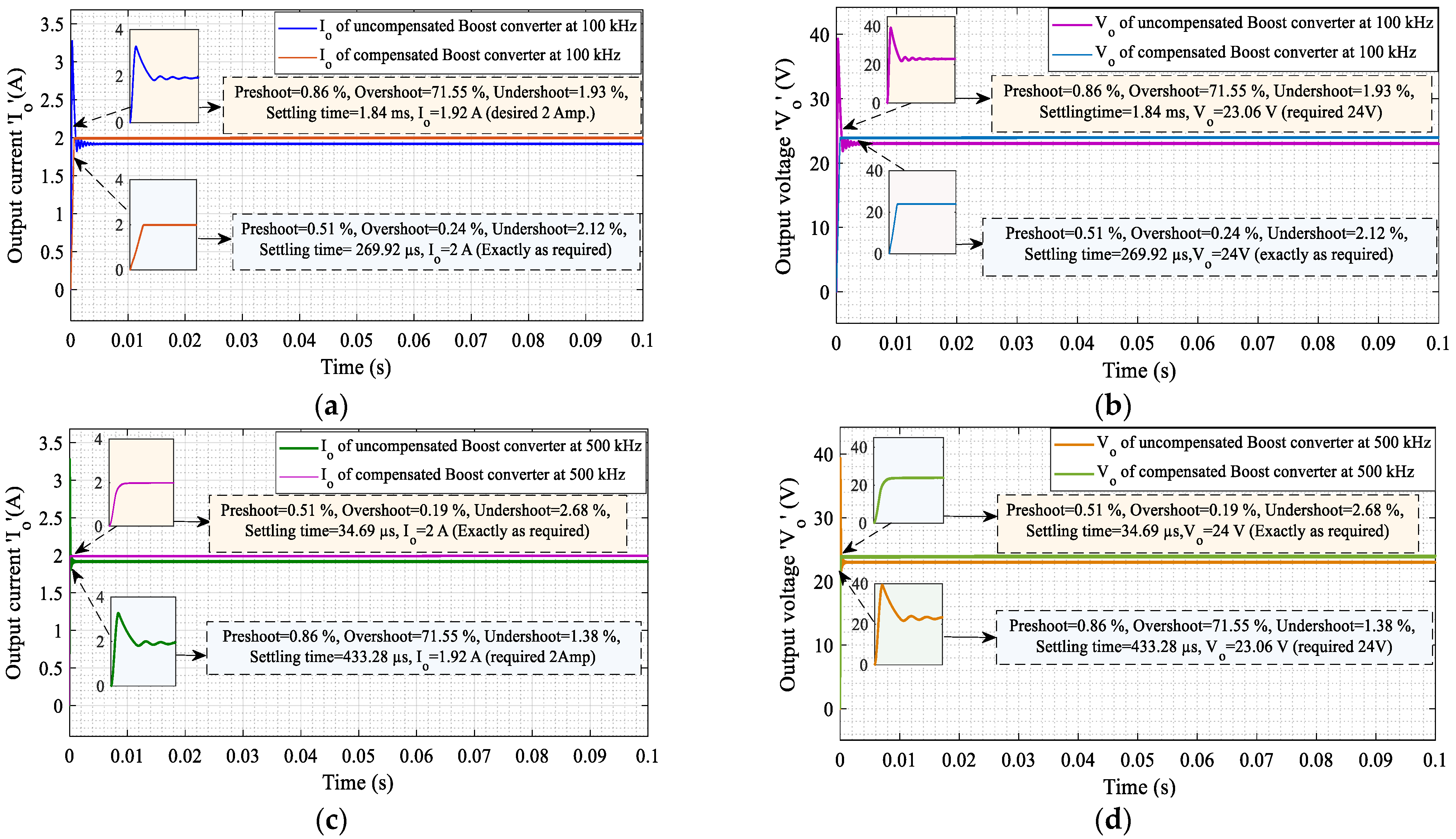
Figure 10 shows the Matlab® Simulink results of the output current () and voltage () at 100 and 500 kHz frequencies for the uncompensated and compensated transformerless DC-DC boost converters. From Figure 10a, the output current response of an uncompensated boost converter (at 100 kHz) exhibited a preshoot of 0.86%, overshoot of 71.55%, undershoot of 1.93%, and settling time of 1.84 ms, and provided a 1.92 A output current, which does not match the system requirements. Here, the system showed a high steady-state error and poor transient response. After applying the PID controller, the system showed a significant improvement in its output current response. The preshoot reduced to 0.51% and overshoot to 0.24%, the settling time improved to 269.92 µs, and it provided a 2 A output current, which meets the system requirements.
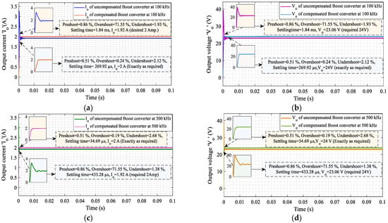
Figure 10.
MATLAB® Simulink results for uncompensated and compensated transformerless DC–DC boost converters. (a) Output current response at 100 kHz (desired Io = 2 A). (b) Output voltage response at 100 kHz (desired Vo = 24 V). (c) Output current response at 500 kHz (desired Io = 2 A). (d) Output voltage response at 500 kHz (desired Vo = 24 V).
In the same fashion, the output voltage () response for both the uncompensated and compensated boost converter is shown in Figure 10b at a 100 kHz frequency. From the results of the uncompensated boost converter, it is clear that the system exhibited a preshoot of 0.86%, overshoot of 71.55%, undershoot of 1.93%, and settling time of 1.84 ms, and provided a 23.06 V output voltage, which does not match the system requirements (24 V). Here, the system showed a high steady-state error and poor transient response. After applying the PID controller, the system showed a significant improvement in its output voltage response. The preshoot reduced to 0.51% and overshoot to 0.24%, the settling time improved to 269.92 µs, and it provided a 24 V output voltage, which meets the system requirements.
Further, the system response was recorded at a 500 kHz frequency. From the output current response as shown in Figure 10c, the uncompensated boost converter (at 500 kHz) exhibited a preshoot of 0.86%, overshoot of 71.55%, and settling time of 433.28 µs, and provides a 1.92 A output current, which does not match the system requirements. Here, again, the system showed a high steady-state error and poor transient response. After applying the PID controller, the system showed a significant improvement in its output current response at 500 kHz. The preshoot reduced to 0.51% and overshoot to 0.19%, the settling time improved to 34.69 µs, and it provided a 2 A output current, which meets the system requirements.
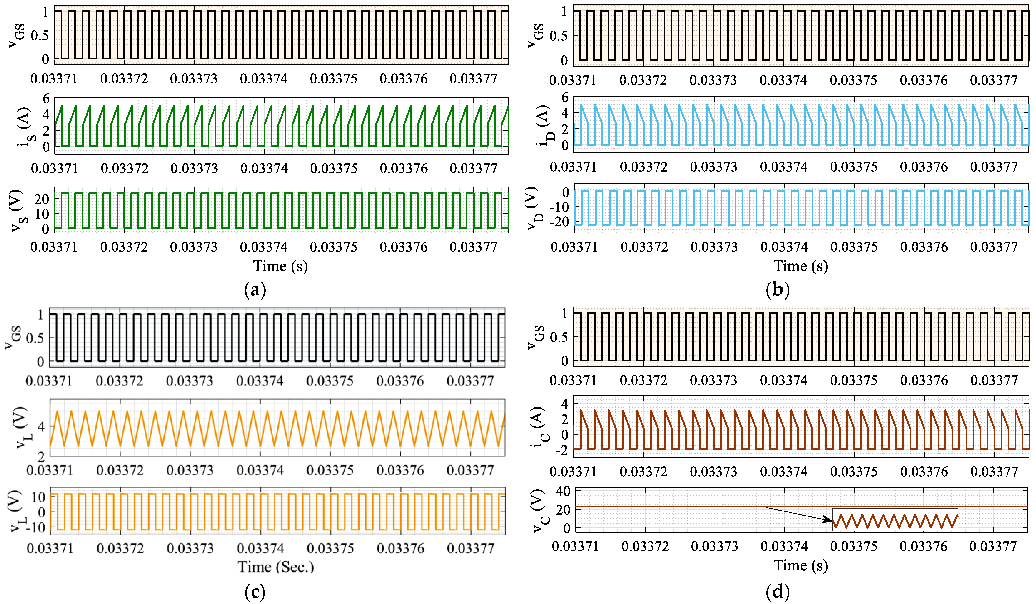
Similarly, the output voltage response of the uncompensated boost converter at 500 kHz from Figure 10d exhibits a preshoot of 0.86%, overshoot of 71.55%, and settling time of 433.28 µs, and provides a 23.06 V output voltage, which does not match the system requirements and shows the steady-state error. After applying the PID controller, the system showed a significant improvement in its output voltage response at 500 kHz. The preshoot reduced to 0.51% and overshoot to 0.19%, the settling time improved to 34.69 µs, and it provided a 24 V output voltage as required, which meets the system requirements. The findings demonstrate that the PID controller effectively reduces transient response time and overshoot, aligning the system with the desired output specifications. Furthermore, the improved stability margins achieved with the PID controller suggest enhanced performance and robustness. The performance parameters of the uncompensated and compensated boost converters are illustrated in Table 3. Figure 11 and Figure 12 show the desired Matlab® Simulation results of voltage and current across the switch, diode, inductor, and capacitor (refer to Figure 11a–d at 100 kHz and Figure 12a–d at 500 kHz).

Table 3.
Performance parameters of uncompensated and compensated 48-Watt ( = 12 V, = 24 V, = 2 A, and = 100 kHz) transformerless DC–DC boost converters.


Figure 11.
MATLAB® Simulink results: (a) voltage and current across MOSFET at 100 kHz; (b) voltage and current across the diode at 100 kHz; (c) voltage and current across inductor at 100 kHz; (d) voltage and current across the capacitor at 100 kHz.
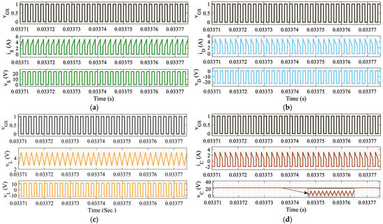
Figure 12.
MATLAB® Simulink results: (a) voltage and current across MOSFET at 500 kHz; (b) voltage and current across the diode at 500 kHz; (c) voltage and current across inductor at 500 kHz; (d) voltage and current across the capacitor at 500 kHz.
7.2. Design and Analysis of Inductor “L” in a 48-Watt Transformerless DC-DC Boost Converter
The inductor “L” was designed by utilizing the “Area Product Technique”. Equations (20), (21), and (25) were utilized to determine the fundamental elements such as the window utilization factor, the crest factor , and energy stored in the “L”. After careful evaluation, the values were obtained as = 0.6, = 4, and .
The area product was calculated using Equation (26), resulting in = 266.66 by considering a flux density wb/m2 and . Subsequently, the core with a higher area product than the calculated (266.66 ) was selected [16]. A T44-26 toroidal iron powder core [16] was chosen for the inductor “L” design. The identified core exhibits an area product ‘’ of , Similarly, at 500 kHz, a T30-26 toroidal iron powder core [16] was chosen that exhibits an area product of . The number of turns and wire size were calculated using Equation (28). From the results, 18 turns with a wire size of 19 SWG were required for the inductor at 100 kHz. Similarly, at 500 kHz, the inductor needed 10 turns with 19 SWG wire.
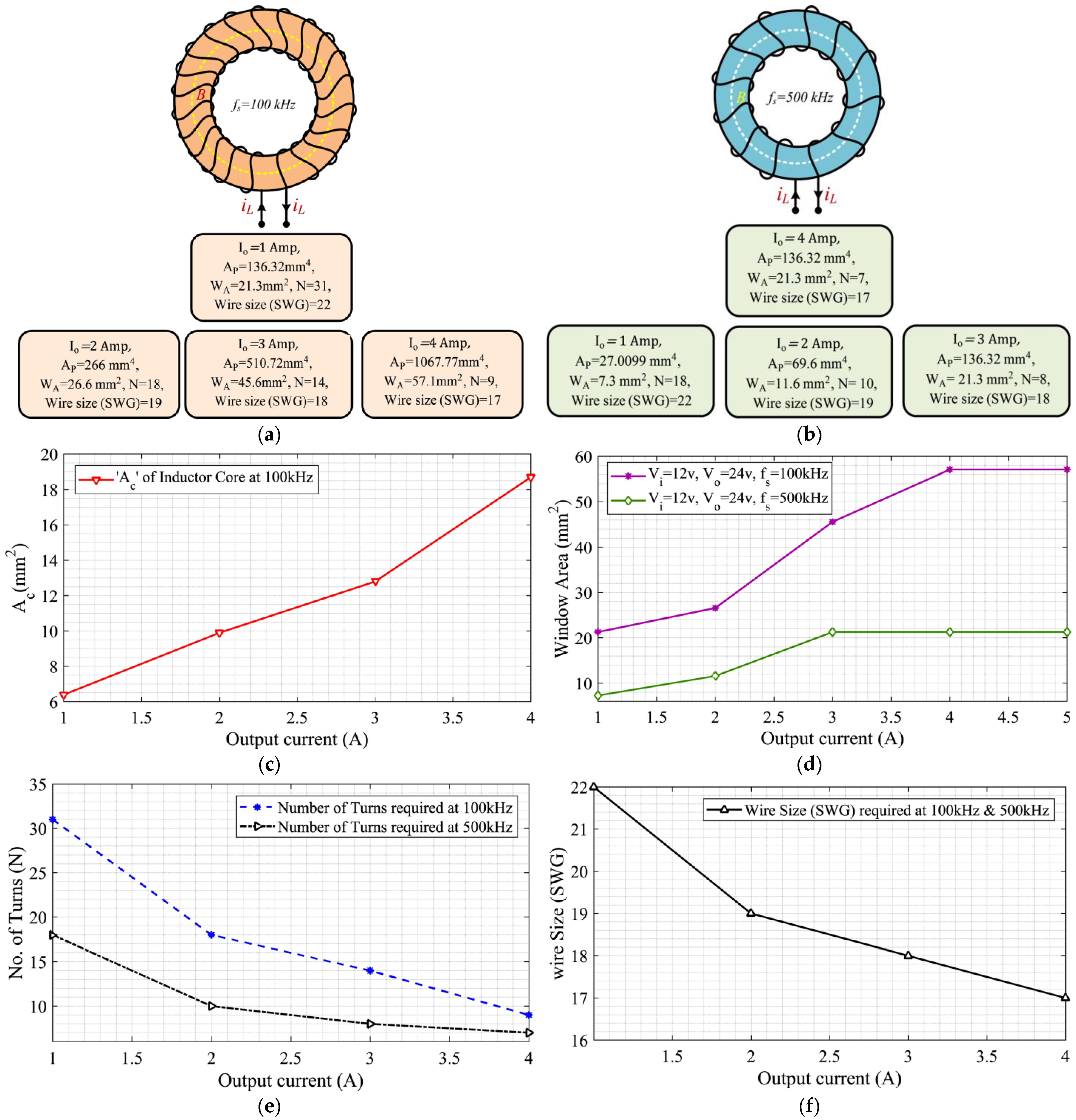
Design-oriented analysis was conducted across various output current levels (1 to 4 A), utilizing Equations (20)–(26) and, subsequently, Equations (27) and (28). The design outcomes of inductor “L” for a transformerless DC-DC boost converter are shown in Figure 13.
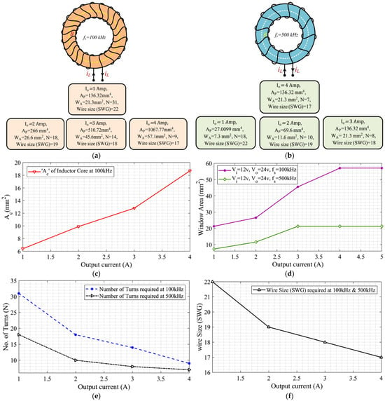
Figure 13.
Design outcomes of inductor “L” in 48-watt transformerless boost converter for Vi = 12 V: (a) design of inductor at a frequency of 100 kHz; (b) design of inductor at a frequency of 500 kHz; (c) core cross-sectional area “Acs” vs. output current at 100 kHz; (d) window area vs. output current at 100 and 500 kHz; (e) number of turns “N” vs. output current at 100 and 500 kHz; (f) wire size (SWG) vs. output current at 100 and 500 kHz.
The findings clearly show that when the load current increases, the area product and window area ) of the inductor experience a proportional increase. Also, as the load current rises from 1 A to 4 A, the number of turns (N) decreases, and at the same time, the wire size (measured using “SWG” or Standard Wire Gauge) also gets smaller.
In Figure 13a,b, the chosen toroidal cores are presented that reveal the parameters obtained through analysis in terms of the number of turns, SWG, and area product. The performance of inductor “L” was examined at 100 and 500 kHz frequencies. The findings indicate that at higher frequencies, the size of inductor “L” decreases compared to 100 kHz, consequently reducing the core and window size (refer to Figure 13c,d). As an outcome, to design the inductor “L” for a 48-watt ( = 12 V, = 24 V, = 2 A, and = 100 kHz) transformerless DC-DC boost converter, a T44-26 iron powder core with an area product of 266 mm4 and window area of 26.6 mm2, that needs 18 turns with a wire of 19 SWG with a diameter of 1.08 mm and area of , is needed.
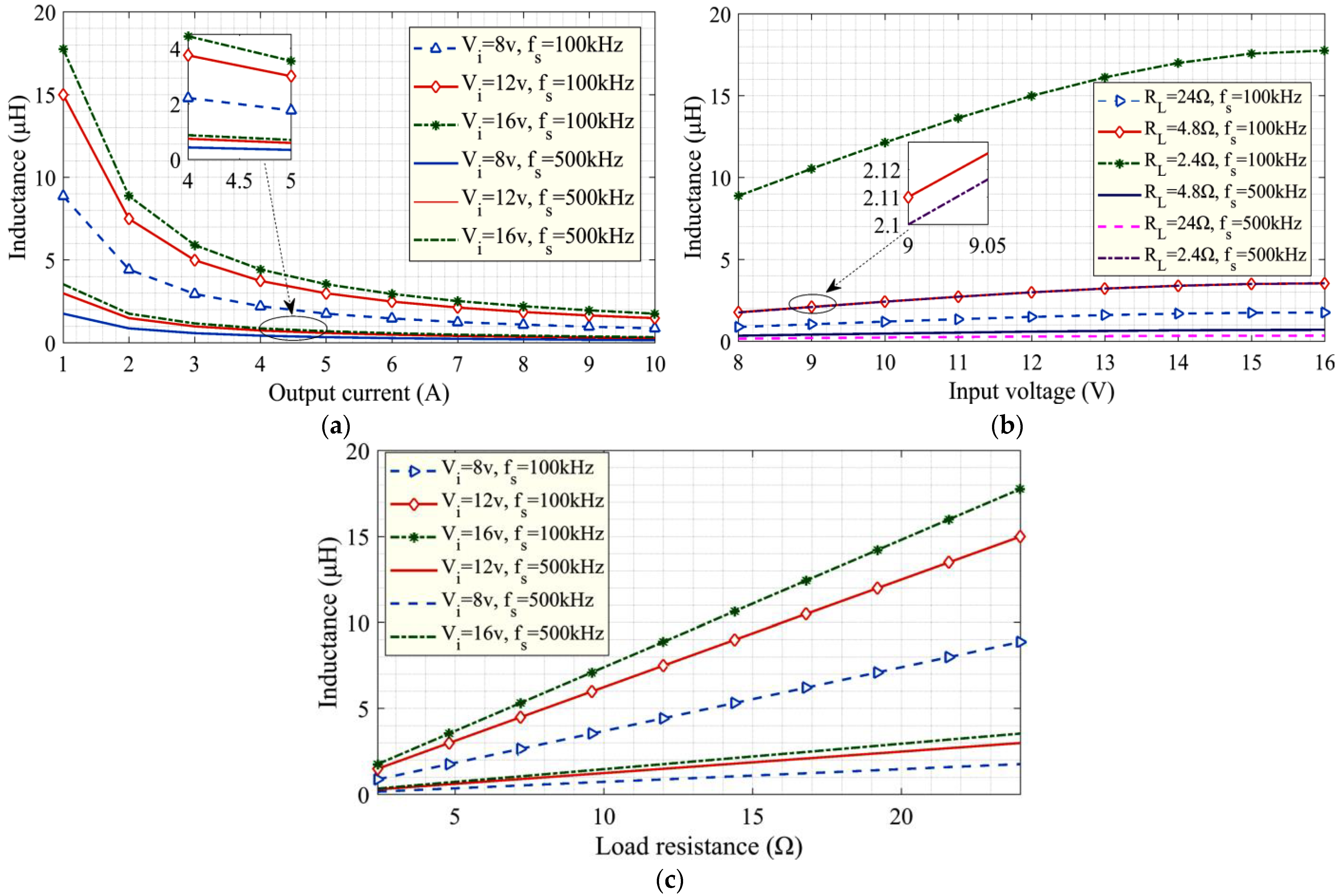
Similarly, at 500 kHz, a T30-26 toroidal iron powder core was chosen that exhibited an area product of and required 10 turns with a wire size of 19 SWG. The performance of the inductor “L” was thoroughly examined under various supply voltage and load conditions to understand its behavior at both 100 and 500 kHz. Figure 14 depicts the assessment of the inductor’s performance concerning load current (refer to Figure 14a), supply voltage (refer to Figure 14b), and load resistance (refer to Figure 14c) under different fixed input voltages and load conditions.
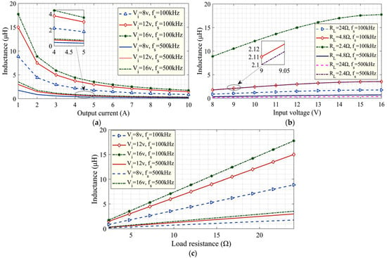
Figure 14.
Performance evaluation of inductor “L” at 100 and 500 kHz. (a) Response as a function of output current at = 8 V, 12 V, and 16 V. (b) Response as a function of input voltage at = 2.4 Ω, 4.8 Ω, and 24 Ω. (c) Response as a function of load resistance at = 8 V, 12 V, and 16 V.
At 100 kHz, it is evident that with a rise in the load current, the inductance diminished. Conversely, at fixed input voltages (8 V, 12 V, and 16 V), the inductance showed an increment. Additionally, the examination was conducted under diverse load conditions, demonstrating that variations in the load correspond to an increase in inductance.
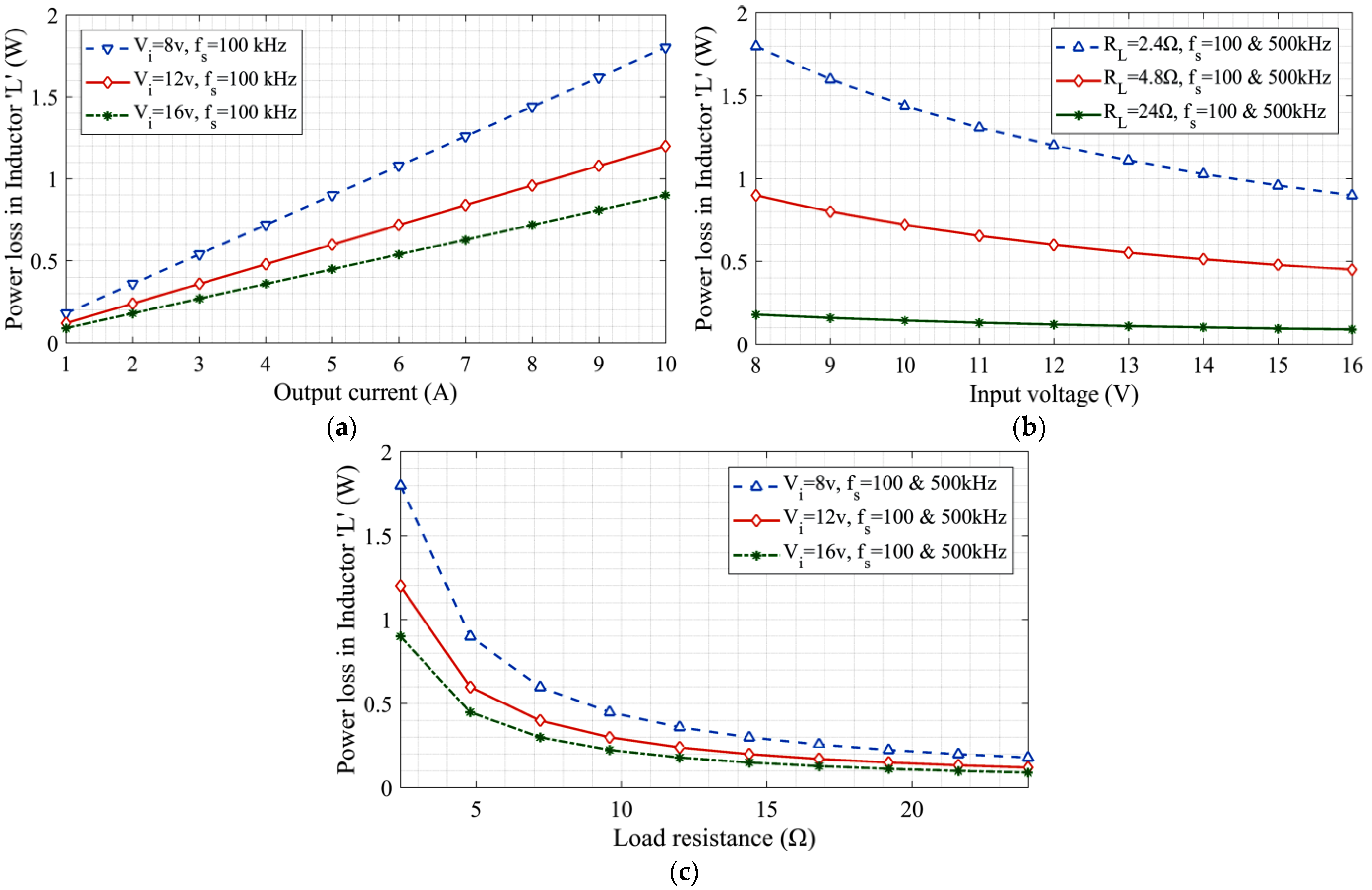
The responses were also examined at a frequency of 500 kHz, revealing that at elevated switching frequencies, the needed inductance was minimized, resulting in a subsequent reduction in core size. Further, the behavior of inductor “L” was examined by analyzing the losses at 100 and 500 kHz frequencies as a function of the output current, input voltage, and varying load conditions, as shown in Figure 15.
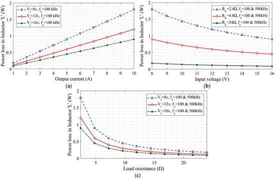
Figure 15.
Performance evaluation of inductor “L” through power loss assessment at 100 and 500 kHz frequencies. (a) Losses versus output current at = 8 V, 12 V, and 16 V. (b) Losses versus input voltage at = 2.4 Ω, 4.8 Ω, and 24 Ω. (c) Losses versus load resistance at = 8 V, 12 V, and 16 V.
The examination of power losses in inductor “L” provides significant insights. From the results, it is evident that as a function of load current, power losses in inductor “L” increased at both 100 and 500 kHz frequencies. Interestingly, it was observed that there was not so much difference in losses at the 500 kHz frequency in comparison to the 100 kHz frequency (refer to Figure 15a). It is also evident that inductors are less affected (in terms of power losses) at higher switching frequencies in comparison to other active components. Further, the losses were analyzed as a function of input voltage (refer to Figure 15b) and load resistance (refer to Figure 15c), which affect the power loss behavior of inductor “L”.
Generalized Guidelines for Inductor Design in Transformerless DC-DC Converters
In this paper, the design of an inductor for a particular 48-watt transformerless DC-DC boost converter is reported in a comprehensive manner through the “Area Product Technique (APT)”. In this particular section, efforts are made to provide a generalized guideline for inductor design, not only for boost converters but also for other transformerless DC-DC converters.
- Before going through the “Area Product Technique (APT)”, the ripple current and inductor value should be calculated according to the type of transformerless DC-DC converter topologies (using Equations (2) and (3) in the case of a boost converter).
- For designing an inductor, it is essential to obtain the mathematical information about the stored energy in the inductor .
- The crest factor ( should be evaluated according to the load current (as per the converter configuration and specifications) so that it can be used in the calculation of the area product ().
- For designing the inductor, the “window utilization factor (” can be considered as 0.6 for single-winding and 0.3 to 0.4 for multi-winding inductors.
- Further, the current density can be considered as .
- The flux density can be selected as 0.25, 1.5, and 1 for ferrite, amorphous, and CRNGO cores, respectively.
- From the datasheets [16], the core which has a higher area product than the evaluated values should be chosen in order to maintain the performance and safety margins (factors like saturation margin, temperature rise, core saturation, etc.).
- The evaluation of the number of turns and wire size can be accomplished through Equation (28). In this context, it is advisable to opt for a wire gauge with a cross-sectional area exceeding the calculated value using datasheets [16] in order to reduce the resistive losses and voltage drops, and for improving the long-term performance.
7.3. Analysis of Failure Rates and Reliability
In continuation from designing the inductor, a reliability assessment was carried out to further investigate the performance of inductor “L”, which is characterized by failure rates. For this purpose, the reliability and failure rates of each component were evaluated and compared. Here, the Military Handbook 217F was utilized for the selection of stress factors [26]. Table 4 shows the parameters used for a reliability evaluation of the components. To determine the failure rate of inductor “L” (), “” was chosen to be 0.000030. Further, ‘’ was calculated using Equation (35) as 1.9144. Similarly, ‘’ and ‘’ were selected as 3 and 6, respectively.

Table 4.
Operating parameters used during reliability evaluation of components (NA: not applicable).
Using Equation (35), the failure rate of inductor “L” was obtained as 0.0010 failure/106 h. Similarly, the failure rate of the switch (MOSFET) “” was calculated using Equation (36). The “” was chosen to be 0.012. Here, the ‘’ was calculated by selecting the hot-spot temperature using the MOSFET datasheet as 1.5335. Further, the ‘’, ‘’, and ‘’ were selected as 5.5, 8, and 6, respectively.
After calculating all the factors, the failure rate of the switch (MOSFET) was calculated as 4.8580 failure/106 h using Equation (36).
Similarly, in the case of the diode, the failure rate “” was calculated as 0.0230 failure/106 h using Equation (37). Here, the ‘’ was calculated as 2.1510 using Equation (37). Further, the , ‘’, ‘’, and ‘’ were calculated as 0.1078, 5.5, 6, and 1, respectively. Similarly, the failure rate was calculated for the capacitor “” and load “” using Equations (38) and (39) as 0.0717 failure/106 h and 1.7265 failure/106 h, respectively.
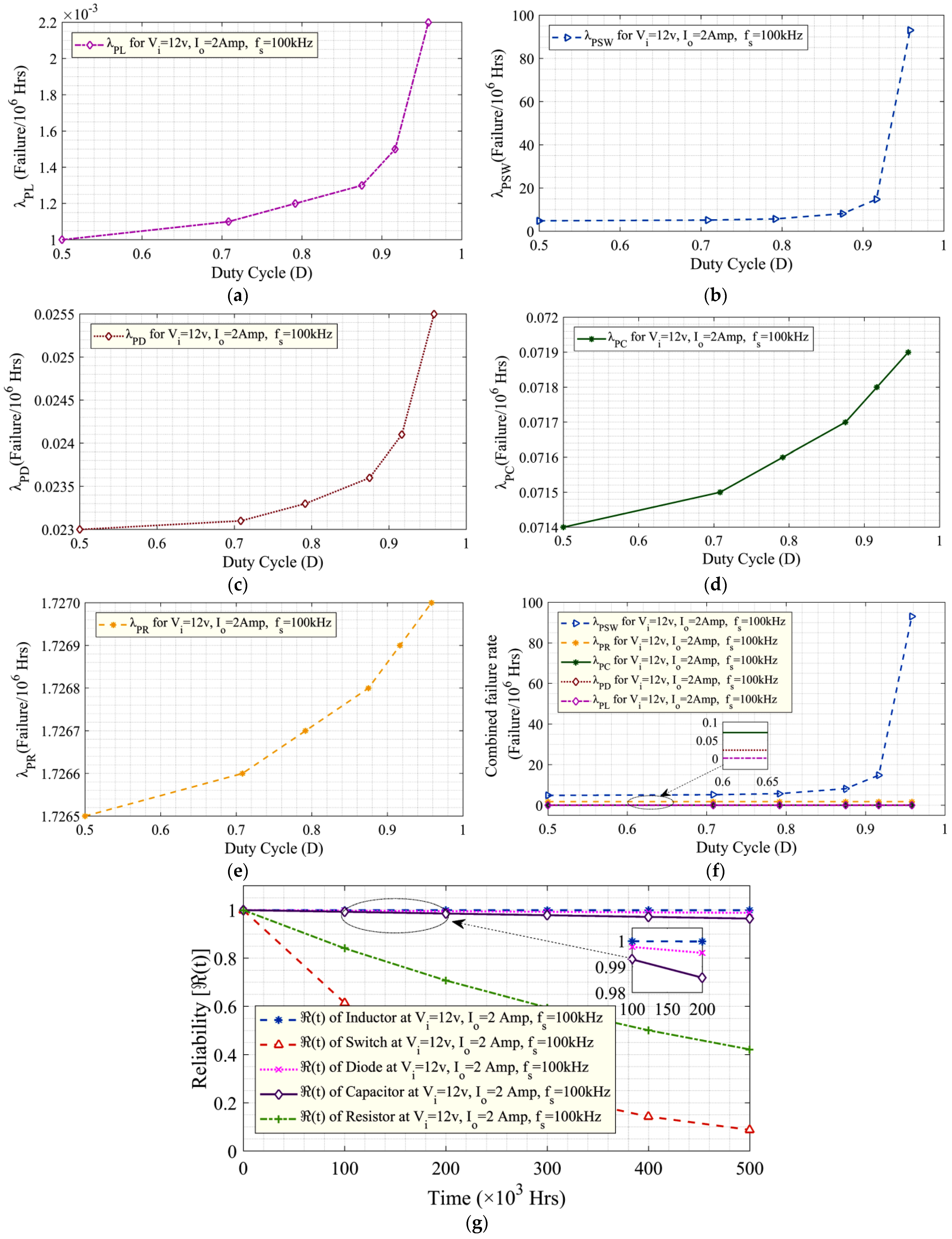
Here, Figure 16 shows the failure rates and reliability assessment outcomes of the components in a 48-watt DC-DC boost converter. Figure 16a–f showcase the failure rates of the “L”, “SW”, “D”, and “C”, respectively. In each case, it is clear that the converter’s performance also depends upon the optimal selection of the duty cycle. At a higher duty ratio, the chances of failure are high. From the analysis, it is also evident that the failure rate of inductor “L” is very small in comparison to other components in the 48-Watt transformerless DC-DC boost converter, which clearly ensures low chances of failure and long life in comparison to other components, as shown in Figure 16f.
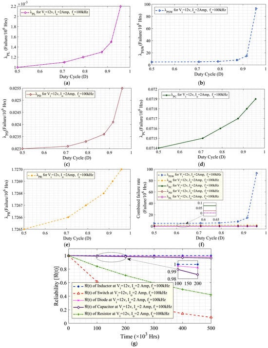
Figure 16.
Failure rates and reliability assessment outcomes of components in 48-Watt (12–24 V, 2 A, 100 kHz) transformerless DC–DC boost converter. (a) Failure rate response of inductor “L” as a function of duty cycle at 100 kHz. (b) Failure rate response of switch (MOSFET) as a function of duty cycle at 100 kHz. (c) Failure rate response of diode as a function of duty cycle at 100 kHz. (d) Failure rate response of capacitor as a function of duty cycle at 100 kHz. (e) Failure rate response of resistor as a function of duty cycle at 100 kHz. (f) Comparison of failure rates of all components as a function of duty cycle at 100 kHz. (g) Comparison of reliability for all components as a function of time.
Conversely, the research also reveals the inherent vulnerability of the switching device (MOSFET), in comparison to other components, characterized by the higher failure rate depicted in Figure 16g. Further reliability analysis was carried out using Equation (30) for each component and compared as shown in Figure 16g. The results highlight the inductor’s exceptional reliability, which is distinguished by lower failure rates in comparison to the other components. This affirms its robustness and long-term performance in practical applications.
Generalized Guidelines for the Analysis of Failure Rate and Reliability
In this paper, the failure rate and reliability analysis was carried out for active and passive components like a switch (MOSFET), diode, inductor, capacitor, etc., within a particular 48-Watt transformerless DC-DC boost converter in a comprehensive manner. In this particular section, efforts were made to provide generalized guidelines for an analysis of failure rate and reliability for active and passive components of any DC-DC converters.
- Before analyzing the failure rate and reliability of active and passive components, it is important to gather information about temperature levels. Generally, 25 °C is considered a common ambient temperature, but for office automation products, it can be considered to be 35 °C. For military and space use, it can further be considered to be more than 50 °C.
- The part failure rate should be evaluated only in “failure/106 h”.
- In failure rate analysis, the calculation of junction temperature is a crucial requirement. Sometimes. datasheets of power devices do not offer the junction-to-case thermal resistance (). Due to this, it becomes difficult to evaluate the junction temperature. In this case, the junction temperature can be calculated by considering the datasheets only with junction-to-ambient thermal resistance [.
- The base failure rate ( should be considered the same as provided in military handbooks without restricting the significant digits after the decimal point.
- The case temperature () should be calculated by taking into account the case-to-ambient thermal resistance and ambient temprature [.
- During the calculation of failure rates of inductors, the hot-spot temperature plays an important role and can be calculated as ‘’. Here, “” is the average change in temperature compared to the ambient temperature.
- It is advisable that researchers consider the selection of voltage stress “” in order to evaluate the stress factor mathematically. The voltage stress should be chosen as 0.054 (if ) and as (if 0.3 ). Here, “” is the ratio of the applied voltage to the rated voltage.
8. Conclusions
In this research paper, a comprehensive performance analysis of a 48-watt transformerless DC-DC boost converter was carried out using a PID controller. Special attention was paid to a design-oriented analysis of the inductor and the evaluation of active and passive components’ reliability. This research paper provides the complete package to researchers in terms of the design and control of a non-isolated DC-DC boost converter, with detailed dynamic modeling of its active and passive components’ reliability.
The initial simulations exposed certain shortcomings in the uncompensated boost converter, particularly in terms of overshoot, settling time, and steady-state error. At both 100 kHz and 500 kHz switching frequencies, the output current and voltage responses failed to meet the desired system response. To bridge this gap and enhance system performance, a PID controller was implemented.
To check the behavior of the linear time-invariant system and its stability, frequency response analysis was carried out using Bode plots that clearly prove that the designed system is stable. After implementing the PID controller, the results were remarkable, showcasing a significant reduction in overshoot, improved settling time, and, most importantly, outputs that met the desired current (2 A) and voltage values (24 V).
To enhance system performance, the optimal design of the magnetic element, i.e., the inductor, plays an important role. Various factors directly impact the reliability of the inductor, including the core size, core type, number of turns, wire size, etc. It is essential to thoroughly evaluate these factors for optimal reliability. These parameters are primarily influenced by variations in load, supply voltage, and load current. Improper identification of these factors may result in poor system reliability.
In this work, the “Area Product Technique” was used in terms of assessing the window area (), core cross-sectional area (), turn count (N), wire size, and core shape. The outcomes clearly demonstrate that as the load current rose, the area product window area ) proportionally rose. Further, the design analysis revealed that an elevation in the load current resulted in a reduction in the number of turns (N) and the wire size (SWG). Furthermore, the examination carried out at both 100 kHz and 500 kHz frequencies emphasizes that at higher frequencies, both the inductor size and the number of turns decreased.
As a design outcome of the inductor in a 48-watt DC-DC boost converter, the T44-26 toroidal iron powder core was chosen at 100 kHz, which exhibits an area product of and requires 18 turns with 19 SWG wires. Similarly, at 500 kHz, a T30-26 toroidal iron powder core was chosen that exhibits an area product of and requires 10 turns with 19 SWG wire.
The investigation also explored the behavior of inductor “L” as a function of the output current, input voltage, and load resistance at 100 kHz and 500 kHz frequencies. At 100 kHz, it was evident that increasing the output current decreased the inductance, while varying input voltages and load conditions demonstrated an incremental inductance trend. The research also reveals that at higher switching frequencies (500 kHz), the required inductance is low, which ultimately reduced the core size.
The behavior of inductor “L” was also examined on the basis of the power losses at 100 and 500 kHz frequencies at different operating conditions. The results clearly reveal that the inductor showed higher losses at higher load currents. At higher switching frequencies, these losses showed a very small difference in comparison to 100 kHz frequencies. One can say that inductors are less affected (in terms of power losses) at higher switching frequencies in comparison to other active components.
Further, a failure rate and reliability evaluation was carried out for active and passive components such as the switch (MOSFET), diode, capacitor, and resistor within the 48-watt boost converter. The results highlight the inductor’s exceptional reliability, which is distinguished by lower failure rates in comparison to other components. This affirms its robustness and long-term performance in practical applications. Conversely, the research also reveals the inherent vulnerability of the switching device (MOSFET), characterized by a higher failure rate and lower reliability. This research contributes to the advancement of DC-DC converter technology, providing valuable insights into comprehensive performance analysis of DC-DC boost converters with an emphasis on inductor design and component reliability. These findings will aid in the development of more efficient and dependable power conversion systems.
9. Technical Recommendations
Based on the comprehensive performance analysis, this section depicts the key recommendations that are applicable to a wide range of power electronic devices. By focusing on stability, inductor design, and component reliability, these recommendations open up the possibility for improved efficiency and lifetime across this wide range of devices.
9.1. Optimization of Inductor Design
Besides the insights gained from this research work, researchers can explore further design techniques such as the “Core Geometry Coefficient Technique (CGCT)” for inductor design by adopting different levels of operating conditions like load variations, supply voltage, load current, and frequency. In addition, investigations can be carried out for other core materials with higher saturation flux density to improve efficiency and reduce power losses.
9.2. Comparative Assessment with Other Controllers
The research can be extended by conducting a comparative analysis with other control strategies to evaluate the performance of PID controllers in different operating conditions. This will provide information about the controller’s suitability for a diverse range of power electronic applications.
9.3. Exploration of Higher Switching Frequencies
Researchers can investigate the performance of DC-DC boost converters at even higher switching frequencies in order to examine the impact on inductor design and component reliability.
9.4. Implementation of Redundancy Strategies
Researchers can carry out investigations on the implementation of redundancy strategies for components such as the MOSFET (because, according to our research, the MOSFET has poor reliability and a higher failure rate in comparison to the other power components) to improve the overall system reliability. This may involve exploring redundant configurations or fault-tolerant designs.
9.5. Consideration of Environmental Factors
This research can be extended by analyzing the impact of environmental factors on the reliability of power electronic devices. This consideration is essential for designing these devices that can withstand temperature variations, humidity, and other environmental conditions.
9.6. Expand Reliability Evaluation Using Weibull Analysis and Collaboration with Industries
The proposed reliability evaluation can be extended further by using advanced software of the Weibull theory. For this, researchers can share their research with industry partners and manufacturers to implement and validate the proposed outcomes in real-world applications. Industry collaboration ensures practical relevance and facilitates the adoption of research outcomes.
10. Economical Considerations and Recommendations
In addition to the technical insights provided, this section addresses the economic implications of the research, offering recommendations to enhance the cost-effectiveness, operation, and reliability of the 48-watt transformerless DC-DC boost converter.
10.1. Component Selection for Cost Efficiency
- During the component selection, focus should be given to both technical performance and economic feasibility.
- A thorough analysis of commercially available components can help to achieve a careful balance of performance and cost.
- According to the outcomes of this research, researchers are recommended to carefully choose components that balance the technical performance and economic feasibility.
- Researchers can use the obtained reliability data in identifying cost-effective alternatives that do not compromise the overall system performance.
- The investigation of various core materials for inductors, such as toroidal iron powder cores (T44-26 and T30-26), not only improves performance but also introduces the possibility of cost savings. Researchers can investigate alternative materials with higher saturation flux density, which balances the technical as well as cost considerations to ensure optimal resource utilization.
- Researchers can incorporate economic considerations into the component selection process. This involves conducting an in-depth assessment of commercially available alternatives, taking into account factors such as component costs, availability, and long-term reliability.
- With the help of the “Area Product Technique”, researchers can enhance their research work by not only enhancing the performance of the inductor but also minimizing the material costs.
10.2. Maintenance and Serving Strategies
- It is recommended that researchers implement a cost-effective maintenance protocol in order to minimize servicing costs. This may include preventive measures, maintenance procedures, and methods to improve the lifespan of critical components, such as the switching device (MOSFET).
- Researchers can use these reliability data to develop predictive and preventive maintenance protocols that meet the specific requirements of the identified components. The maintenance costs can be reduced by addressing potential failure points in advance, which results in a longer lifetime for the device, ultimately increasing the system’s reliability.
- Researchers can address potential issues in advance to reduce maintenance costs and increase reliability.
- To enhance the overall system reliability and reduce maintenance costs, researchers are encouraged to explore redundancy strategies for higher-failure-rate components like MOSFETs. This will further minimize the servicing costs of the converter.
10.3. Reliability Enhancement and the Total Cost of Ownership
- As the inductor exhibits exceptional reliability, efforts can be made to improve the reliability of other components, especially for the switching device. This can minimize the total costs of ownership over the device’s life cycle.
- Strategies for reliability enhancement.
- Researchers are recommended to focus on strategies that contribute to improving the reliability of specific components, particularly with lower failure rates. By selecting the critical components, the reliability of the entire system can be significantly improved by reducing the failure rate, which ultimately reduces the associated servicing costs.
- Researchers can conduct a comprehensive evaluation of servicing costs throughout the device’s life cycle, from initial manufacturing to ongoing operational and maintenance costs.
- Researchers can expand their findings by providing insights into the economic implications of reliability enhancements. By prioritizing reliability in design and maintenance strategies, researchers can offer a minimization in the total cost of ownership.
- Researchers can consider the use of cost-effective materials and design selections without reducing reliability. By optimizing the design for reliability, researchers can contribute to an economically sustainable approach that corresponds with the overall objective of reducing the total cost of ownership.
10.4. The Optimization of Design Parameters
- It is recommended that researchers consider the economic effects of design selections, especially related to the inductor.
- Evaluating the trade-offs between factors such as the core size, wire size, and number of turns can contribute to an economically optimized design.
10.5. Life Cycle Cost Analysis
- With the emerging power electronics technology, it is important to move beyond traditional cost assessments and adopt a holistic approach for life cycle cost analysis.
- Researchers can include a life cycle cost analysis to fully understand the economic implications of their power electronic devices.
These technical and economic recommendations and guidelines can facilitate researchers in terms of operational efficiency, reduced servicing costs, and increased overall economic feasibility in their future research work.
Author Contributions
Conceptualization, K.J.; methodology, K.J.; software, K.J.; validation, K.J., D.K.P. and J.M.G.; resources, J.M.G.; writing—original draft preparation, K.J.; writing—review and editing, K.J.; supervision, D.K.P. and J.M.G.; project administration, D.K.P. and J.M.G.; funding acquisition, J.M.G. All authors have read and agreed to the published version of the manuscript.
Funding
This research was funded by VILLUM FONDEN through the VILLUM Investigator Grant (No. 25920), Center for Research on Microgrids (CROM).
Institutional Review Board Statement
Not applicable.
Informed Consent Statement
Not applicable.
Data Availability Statement
Data are contained within the article.
Conflicts of Interest
The authors declare no conflicts of interest.
References
- Abbas, F.A.; Abdul-Jabbar, T.A.A.; Obed, A.A.; Kersten, A.; Kuder, M.; Weyh, T. A Comprehensive Review and Analytical Comparison of Transformerless DC-DC Converters for Fuel Cell Applications. Energies 2023, 16, 3493. [Google Scholar] [CrossRef]
- Akhtar, M.F.; Raihan, S.R.S.; Rahim, N.A.; Akhtar, M.N.; Bakar, E.A. Recent Developments in DC-DC Converter Topologies for Light Electric Vehicle Charging: A Critical Review. Appl. Sci. 2023, 13, 1676. [Google Scholar] [CrossRef]
- Hossain, S.M.S.; Haque, M.A.; Islam, R.; Mohammed, O.A. A Review of Power Electronic Converters for Electric Aircrafts. In Proceedings of the 2023 Fourth International Symposium on 3D Power Electronics Integration and Manufacturing (3D-PEIM), Miami, FL, USA, 1–3 February 2023; pp. 1–8. [Google Scholar]
- Alavi, O.; Rajabloo, T.; De Ceuninck, W.; Daenen, M. Non-Isolated DC-DC Converters in Fuel Cell Applications: Thermal Analysis and Reliability Comparison. Appl. Sci. 2022, 12, 5026. [Google Scholar] [CrossRef]
- Williams, B.W. Basic DC-to-DC Converters. IEEE Trans. Power Electron. 2008, 23, 387–401. [Google Scholar] [CrossRef]
- Mollaee, H.; Ghamari, S.M.; Khavari, F. Self-tuning regulator adaptive controller design for DC-DC Boost converter with a novel robust improved identification method. IET Power Electron. 2022, 15, 1365–1379. [Google Scholar] [CrossRef]
- Guan, Y.; Cecati, C.; Alonso, J.M.; Zhang, Z. Review of High-Frequency High-Voltage-Conversion-Ratio DC–DC Converters. IEEE J. Emerg. Sel. Top. Ind. Electron. 2021, 2, 374–389. [Google Scholar] [CrossRef]
- Dahale, S.; Das, A.; Pindoriya, N.M.; Rajendran, S. An Overview of DC-DC Converter Topologies and Controls in DC Microgrid. In Proceedings of the 2017 7th International Conference on Power Systems (ICPS), Pune, India, 21–23 December 2017; pp. 410–415. [Google Scholar]
- Musumeci, S. Energy Conversion Using Electronic Power Converters: Technologies and Applications. Energies 2023, 16, 3590. [Google Scholar] [CrossRef]
- Andrade, A.M.S.S.; Faistel, T.M.K.; Guisso, R.A.; Toebe, A. Hybrid High Voltage Gain Transformerless DC–DC Converter. IEEE Trans. Ind. Electron. 2021, 69, 2470–2479. [Google Scholar] [CrossRef]
- Rasheed, L.T. An optimal modified Elman-PID neural controller design for DC/DC Boost converter model. J. Eng. Sci. Technol. (JESTEC) 2023, 18, 880–901. [Google Scholar]
- Wang, L. PID Control System Design and Automatic Tuning Using MATLAB/Simulink; John Wiley & Sons: Hoboken, NJ, USA, 2020. [Google Scholar]
- Aseem, K.; Selva, K.S. Closed Loop Control of DC-DC Converters Using PID and FOPID Controllers. Int. J. Power Electron. Drive Syst. 2020, 11, 1323. [Google Scholar]
- Kobaku, T.; Jeyasenthil, R.; Sahoo, S.; Ramchand, R.; Dragicevic, T. Quantitative Feedback Design-Based Robust PID Control of Voltage Mode Controlled DC-DC S Converter. IEEE Trans. Circuits Syst. II Express Briefs 2020, 68, 286–290. [Google Scholar] [CrossRef]
- Zaman, M.T.; Fu, X.; Challoo, R. State-Space Average Modeling Based PID Control for Three Novel Topologies of DC-DC Boost Converter. In Proceedings of the 2022 IEEE International Women in Engineering (WIE) Conference on Electrical and Computer Engineering (WIECON-ECE), Naya Raipur, India, 30–31 December 2022; pp. 115–120. [Google Scholar] [CrossRef]
- Mclyman, C.W.M.T. Transformer and Inductor Design Handbook; CRC Press: Boca Raton, FL, USA, 2016. [Google Scholar]
- Li, X.L.; Dong, Z.; Chi, K.T.; Lu, D.D.C. Single-Inductor Multi-Input Multi-Output DC–DC Converter with High Flexibility and Simple Control. IEEE Trans. Power Electron. 2020, 35, 13104–13114. [Google Scholar] [CrossRef]
- Calderon-Lopez, G.; Scoltock, J.; Wang, Y.; Laird, I.; Yuan, X.; Forsyth, A.J. Power-Dense Bi-Directional DC–DC Converters with High-Performance Inductors. IEEE Trans. Veh. Technol. 2019, 68, 11439–11448. [Google Scholar] [CrossRef]
- Cerda, C.; Rojas, F.; Pineda, C.; Pereda, J.; Diaz, M.; Salgado, J.; Droguett, G.; Valdés, D.; Gatica, G. Inductor Design for a High-Performance DC-DC Modular Multilevel Converter. In Proceedings of the 2019 IEEE CHILEAN Conference on Electrical, Electronics Engineering, Information and Communication Technologies (CHILECON), Valparaiso, Chile, 13–27 November 2019; pp. 1–7. [Google Scholar] [CrossRef]
- Liang, D.; Shin, H.-B. Coupled Inductor Design Method for 2-Phase Interleaved Boost Converters. J. Power Electron. 2019, 19, 344–352. [Google Scholar]
- Yu, X.; Su, J.; Lai, J.; Guo, S. Analytical Optimization of Nonsaturated Thermally Limited High-Frequency Transformer/Inductor Design Considering Discreteness of Design Variables. IEEE Trans. Power Electron. 2019, 35, 6231–6250. [Google Scholar] [CrossRef]
- Radmanesh, H.; Soltanpour, M.R.; Azizkandi, M.E. Design and Implementation of an Ultra-High Voltage DC-DC Converter Based on Coupled Inductor with Continuous Input Current for Clean Energy Applications. Int. J. Circuit Theory Appl. 2021, 49, 348–379. [Google Scholar] [CrossRef]
- Mojibi, M.; Radmehr, M. Reliability evaluation of buck converter based on thermal analysis. J. Microelectron. Electron. Compon. Mater. 2018, 48, 217–227. [Google Scholar]
- Nguyen, M.H.; Kwak, S. Enhance Reliability of Semiconductor Devices in Power Converters. Electronics 2020, 9, 2068. [Google Scholar] [CrossRef]
- Rahimpour, S.; Tarzamni, H.; Kurdkandi, N.V.; Husev, O.; Vinnikov, D.; Tahami, F. An Overview of Lifetime Management of Power Electronic Converters. IEEE Access 2022, 10, 109688–109711. [Google Scholar] [CrossRef]
- MIL-HDBK-217F. Military Handbook: Reliability Prediction of Electronic Equipment; Department of Defense: Arlington, VA, USA, 1995.
- Izci, D.; Hekimoğlu, B.; Ekinci, S. A new artificial ecosystem-based optimization integrated with Nelder-Mead method for PID controller design of buck converter. Alex. Eng. J. 2022, 61, 2030–2044. [Google Scholar] [CrossRef]
- Ekinci, S.; Hekimoğlu, B.; Kaya, S. Tuning of PID Controller for AVR System Using Salp Swarm Algorithm. In Proceedings of the 2018 International Conference on Artificial Intelligence and Data Processing (IDAP), Malatya, Turkey, 28–30 September 2018; pp. 1–6. [Google Scholar] [CrossRef]
- Ersalı, C.; Hekimoğlu, B. Nonlinear model and simulation of DC-DC Buck-Boost converter using switching flow-graph method. In Proceedings of the International Informatics Congress, Kunming, China, 17–19 February 2022; pp. 15–16. [Google Scholar]
- Scirè, D.; Lullo, G.; Vitale, G. Self-Heating Induced Instability of a Non-Linear Inductor in a SMPS: A Case Study. Renew. Energy Power Qual. J. 2023, 21, 656–661. [Google Scholar] [CrossRef]
- Scirè, D.; Vitale, G.; Ventimiglia, M.; Lullo, G. Non-linear inductors characterization in real operating conditions for power density optimization in SMPS. Energies 2021, 14, 3924. [Google Scholar] [CrossRef]
- Rozenshtein, V.; Friedman, A.; Wolfus, Y.; Kopansky, F.; Perel, E.; Yeshurun, Y.; Bar-Haim, Z.; Ron, Z.; Harel, E.; Pundak, N. Saturated cores FCL—A new approach. IEEE Trans. Appl. Supercond. 2007, 17, 1756–1759. [Google Scholar] [CrossRef]
- Yahaya, E.A. Magnetic core saturation. Int. J. Eng. Sci. Math. 2013, 2, 1–6. [Google Scholar]
- Zaidi, B.; Videt, A.; Idir, N. Optimization method of CM inductor volume taking into account the magnetic core saturation issues. IEEE Trans. Power Electron. 2018, 34, 4279–4291. [Google Scholar] [CrossRef]
- Cheng, T.; Lu DD, C.; Siwakoti, Y. Electro-thermal modeling of a Boost converter considering device self-heating. In Proceedings of the 2019 IEEE 4th International Future Energy Electronics Conference (IFEEC), Singapore, 25–28 November 2019; pp. 1–6. [Google Scholar]
Disclaimer/Publisher’s Note: The statements, opinions and data contained in all publications are solely those of the individual author(s) and contributor(s) and not of MDPI and/or the editor(s). MDPI and/or the editor(s) disclaim responsibility for any injury to people or property resulting from any ideas, methods, instructions or products referred to in the content. |
© 2024 by the authors. Licensee MDPI, Basel, Switzerland. This article is an open access article distributed under the terms and conditions of the Creative Commons Attribution (CC BY) license (https://creativecommons.org/licenses/by/4.0/).

