Abstract
The discovery of the transient-surge-withstanding capability of electrochemical dual-layer capacitors (EDLCs) led to the development of a unique, commercially beneficial circuit topology known as a supercapacitor transient suppressor (STS). Despite its low component count, the new design consists of a transient-absorbing magnetic core which takes the form of a coupled inductor placed between the AC-main- and load-side varistors. With an introduction to the structural features of metal oxide varistors (MOVs), gas tubes, thyristors, and EDLCs, this research presents a frequency (S)-domain analysis of an STS circuit to accurately model the surge propagation through its coupled inductor. Transient energy distribution trends among STS components are estimated in this paper, with an emphasis on peak energies absorbed and dissipated by the various inductive, capacitive, and resistive circuit elements. Moreover, this study reveals STS transient-mode test waveforms validated by a standard lightning surge simulator with supporting simulation plots based on LTSpice numerical techniques. Both experimental and simulation results are consistent, with the analytical findings showing 90% of the peak transient propagating through the primary coil, whereas only 10% is shared into the secondary coil of the coupled inductor. In addition, it is proven that the two STS MOVs dissipate over 50% of the transient energy for a standard 6 kV/3 kA combinational surge, while the magnetic core absorbs over 20% of the energy. All test procedures conducted during this research adhere to IEEE C62.41/IEC 61000-4-5 standards.
1. Introduction
The reliability and cleanness of electrical power are key factors affecting the performance of modern electronic systems. Advancements in semiconductor technology over the years led to the development of innovative circuit designs that carry low-cost, high-precision solid-state components. The downside of such a remarkable technological revolution is the vulnerability of semiconductor-based circuitry to power quality issues. Utility mains disturbances such as voltage sags, swells, transients, over-voltages, and noise can cause data losses, equipment damage, and erroneous readings in sensitive electronic devices [1]. Overall, micro–millisecond order transients can be of higher-level magnitudes and are often responsible for the greatest voltage stress, causing high-cost damages [2]. It has been estimated that the annual cost of power quality issues in the United States is about USD 100 million to 3 billion [3], and about EUR 150 billion for the European industry [4].
1.1. Transient Protection Fundamentals and TPD Components
Given the severity and unpredictability of transients [2,5], transient protector devices (TPDs) are designed to absorb and dissipate the excessive energy detrimental to sensitive loads. An electronic system that functions optimally under 230 V starts to degrade as transient surge spikes superimpose on the AC mains flow [5,6]. Therefore, an effective TPD must absorb and dissipate the transient energy within the unit, while continually facilitating the mains electricity flow at a 50 Hz line frequency [7]. The energy content of a transient passing to the load can be evaluated using the integral of the transient voltage and current ; thus, a TPD must also be able to withstand this energy without failure [8]. Fundamentally, transient suppression occurs in two ways: series attenuation and parallel diversion. Transient stress can be serially reduced by resistors (Rs) or inductors (Ls). In particular, inductors show an elevated impedance under kHz–MHz-order transients, absorbing excessive energy passing to the load. Conversely, non-linear shunt devices such as gas discharge tubes (GDTs), metal oxide varistors (MOVs), bidirectional break-over diodes (BBDs), and capacitors (Cs) demonstrate a reduced impedance for transients (see Figure 1). Thus, these shunt TPD components divert and dissipate excessive transient energy while maintaining a safer voltage clamping across the load. Moreover, crowbar devices like thyristors (THYs) can also be useful, as described below.
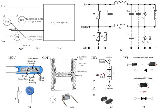
Figure 1.
Possible modes of transient occurrence and typical TPD components. (a) Different modes of voltage inputs: differential mode and common mode; (b) a typical dual-mode surge protector designed for a three-phase power system [5]; (c) metal oxide varistor (MOV) [7,9]; (d) gas discharge tube (GDT) [7,10]; (e) TVS thyristor [11]; (f) unidirectional/bidirectional TVS break-over diodes [12].
Since transient surges can appear in both differential (Live–Neutral) and common (Live–Earth and Neutral–Earth) modes (as depicted in Figure 1a), an advanced TPD must carry combinations of these series and shunt protective elements to provide versatile load protection. Figure 1b illustrates a typical dual-mode transient protector designed for a three-phase power system incorporating both modes of protection. MOVs in the circuit are the most widely used shunt TPD elements that embody a matrix of metal oxide grains in ceramic confined between two metal electrodes (see Figure 1c) [9]. Under RMS power flow, MOVs possess a high resistance, while metal oxide grains remain non-conductive; however, when transients appear across their terminals, metal oxide grains break down and start conducting at a very low resistance. This allows for transient diversion and the release of its energy through power dissipation. GDTs consist of two metallic electrodes that are separated by an air gap(s) sealed in an envelope containing an inert gas or a mixture of inert gases [10]. During high-voltage transients, the inert gas ionizes and starts to conduct, dissipating the excessive energy. Figure 1d demonstrates the interior structure and physical view of a GDT. Transient voltage suppressor (TVS) thyristors are semiconductor-based devices containing four alternating layers of p-type and n-type materials, as indicated in Figure 1e. When avalanche triggering occurs under high-voltage transients, THYs protect sensitive loads by switching to a low on-state of a few volts, thus providing a ‘crowbar’ effect with a high-current capability [11]. TVS diodes are avalanche p–n-junction-based solid-state devices that can provide either unidirectional or bidirectional protection (see Figure 1f). When two p–n junctions merge back-to-back, TVS diodes function as BBDs ( in Figure 1b) to safeguard the load from positive or negative transients appearing at the power entry point [12]. Similar to MOVs, the TVS diode is also a clamping device, which suppresses all transients above its breakdown voltage. A detailed discussion of MOV, GDT, THY, and BBD operations is beyond the scope of this paper; more information can be found in [9,10,11,12] and Table 1.

Table 1.
Characteristics comparison of TPD components.
All traditional transient suppression elements presented above possess advantages and limitations during operation. Since there is no ideal component that can fulfil all the requirements of surge suppression, a combination of components is considered when designing an effective TPD circuit. In most cases, GDTs, MOVs, and/or BBDs are coupled with series inductors and shunt capacitors for better transient filtration. Generally, all TPD components are characterized by four fundamental properties: reaction time, current handling capability, voltage clamping level, and longevity. Table 1 presents a comprehensive comparison of the characteristics of common TPD components and highlights the novelty of EDLC-type supercapacitors (SCs) applied in transient protection.
The main aim of this research is to provide an in-depth analysis of a commercialized supercapacitor-based transient suppressor (STS) using Laplace transforms and experimentally validate its transient propagation. In addition to developing S-domain models for a standard lightning surge simulator (LSS-6230) and STS circuit, this article also covers details of transient-energy distribution trends among STS components. In Section 1.2, novel aspects of using SCs in various power electronic circuits will be discussed. Section 2 will focus on comparing different chemistries of SC types, with a special emphasis on electrochemical dual-layer capacitors and their transient-withstanding capability. Frequency-domain modelling of a Noiseken LSS will be carried out in Section 3, while Section 4 provides a comprehensive analysis of STS core transient propagation using the Laplace method. Lastly, in Section 5, coupled-core energy absorption, varistor transient dissipation, and other surge losses associated with the STS circuit will be investigated.
1.2. Supercapacitors and Their Non-Traditional Applications
During the past decade, supercapacitor technologies have matured rapidly, with commercially available capacitance values ranging from 1 F to recently 100,000 F [13]. Compared to normal film-type or electrolytic capacitors (ECs), SCs offer million-times-larger capacitances, and thus posses superior energy storage capabilities over ECs. Figure 2b compares the maximum energy limits of ECs and SCs for similar canister sizes. Another remarkable benefit of SCs is the very low equivalent series resistance (ESR). Having a low ESR provides a high-current fast charge/discharge capability without excessive heating of the device [14]. This allows SCs to be used for high-power applications over batteries [15]. According to the Ragone plot shown in Figure 2a, it is clear that all SC types (EDLCs, hybrid SCs, Capa-batteries) have greater power densities than present battery technologies. However, in terms of energy densities, Li-ion, Ni-Cd, and lead-acid batteries are superior. Table 2 presents a direct comparison of the specific power/energy and charge/discharge times of batteries, supercapacitors, and capacitors. Based on these characteristics, current research trends are typically biased towards using SCs in hybrid energy-storage systems combined with batteries [16]. This could potentially boost the lifecycle of hybrid systems, with improved efficiencies compared to the ∼1000 cycles of batteries (see Table 2). Moreover, with several thousands of farad devices entering commercial markets, SCs have become commonly used as powering modules for short-to-medium-term backup systems [17]. Some automobile companies have incorporated SC banks to deliver idle power during short-term engine stops [18]. In addition, modern-day electric vehicles, aircrafts, and other rapid power portable devices utilize various types of SCs. In the recent past, a new trend has emerged of using SC banks in utility voltage stabilizer systems to provide grid support for short periods [19]. More details about SC applications are found in [13,14,15,16,17,18,19].
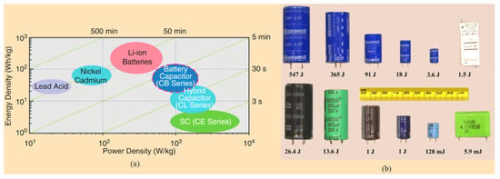
Figure 2.
Overview of battery, SC, and EC technologies: (a) Ragone plot comparing energy/power densities of batteries, SCs and ECs [20]; (b) comparison of energy storage levels of ECs, and SCs for similar canister sizes.

Table 2.
Characteristic comparison of batteries, SCs, and ECs.
Compared to these traditional applications of SCs, the University of Waikato Power Electronics group has developed a unique set of new circuit topologies, now known as SC-assisted techniques, to potentially apply this technology in various novel circuit designs. These new techniques include high-efficiency linear dc–dc converters [21], transient protectors [22], liquid-temperature-modification apparatus [23], and low-voltage LED lighting systems for DC micro-grids [24]. As mentioned previously in the introduction, this research article will provide a comprehensive analysis and experimental validation of a supercapacitor-based transient suppressor. First, the novelty of using EDLCs for transient protection applications will be discussed, with an overview of various SC chemistries.
2. Electrochemical Dual-Layer Capacitors and EDLC-based Transient Suppression
With the modern-day developments in electric-energy-storage devices, SCs have emerged as a promising candidate for high-power/longer lifecycle applications [14,15]. Especially with regard to their high power density compared to batteries and greater energy density than electrolytic capacitors (ECs), supercapacitors can bridge the gap between battery technology and conventional capacitor applications. Based on the mechanism of energy storage, SCs can be categorized into three major types [25]: (1) electrical double-layer capacitors (EDLCs), (2) pseudo-capacitors (PCs), and (3) hybrid capacitors (HCs). Of these, EDLCs were the first SCs to emerge, followed by PCs and HCs [26]. This major classification further extends into sub-types according to the chemistry of the electrodes; Figure 3 demonstrates the detailed categorization of SC types.
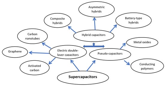
Figure 3.
Classification of supercapacitor types.
Out of the above SC types mentioned, EDLCs posses a similar capacitive arrangement to parallel plate capacitors, but due to the high surface area and extremely small charge separation distances, they exhibit much larger farad-order capacitances. Electrodes of this type are constructed using activated-carbon-based porous structures, where charge accumulation due to porosity (high surface area) is significant for better energy storage. Figure 4 illustrates the interior arrangement of electrodes and compares charged/discharged states, highlighting the distribution of charged particles (more information about EDLC charging mechanisms can be found in [27]). Notably, this greater charge-storing capability leads to a remarkably high capacitance, creating a substantial time constant in EDLC circuits. Having a larger is advantageous for withstanding transient surges, as voltage rises across EDLCs will not exceed their DC rating under such conditions [28]. Furthermore, due to the symmetrical arrangement of electrodes (Figure 4), EDLCs are applicable as reverse-polarity transients as well [29].
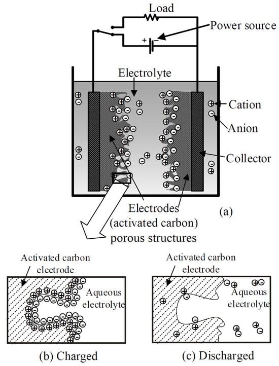
Figure 4.
Activated-carbon-based porous structures of EDLCs [30]: (a) electrode arrangement; (b) charge accumulation inside a pore; (c) a discharged state.
The pseudo-capacitor charging mechanism is governed by the Faradaic process; in such reactions, electron transfer across the two-electrode interface occurs via chemical oxidation and reduction [31]. These redox reactions can be reversible or irreversible depending on the chemical agent. Although the energy density of PCs is larger than EDLCs, the power density is much lower. Moreover, due to chemical degradation of PC electrodes (under repeated oxidation and reduction), the lifetime/cycling stability is comparably lower than EDLCs and HCs. Furthermore, when subjected to transient pulses, structure deterioration can occur in chemical electrodes of PCs; thus, their suitability for surge protection is highly limited. More details about pseudo-capacitor properties are given in [31].
Hybrid capacitors (HCs) contain a combination of EDLC and PC characteristics; these can have a greater energy density than EDLCs and a higher power density than PCs [32]. The general mechanism for construction is the hybridization of a capacitor-type electrode (activated carbon) and a battery-type chemical electrode [32]. Due to the dissimilarity of the two electrodes, HCs are considered as highly asymmetric. Notably, as transients can appear in both polarities (positive or negative transients), the usability of HCs in transient suppression circuits is extremely modest. A direct comparison of SC characteristics of EDLCs, PCs, and HCs is given in Table 3.

Table 3.
Comparison of supercapacitor type characteristics.
The overview of supercapacitor technologies provided above clearly justifies that out of EDLCs, PCs, and HCs, EDLCs are the most suitable to be used in transient protection applications. A fundamental discussion about EDLCs’ surge withstanding capabilities is presented next.
2.1. Electrochemical Dual-Layer Capacitors for Surge Suppression
The simple model we present here shows how low-DC-rated (2–4 V) EDLCs are capable of circumventing surge energy without degradation under transients. To exemplify, an circuit subjected to a rectangular surge pulse of duration T = 10 s is considered. Figure 5a illustrates the capacitance (C) of the SC, the equivalent series resistance ESR (R) of the SC, and the path resistance of the connecting wires. As indicated in Figure 5b, the SC has an extended charging curve (larger time constant) compared to an electrolytic capacitor (EC); hence, during a surge pulse, the voltage build up across a SC () is comparably small. Significantly, is typically much smaller than the rated voltage of an SC, giving it a better chance of survival under a high-voltage pulse [33]. However, in the case of a standard capacitor (EC), the developed voltage () can be higher than its rated voltage, leading to failure of the device, as shown in Figure 5c [33]. The following equations quantify the energies distributed between capacitive and resistive circuit elements during a transient pulse.
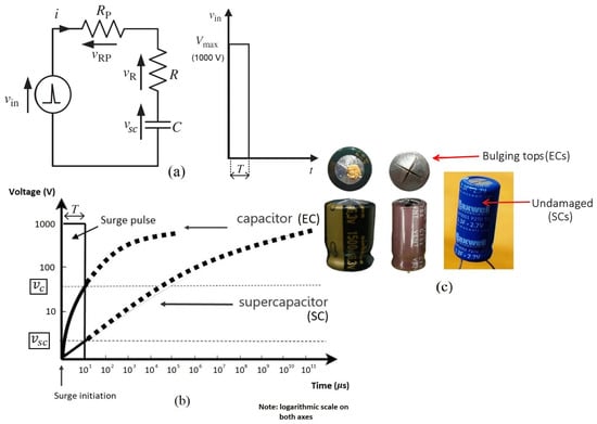
Figure 5.
RC circuit subjected to a rectangular high-voltage pulse: (a) equivalent circuit of an SC with path resistance and step voltage transient; (b) supercapacitor vs. capacitor (comparison of voltage accumulation) [34]; (c) supercapacitor vs. capacitor (comparison of physical degradation).
Equation (1) shows the energy accumulation of the SC as the voltage () across its terminals varies according to Equation (2). The surge pulse in this example has a maximum voltage () of 1000 V.
The energy dissipated in the ESR (R) of the SC due to surge current i () is given by the integral in Equation (3), where refers to the total series resistance ().
When m, , F, and s,
A key result comes from Equation (5), suggesting that a greater amount of surge energy is dissipated in ESR, while only a minor amount is sunk into the SC. This outcome further confirms how SCs can withstand transient pulses, circumventing excessive surge energy in its internal resistance. Similarly, if the circuit path resistance is significant, then a substantial amount of transient energy will be dissipated as heat across the connecting wires.
Our transient voltage tests confirm that SCs develop fairly insignificant voltages compared to ECs. A comparison of this observation is illustrated in Figure 6, with two distinct regions for the two types of capacitors. From micro-farad-level ECs to farad-level SCs, there is a substantial drop in accumulated voltages. Normal electrolytic capacitors (ECs) develop several thousands of volts when subjected to a 6 kV surge, whereas supercapacitors develop only fraction of a volt, in most cases several millivolts [35].
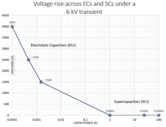
Figure 6.
Voltage development across capacitors and SCs under a standard 6 kV transient.
This remarkable surge endurance of SCs is clearly relevant in transient protection applications. However, having a low DC rating makes SCs unfit for direct application against AC mains. To address this limitation, a coupled-inductor-based topology is developed to allow SCs to be incorporated into a practical transient suppressor. Details of this development are presented next.
2.2. Supercapacitor Transient Suppressor and Its Magnetic Core
In the previous section, we explored how SCs are able to withstand transient surges without physical degradation. However, since SCs cannot be placed between live neutral terminals as a direct replacement for typical SPDs, a supercapacitor transient suppressor (STS) was developed by the Power Electronics group at the University of Waikato. An STS is a low-component-count, high-performance transient protector which utilizes a coupled inductor wound around a specially selected magnetic material. The following discussion provides an overview of the distinctive characteristics of serially placed inductors in transient protector circuits:
- For a power line transient where the surge current (i) instantaneously rises, the inductor induces a voltage proportional to that will appear as an opposing voltage barrier to the incoming surge.
- An inductor generates a high series impedance of against high-frequency transients. Compared to the 50/60 Hz power line frequency, the inductive impedance at higher-order frequencies is 400–20,000 times greater.
- Given a suitable magnetic core, an inductor can store transient energy as per , where surge-based magnetic flux is stored inside the core, safeguarding the load side.
Based on the above inductive properties, a coupled-inductor design is adopted in STS design by utilizing a toroidal core (Kool u powdered iron of = 60) with two windings, as illustrated in Figure 7b [36]. The following is a description of the topology development. As shown in Figure 7a, the two coupled windings are configured in such a way that the primary arm with 6 turns () provides a lower impedance path than the secondary arm with 28 turns () during the propagation of a surge [37]. This impedance difference allows ∼90% of the transient current to flow through the primary coil, while the inductive voltage barrier developed in the secondary arm is high enough to restrict its current share to only ∼10% [38]. In this study, detailed modelling of STS transient propagation is carried out using a Laplace transform method; theoretical predictions relating to coupled-inductor transient sharing will be presented in later sections of this paper. In addition to magnetic core inclusion, the other unique feature in STS circuit topology is the addition of a supercapacitor-based sub-circuit. A 1 high-power resistor and a 5 F SC connected serially are placed between the ends of the two inductive coils (see Figure 7a,b) to ensure that the RMS voltage across the sub-circuit never exceeds the DC rating of the SC. Therefore, any possibility of damaging the SC is prevented.
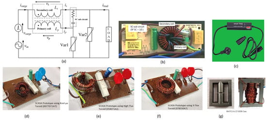
Figure 7.
STS prototypes using powdered iron and ferrite core samples: (a) STS base topology; (b) transformer core with coupled-inductor windings, SC sub-circuit and associated components; (c) commercial implementation of the STS in SMART TViQ [39]; (d) prototype using a Kool u core; (e) prototype using a high-flux core; (f) prototype using an X flux core; (g) prototype using an air-gapped EER ferrite core.
Moreover, as shown in Figure 7a, the STS circuit contains two MOVs (Var1 and Var2) to dissipate the excess surge energy while maintaining the transient voltage at a safe level. The two varistors are configured in a way that Var2 (load side) has a lower clamping than Var1. This is due to the placing of an SC sub-circuit, which develops a voltage against Var1 during transient-mode operation [40]. Overall, the combined action of the coupled inductor and the two varistors protects the critical load by storing (magnetically within the toroidal core) and dissipating (as heat) most of the transient energy. A comprehensive estimation of the surge energy distributed among various STS components will be given in this paper. In addition to the original STS circuit developed using a Kool u 0077071A7 [41] core (see Figure 7b,d), several other advancements have been accomplished using high-flux (see Figure 7e) and X flux (see Figure 7f) powdered iron magnetic materials [42]. Furthermore, in recent research given in [43], we have further improved the surge endurance and load-clamping properties of the STS by adopting an air-gapped EER ferrite core (see Figure 7g) in the coupled inductor. A comparison of the magnetic characteristics of these core samples used for prototype advancements can be found in [44].
2.3. Importance of Laplace Transforms in Transient Modelling
The coupled inductor of the STS described above is typically subjected to two distinct modes of operations: 230 V/50 Hz RMS operation and transient conditions. Unlike the steady 50 Hz condition, transients are composed of a spectrum of high frequencies [45]. Thus, inductive impedances dominate under transient surge propagation compared to a steady 50 Hz power flow. To better understand this frequency distribution, we present Fourier transforms of 6 kV and 3 kA combinational standard surges simulated in a time window of 500 s. Figure 8 demonstrates the spectrum of high frequencies corresponding to a transient starting from below 1 kHz to above 1 MHz. The DC component of the surge is removed in this figure to enhance the spectral representation of the frequencies. Considering the complex nature of rapidly varying transients, it is clear that a direct circuit analysis in the time domain will not yield accurate results for STS transient modelling; alternatively, a frequency (S)-domain analysis must be carried out. Among the various mathematical techniques available for S-domain analyses of transient waveforms in linear circuits, Laplace transforms (LTs) are regarded as one of the most convenient methods.
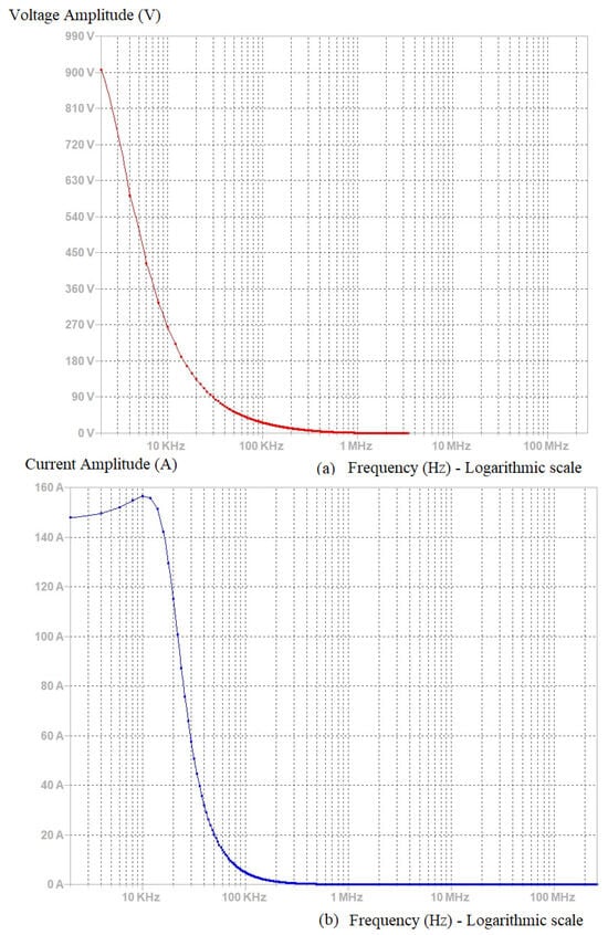
Figure 8.
Fourier transforms of 6 kV, 3 kA combinational standard surges: (a) simulated Fourier transform of a 1.2/50 µs standard voltage surge; (b) simulated Fourier transform of a 8/20 µs standard current surge.
Investigations discussed in Section 4 use the Laplace method to study transient propagation through a linearised STS circuit. First, output surge waveforms of the lightning surge simulator will be modelled using the LT as below.
3. Analysis of Lightning Surge Simulator in the S-Domain
The Noiseken lightning surge simulator (LSS-6230) was the main instrument used for standard s surge pulse generation during our experiments. The LSS-6230 is compliant with IEC61000-4-5/IEEE C62.41.2-2002 surge standards [46,47]. Therefore, in modelling the internal circuit of the LSS-6230 using the Laplace method, we first transformed all circuit parameters shown in Figure 9a into S-domain parameters, as illustrated by Figure 9b.
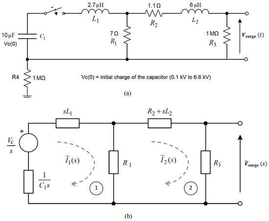
Figure 9.
Internal generation circuit of lightning surge simulator (LSS-6230) in the time and frequency domains: (a) equivalent circuit in the time domain; (b) transformed circuit network in the Laplace domain (S-domain).
LSS Internal Generation Circuit in the S-Domain
In Figure 9, the capacitor is the main energy storage element which can charge between 100 V and 6.6 kV. When the high-voltage energy is released into the wave shaping circuit consisting of inductors and and resistors , and , the standard wave shape (IEC/IEEE-defined) is produced between the open ends of the LSS [48]. In order to obtain an analytical solution for this open-circuit voltage wave, the S-domain-transformed circuit shown in Figure 9b was analysed using Kirchhoff’s laws.
Applying Kirchhoff’s voltage law for the first loop in the transformed LSS circuit:
Similarly, Kirchhoff’s voltage law for the second loop yields:
By rearranging Equation (6):
Moreover, by rearranging Equation (7):
Introducing a new parameter , Equation (9) simplifies to:
By simplifying and rearranging Equation (11), it is possible to obtain a standard S-domain representation for as:
Since LSS parameters are unique for the standard surge generation circuit, we can introduce new constant terms as , and :
Using the above constants, Equation (12) can be further simplified into:
When , and , using MATLAB Symbolic Toolbox, we can obtain the inverse transform (ilaplace) of Equation (13) to find the time-domain representation .
where = the roots of the S-domain cubic function found in Equation (13).
More information regarding the MATLAB Symbolic Toolbox commands can be found in [49]. Knowing , we can determine the open-circuit surge voltage delivered by the LSS-6230 as per Figure 9 using . For a 6 kV initial voltage ( kV) loaded to the LSS capacitor , the standard output waveform delivered by the LSS is depicted in Figure 10, with comparisons made with the Laplace analytical solution and experimental data.
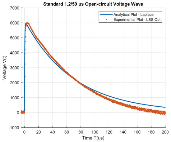
Figure 10.
Comparison of 1.2/50 s voltage wave-shape using the Laplace transform method and LSS experimental data.
According to the open-circuit LSS voltage waveforms illustrated in Figure 10, it is clear that both analytical and experimental plots show a good agreement with minor discrepancies. Both plots display a remarkable similarity to the rising half of the wave, whereas slight deviations occur during the extended falling half of the wave. This is due to experimental uncertainty and the parasitic effects of the LSS-6230’s output cables [48].
4. Laplace Validation of STS Transient Propagation
4.1. Fitting a Model for the LSS-6230 Output
The standard open-circuit voltage waveform shown above deviates from the actual peak voltage (6 kV) and wave-shape due to the impedance effects of the LSS () and connection path (). As described in [48], and the path resistance is in the order of milli-ohms. Therefore, is a significant factor for consideration when modelling the LSS output surge waveform in the presence of an STS device as the equipment under test (EUT). According to the voltage division effect shown in Figure 11, it is clear that the injected into the STS circuit is less than the actual open-circuit voltage . Hence, we fitted a model to predict this change in the surge waveform prior to the Laplace transform analysis. Based on the experimental output wave of the LSS, illustrated in Figure 12, we can identify that the 6 kV peak voltage has dropped to ∼4 kV, while there is a rapid decay in the falling edge of the waveform. Our fitted model depicted in the same plot is in good agreement with the modified mathematical constants for the double-exponential voltage wave as explained below.
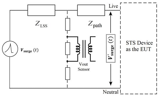
Figure 11.
Effect of the internal impedance of the LSS-6230 on transient delivery to the STS.
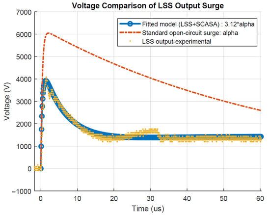
Figure 12.
Comparison of standard open-circuit surge and LSS-6230 transient output to the STS.
According to the IEEE C62.41.2 standard definition of an 1.2/50 s open-circuit voltage wave,
where the constants are , and and is the peak voltage of the waveform. Introducing a new constant , and by rearranging Equation (15),
By considering and , it is possible to express the simplified model for as:
In order to match the experimental output of the LSS, the fitted equation shown in Figure 12 must be in the form,
where , which agrees well with the reduced voltage kV when the STS is connected as the EUT to LSS output terminals. Moreover, in order to compensate for the rapid decay in the output surge, we considered a high that is 3.12 times greater than the in the original wave-shape. Standard and fitted surge models are compared with the experimental waveform in Figure 12.
To proceed further into the frequency domain analysis of the STS circuit, let us consider the Laplace transform of this modified surge wave as,
where , and with s, ss, , and kV. Equation (19) will be used in the next section for our analysis of the STS circuit in the domain. Next, we present a linearised varistor model for Var1 and Var2 in STS topology (see Figure 7a) to simplify the highly non-linear behaviour of MOVs.
4.2. Linearised Varistor Model for STS Var1 and Var2
MOVs are the most common SPD components used in surge protection circuits; these typically have a round-disc-like body or rectangular and tubular shapes. Varistors have two metal electrodes that embody a matrix of conductive zinc oxide (ZnO) or other metal oxide grains (see Figure 13a) separated by grain boundaries providing p–n junction semiconductor characteristics with highly non-linear voltage–current behaviour. Each inter-granular boundary displays a rectifying action and possesses a specific voltage barrier (breakdown voltage). As transients appear across MOV terminals exceeding this barrier voltage, metal oxide grains conduct via forming a low ohmic path to absorb and dissipate transient energy. Many layers of metal oxide grains act in a series–parallel combination between varistor electrodes to allow surge diversion at high voltages; hence, these are considered multi-junction semiconductor devices. In the STS circuit design, two MOVs (Var1 and Var2) rated for 275 V RMS conditions have been used. These MOVs have an energy rating of ≈30 J [50]. A schematic cross-sectional view of a varistor is depicted in Figure 13a. A physical view and circuit symbol of an MOV is given in Figure 13b and Figure 13c, respectively.
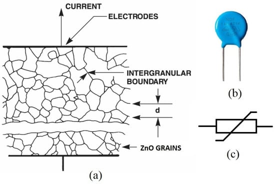
Figure 13.
Metal oxide varistor: (a) cross-sectional view; (b) physical view; (c) circuit symbol [51].
As metal oxide varistors are highly non-linear devices with a dynamic resistance () varying from milliohms to megaohms [51], we introduce a logarithmic relationship (Equation (14)) to predict the linearised states of Var1 and Var2 under transient propagation. First, we discuss the power law applied to MOVs below. The non-linear relationship between the voltage and current of an MOV is given by,
where the constants k and are unique varistor-dependent parameters; k is dependent on the device geometry and the exponent defines the degree of non-linearity [52]. For a 275 V (V20E275-Littlefuse) varistor, and [52]. Even though the characteristic takes the above form, there is a remarkable straight-line relationship specified by the manufacturers with the varistor non-linear resistance , which can be expressed as a linear function of the logarithmic current through an MOV [53]:
where the constant A = 0.035 and B and C are unit-less quantities of 2.8 and −0.95, respectively [53]. This is an empirical formula based on the magnitudes of the current/non-linear resistance (without a consideration of physical units); more information extracted from industry data sheets can be found in [51,52,53]. However, considering dimensional consistency, we divide I by 1 A and multiply the second term in Equation (14) by 1 . Equation (14) predicts the linearised states of the varistor, which are essential for our analytical work using the Laplace transform method. Figure 14 illustrates different ON and OFF resistances of the 275 V Littlefuse varistor used in the STS circuit. According to Figure 14, when:
mA →
A →
A →
A →
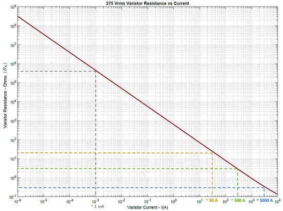

Figure 14.
Variation of 275 V (V20E275-Littlefuse) varistor resistance with current (logarithmic scale).
The calculated values for based on Equation (14) verify how the MOV shifts from M order open-circuit conditions to a highly conductive mode (Figure 14) with an ON resistance on the order of a few milli-ohms () under transient currents. Importantly, we can identify 0.3 for a standard 3 kA transient current (corresponding to a 6 kV combinational voltage wave) generated by the LSS-6230 lightning surge simulator. These linearised states of are essential for the frequency domain analysis of STS surge protectors; detailed analytical solutions are presented next.
4.3. Frequency-Domain Analysis of the Laplace-Transformed STS Circuit
In [54], we presented a permeance-based equivalent circuit model for the STS transformer core. In that model, the effect of leakage flux associated with primary and secondary core windings was indicated by means of the leakage inductances and . The magnetizing inductances and depicted in Figure 15 correspond to the magnetizing flux between the two coils. Furthermore, it was experimentally verified that the SC sub-circuit current is ∼300 A for a 6 kV/3 kA combinational transient wave. Since this current through the SC loop is fairly insignificant (∼10%) compared to the 3 kA transient, we ignored the SC sub-circuit for the convenience of a Laplace transform analysis of the STS. Figure 15 illustrates the time-domain and frequency-domain (S-domain) equivalent circuit models of the STS topology without the sub-circuit. The transformed network represented by Figure 15b is subjected to a normalized output surge waveform in the Laplace domain as discussed above. Accordingly, the fitted model (Equation (19)) for the LSS output in the presence of an STS unit is considered for this analysis.
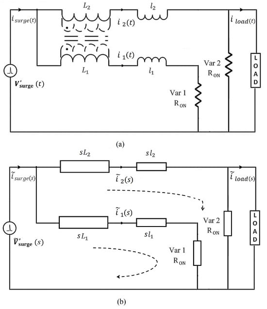
Figure 15.
Equivalent circuits of STS topology without the sub-circuit: (a) time-domain circuit; (b) frequency-domain (S-domain) circuit.
By applying Kirchhoff’s voltage law (KVL) for the first loop of the transformed STS circuit shown in Figure 15b:
Similarly, we can apply KVL for the second loop in Figure 15b:
Here, it is assumed that the load transient current (and thus ) is negligible due to the high load resistance () compared to the on resistance () of Var2. It can be calculated that for a 2 kW load powered from the 230 V mains. Since , as per the linearised varistor model (V20E275-Littlefuse) discussed in the previous section, we can assume all secondary coil current (and thus ) flows into Var2.
Isolating from Equation (22),
where the self-inductance of the primary coil according to the permeance-based circuit model described in [54]. By substituting the fitted analytical model (Equation (19)) for the LSS output waveform when the STS functions as the EUT,
Rearranging Equation (25):
To proceed further to find the inverse Laplace transform, we introduce a new constant term . Then, Equation (26) simplifies to:
Using the standard Laplace transform table found in [55] and taking the inverse transform of Equation (27), the time-domain representation of the primary current can be obtained as,
where and . Equation (28) gives an important prediction about the transient current propagation through the primary winding of the STS transformer. When , s, ssH, s, s, and s, the variation in can be plotted using MATLAB, as shown in Figure 16.
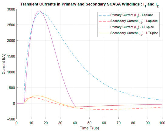
Figure 16.
Variation of primary and secondary transient currents in STS transformer for a 6 kV/3 kA combinational surge.
Furthermore, we can isolate from Equation (23),
where the self-inductance of the primary coil is according to the permeance circuit model described in [54]. By substituting the fitted analytical model’s (Equation (19)) for an LSS output waveform when the STS functions as the EUT,
Rearranging Equation (30):
To proceed further to find the inverse Laplace transform, we introduce a new constant term . Then, Equation (31) simplifies to:
Using the standard Laplace transform table in [55] and taking the inverse transform of Equation (32), the time-domain representation of the secondary current can be obtained as,
where and . Equation (33) gives an important prediction about the transient current propagation through the secondary winding of the STS transformer. When , s, ssH, s, s, and s, the variation in can be plotted using MATLAB, as shown in Figure 16.
In addition to the analytical solutions derived above, transient currents in both the primary and secondary coils, and , were numerically validated using LTSpice circuit simulations. These simulated waveforms were also plotted on the same graph (see Figure 16) to compare with the Laplace solutions. The details of the transient current division between STS coupled coils are presented next.
4.4. Validation of Transient Propagation through the STS Coupled Inductor
Notably, the transient current distribution between the two coupled windings of the STS transformer shows a considerable deviation from the AC RMS current sharing. Compared to 95%:5% (secondary:primary) RMS current division in the AC mode [54], transient propagation shows a remarkable difference, with an approximately 10%:90% sharing ratio between secondary and primary peak currents. Compared to the 50 Hz RMS condition, high-frequency transients generate greater impedances in transformer windings. Thus, the more inductive secondary coil (H), with more turns, produces a substantial impedance compared to the less inductive primary coil (H). This effect results in ∼92% (∼2.86 kA) of the total surge current passing through the primary coil, whereas only ∼8% (∼240 A) passes through the secondary coil. Figure 16 depicts how transient currents are shared among the two coupled-inductor coils using Laplace solutions and LTSpice-simulated waveforms.
In Figure 17, we present an experimental validation for transient sharing by placing high-power resistor blocks (0.21 ) in series with the primary and secondary STS windings (see Figure 17b). In order to conduct transient testing, a NoiseKen LSS-6230 (NoiseKen Laboratories, Sagamihara City, Japan) lightning surge simulator, high-voltage probes (Tektronix P6015 A, Tektronix Inc., Beaverton, OR, USA), and an isolated-channel oscilloscope (Tektronix TPS2014, Tektronix Inc., Beaverton, OR, USA) were used as the main instruments. With the insertion of small resistor blocks for transient monitoring, our measurement system yielded deviated results compared to the analytical and simulated waveforms illustrated in Figure 16. Figure 17c demonstrates the oscilloscope voltage waveforms captured across the high-power resistor blocks. By dividing these peak voltages by 0.21 , peak current sharing through coupled-inductor windings can be determined ( and ). This discrepancy in the test results is due to the impedance effects of the two resistor blocks placed in line with the STS transformer windings. It was experimentally challenging to capture rapidly varying transient currents (due to high magnitudes and kHz-order frequencies) with the available test facilities. However, we verified the Laplace transform predictions using LTSpice numerical simulations, as demonstrated in Figure 16, and these were in agreement according to peak current values, though a mismatch in wave shapes is seen for the primary current during the falling edge. This mismatch is due to the non-linearity of Var1 (connected to the primary coil) which was assumed to be at a linear ON state of 0.3 . Furthermore, since Var1 is undergoing a highly non-linear transition from a conductive ON state to an OFF state at the falling edge of the primary current , it can be seen that the analytical prediction for deviates from the simulation during this falling half. However, considering the mathematical complexity of varistor behaviour, our main aim of the Laplace analysis was to validate peak current divisions in the STS coupled inductor. The LTSpice circuit models used for the numerical simulations of LSS and STS equivalent circuits are given in Figure 18.
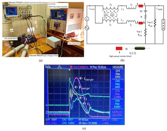
Figure 17.
Experimental setup and test waveforms for STS operation under a transient of 6 kV/3 kA: (a) STS circuit under transient testing using LSS-6230; (b) measurement system for monitoring coupled-inductor currents using high-power resistors; (c) test waveforms for primary and secondary transient currents under a 6 kV/3 kA combined surge and STS Var2 clamping.
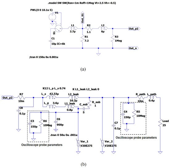
Figure 18.
LTSpice simulation circuits: (a) LSS-6230 surge simulator circuit used in the simulations; (b) equivalent circuit of the STS topology simulated in LTSpice (including the X- and Y-EMI filtering capacitors (C6, C7, and C8), oscilloscope probe parameters, and path impedance characteristics).
5. Estimation of Transient Energy Distribution in STS Circuit Components
5.1. Energy Absorbed by the Magnetic Core
As described previously in Section 2, the STS magnetic core comprises two coupled windings wound to a powdered iron toroid. Therefore, the core absorbs and stores surges in the form of inductive energy during transient propagation. The primary and secondary coils of the STS coupled inductor posses self-inductances on the microhenry order; however, as both coils share high-magnitude surge currents, energy absorption by the core becomes significant. In the following discussion, we quantify the peak energies stored by the two magnetic coils.
The peak energy stored in the primary coil with a self-inductance of H carrying a surge current of 2.86 kA is
Similarly, the peak energy stored in the secondary coil of with a self-inductance of H and carrying a surge current of 240 A is
Given the above calculation for the peak energies (further confirmed by Figure 19), it is clear that the total surge energy absorbed by the STS magnetic core is ∼18 J (). For a standard 6 kV/3 kA surge, which delivers a total energy of ∼81 J [56], the percentage of inductive energy absorption is ∼22%. It is important that during transient propagation, the Kool u powdered iron core stays under its magnetic saturation limit. In separate research [44], we evaluated the surge-related magnetic flux for a Kool u toroid and compared STS performance levels with other core types that have better magnetic saturation. Apart from the core absorption, the STS circuit also dissipates a significant share of the surge energy in the two varistors Var1 and Var2. In the next section, varistor energy dissipation is discussed.
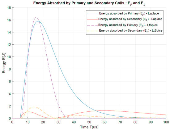
Figure 19.
Variation in transient energy absorbed by primary and secondary windings of the STS transformer (under a 6 kV/3 kA combinational surge).
5.2. Energy Dissipation in Varistors
In Section 4.3, it was theoretically proven that the transient currents are divided between primary and secondary windings of the STS core based on the inductive impedance of the two coils. According to Figure 16, the less inductive primary coil had ∼92% of the total surge current, whereas the secondary had ∼8%. Corresponding to this transient division, the heat dissipation by Var1 and Var2 (connected to primary and secondary coils, respectively) shows a similar pattern, as most of the surge energy is dissipated across Var1. Figure 20 depicts the heat dissipation across Var1 and Var2 over a 100 s period under a 6 kV/3 kA transient. According to Figure 20a, Var1 exhibits a peak power of ∼2.3 MW, whereas Var2 exhibits ∼0.1 MW of peak dissipation. However, to obtain a better understanding, we plotted the energy dissipation in Figure 20b. Both the power and energy variations shown below were obtained using LTSpice simulations; details about the simulated circuit models are given in Figure 18. Notably, ∼40 J of peak surge energy is lost via Var1 as heat; this is, in comparison, 20 times greater than the ∼2 J peak dissipation of Var2. Compared to a standard 6 kV/3 kA surge, which delivers a total energy of ∼81 J, STS Var1 dissipation is ∼49% of ; thus it experiences the greatest transient stress over all other STS circuit components. Conversely, the ∼2 J surge dissipation across Var2 is only ∼2.5% of , meaning that it is not likely to fail under repeated surge pulses and provides reliable protection of the connected load.
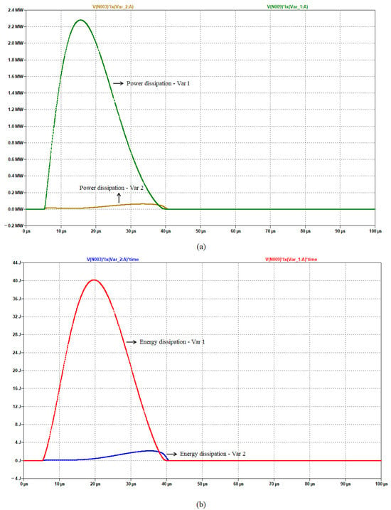
Figure 20.
Heat dissipation across Var1 and Var2 of an STS circuit for a 6 kV/3 kA combinational surge: (a) power dissipation plot; (b) energy dissipation plot.
The resistive elements () of the two MOVs facilitate the surge energy dissipation, as described above, and cool down immediately to recover back to their mega-ohm level open-condition prior to the propagation of the next surge. In UL-1449 3rd edition testing, we set these time intervals between repetitive surges to either 1 min or 30 min (more information about UL-1449 testing can be found in [57]). However, with the heat dissipations due to repetitive surge pulses, internal degradation of zinc oxide granular layers occurs, resulting a reduction in the MOV’s lifetime. In addition to finding the peak energy dissipation presented above, we evaluated the following integrals to determine the average heat stress across the two varistors.
The average surge energy dissipation across Var1 is given by,
where s, , and is the primary coil surge current determined using Laplace transforms as per Equation (28). Based on MATLAB calculations, the above integral is evaluated as,
Similarly, the average surge energy dissipation across Var2 is given by,
where is the secondary coil surge current as determined using Laplace transforms in Equation (33). Using MATLAB, the above integral is evaluated as,
According to these calculations, it is clear that even for a ∼40 J peak dissipation, Var1 showed a ∼18 J average energy. Conversely, Var2 exhibited an average of ∼0.8 J for its maximum ∼2 J dissipation. This proves how both varistors have a reduced heat stress as the transient currents propagate rapidly within a few microseconds. However, it must be noted that thermal degradation occurs in MOVs due to repetitive surge pulses; hence, failure can occur in the long run. More information about MOV degradation patterns can be found in [58]. Next, we aim to estimate the energy distribution within the supercapacitor (SC) sub-circuit of the STS circuit.
5.3. Energy Dissipated by the SC Sub-Circuit
The SC sub-circuit in the original STS design was placed between the primary and secondary coils of the coupled inductor. As described previously in Section 2.2 (see Figure 7), the sub-circuit consists of a 1 high-power resistor and a 5 F supercapacitor. Due to the milli-ohm order ESR of the SC, most surge dissipation within the sub-circuit happens through the 1 resistor. Figure 21 illustrates how heat dissipation varies across 1 resistor during the transient propagation.
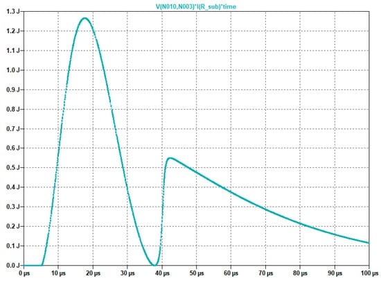
Figure 21.
Heat dissipation across high-power resistor in STS sub-circuit for a 6 kV/3 kA combinational surge.
According to this LTSpice simulation, we can identify the maximum energy loss as ∼1.3 J, which is then followed by a secondary peak of ∼0.6 J. Compared to the input transient energy of 81 J injected into the STS circuit, the loss in the 1 high-power resistor is relatively insignificant, at only ∼1.6% of . However, the SC sub-circuit is mainly used as an electromagnetic interference (EMI) filter inside the STS topology to provide better filtration of transients. Furthermore, in Section 2.2, we explained how useful the sub-circuit is in placing a supercapacitor between the coupled-inductor coils without exceeding its rated voltage under AC RMS operation. In the next section, a summary of the surge energies distributed among various STS circuit components will be presented.
5.4. Additional Surge Losses and Comparison of Transient Energy Distribution Patterns
Given the detailed energy estimation for various inductive and resistive elements in the STS circuit, in this section, we present a comparison of surge energy distributions using a percentage analysis. For this comparison, we have considered that the peak energy of a standard 1.2/50 s, 6 kV/3 kA combinational surge is ∼81 J [56]. Table 4 demonstrates the transient absorptions/dissipations associated with the magnetic core, metal oxide varistors, and the high-power resistor of the STS. The coupled inductor core comprises primary and secondary windings which store ∼16 J and ∼2 J, respectively, and this can be approximated to 20% and 2.5% of the total surge energy input. Notably, Var1, connected to the primary coil, shows the highest heat dissipation at ∼40 J, which is ∼49% of the total transient energy. Conversely, Var2, which has a lower current flow than Var1, dissipates only 2 J, indicating that Var2 experiences the lowest transient stress, protecting the sensitive load. Furthermore, as described in the previous section, the 1 high-power resistor in the SC sub-circuit dissipates ∼1.6% of the surge, assisting the supercapacitor to function as an EMI filter. Interestingly, the rest of the transient energy is wasted in the path resistances of the connecting wires and leads. We measured the total path resistance () as ∼0.2 , and when the 3 kA peak surge current flows through the connecting wires, it dissipates nearly 18 J as heat (Table 4). A simplified calculation is shown below.

Table 4.
Comparison of peak surge energy distribution in STS components for a 6 kV/3 kA combinational surge.
When the transient current () peak of 3 kA occurs at 10 s,
This ∼18 J is an effective surge loss that reduces the transient stress on the surge protector under operation. As a percentage, this path dissipation corresponds to ∼22% of the total surge energy, proving to be significant even for a relatively small ∼0.2 path resistance. Overall, it is clear that our total energy estimation for various inductive and resistive circuit elements in STSs is comparable to the ∼81 J of the input combinational surge.
6. Conclusions
With the novel application of EDLC supercapacitors for transient suppression, a coupled-inductor-based circuit topology called an STS was designed and introduced to the commercial market as Smart-TViQ. Given the low component count and its advanced level of transient filtration, the STS technique was superior to most other commercial designs, withstanding UL-1449 surge immunity tests. Based on the Laplace transform method, this paper presented in-depth modelling of the STS magnetic core and associated circuit components to predict its transient propagation and surge energy distribution. According to the analytical, experimental, and simulation results, it was revealed that ∼90% of the transient current propagates through the core primary winding, whereas only ∼10% is shared into the secondary side. Frequency-domain models developed for the Noiseken LSS-6230 lightning surge simulator also yielded accurate predictions of the open-circuit surge waveforms, consistent with the experimental results.
To envisage the MOV’s non-linear behaviour in the STS circuit, a linearized varistor model was introduced, relating the MOV ON resistance with its current in logarithmic form. According to theory, the 275 V varistor resistance dropped to as low as ∼0.3 under a standard 3 kA transient, whereas a steady mega-ohm resistance was maintained under 230 V, 50 Hz RMS conditions. Moreover, this study unveiled surge energy distribution patterns among various STS components, where it was found that a significant share (∼49%) of the energy is dissipated in Var1 compared to ∼2.5% dissipation in Var2. Coupled windings of the magnetic core showed a substantial 22.5% energy absorption, minimizing the transient stress on both varistors. Notably, the path resistances of the STS circuit wires revealed an effective 18 J energy dissipation out of the ∼81 J input of standard combinational transient.
Funding
This research received no external funding.
Institutional Review Board Statement
Not applicable.
Informed Consent Statement
Not applicable.
Data Availability Statement
Data are contained within the article.
Conflicts of Interest
The author declares no conflict of interest.
Abbreviations
The following abbreviations are used in this manuscript:
| AC | Alternating Current |
| EUT | Equipment Under Test |
| EC | Electrolytic Capacitor |
| EDLC | Electrochemical Dual-Layer Capacitor |
| EMI | Electromagnetic Interference |
| ESR | Equivalent Series Resistance |
| HC | Hybrid Capacitor |
| LSS | Lightning Surge Simulator |
| LT | Laplace Transform |
| NLD | Non-Linear Device |
| GDT | Gas Discharge Tube |
| BBD | Bidirectional Break-over Diode |
| MOV | Metal Oxide Varistor |
| PC | Pseudo Capacitor |
| RMS | Root Mean Square |
| SC | Supercapacitor |
| SMART TViQ | Commercial Implementation of STS Technique |
| STS | Supercapacitor Transient Suppressor |
| THY | Thyristor |
| TPD | Transient Protector Device |
| TVS | Transient Voltage Suppressor |
| Var1 and Var2 | Varistor 1 and Varistor 2 of the STS Circuit |
References
- Dranetz, T. The Dranetz Field Handbook for Power Quality Analysis; Dranetz Technologies Incorporated: Brockton, MA, USA, 2020. [Google Scholar]
- Seksena, S.B.L.; Kaustuv, D. Fundamentals of Electrical Engineering; Cambridge University Press: Cambridge, UK, 2018. [Google Scholar]
- Fuchs, E.F.; Masoum, M.A.S. Power Quality in Power Systems, Electrical Machines, and Power-Electronic Drives, 3rd ed.; The Academic Press: Boston, MA, USA, 2023. [Google Scholar]
- Targosz, R.; Manson, J. Pan-European power quality survey. In Proceedings of the 2017 9th International Conference on Electrical Power Quality and Utilisation, Barcelona, Spain, 9–11 October 2017; pp. 1–6. [Google Scholar] [CrossRef]
- Barnes, J.R. (Ed.) Transient Suppressors and Surge Suppressors. In Robust Electronic Design Reference Book; Springer: Berlin/Heidelberg, Germany, 2019. [Google Scholar]
- Joffe, E.B.; Lock, K. Grounds for Grounding: A Handbook from Circuits to Systems; John Wiley: Chichester, UK, 2023. [Google Scholar]
- IEEE Std C62.42.0-2016; IEEE Guide for the Application of Surge-Protective Components in Surge-Protective Devices and Equipment Ports—Overview. IEEE: New York, NY, USA, 2017; pp. 1–66. [CrossRef]
- Kularatna, N.; Ross, A.S.; Fernando, J.; James, S. Design of Transient Protection Systems; Elsevier: Amsterdam, The Netherlands, 2019; pp. 1–16. [Google Scholar]
- IEEE Std C62.42.2–2022; IEEE Guide for the Application of Surge-Protective Components in Surge-Protective Devices and Equipment Ports—Part 2: Metal- Oxide Varistors (MOVs). IEEE: New York, NY, USA, 2022; pp. 1–60. [CrossRef]
- IEEP62.42.1/D3; IEEE Draft Guide for the Application of Surge-Protective Components in Surge Protective Devices and Equipment Ports—Part 1: Gas Discharge Tubes (GDTs). IEEE: New York, NY, USA, 2014; pp. 1–40.
- HBD855/D, 2006:11; Thyristor theory and design considerations. On Semiconductor Publications: Santa Clara, CA, USA, 2006.
- TVS Diodes. Littelfuse Corporation. 2023. Available online: https://www.littelfuse.com/products/tvs-diodes (accessed on 10 July 2023).
- Adedoja, O.S.; Sadiku, E.R.; Hamam, Y. An Overview of the Emerging Technologies and Composite Materials for Supercapacitors in Energy Storage Applications. Polymers 2023, 15, 2272. [Google Scholar] [CrossRef] [PubMed]
- ESD-SCAP Catalogue; SAMWHA Capacitor Co. Ltd.: Yongin-si, Republic of Korea, 2022.
- Kularatna, N.; Gunawardane, K. Energy Storage Devices for Renewable Energy-Based Systems: Rechargeable Batteries and Supercapacitors; Elsevier Academic Press: Waltham, MA, USA, 2021. [Google Scholar]
- Reddy, R.M.; Das, M.; Chauhan, N. Novel Battery-Supercapacitor Hybrid Energy Storage System for Wide Ambient Temperature Electric Vehicles Operation. In IEEE Transactions on Circuits and Systems II: Express Briefs; IEEE: New York, NY, USA, 2023; Volume 70, pp. 2580–2584. [Google Scholar] [CrossRef]
- Yin, Z.; Han, M.; Du, Y.; Zhang, Z. A practical approach for ride through of super capacitor energy storage based ASD system. In Proceedings of the IEEE Transmission Distribution Conference & Exhibition, Dallas, TX, USA, 21–24 May 2006; pp. 744–746. [Google Scholar]
- Automotive Applications for Supercapacitors and Ultra-Capacitors: Cap-XX (2021) CAP. Available online: https://www.cap-xx.com/applications/auto/ (accessed on 10 July 2023).
- Kumar, S.; Agrawal, A.; Gupta, R. Power Balance for WTG-Solar PV Fed DC Microgrids with Battery and Supercapacitor Support. In Proceedings of the 2018 IEEE International Conference on Power Electronics, Drives and Energy Systems (PEDES), Chennai, India, 18–21 December 2018; pp. 1–6. [Google Scholar] [CrossRef]
- Kularatna, N.; Jayananda, D. Supercapacitor-Based Long Time-Constant Circuits: A Unique Design Opportunity for New Power Electronic Circuit Topologies. IEEE Ind. Electron. Mag. 2020, 14, 40–56. [Google Scholar] [CrossRef]
- Gunawardane, K.; Kularatna, N. Supercapacitor-Assisted Low dropout Regulator Technique: A new design approach to achieve highefficiency linear DC-DC converters. IET Power Electron. 2017, 11, 229–238. [Google Scholar] [CrossRef]
- Fernando, J.; Kularatna, N.; Silva, S.; Silva Thotabaddadurage, S. Supercapacitor assisted surge absorber technique: High performance transient surge protectors for consumer electronics. IEEE Power Electron. Mag. 2022, 9, 48–60. [Google Scholar] [CrossRef]
- Gurusinghe, N. Supecapacitor-Assisted Temperature Modification Apparatus (SCATMA) and Fast Supercapacitor Charger. Ph.D.Thesis, University of Waikato, Hamilton, New Zealand, 2016. [Google Scholar]
- Udathenne Gedara, D.U.K.J. Supercapacitor assisted LED (SCALED) Converter Technique for Solar Powered DC-Microgrids. Ph.D.Thesis, The University of Waikato, Hamilton, New Zealand, 2020. [Google Scholar]
- Raza, W.; Ali, F.; Raza, N.; Luo, Y.; Kim, K.; Yang, J.; Kumar, S.; Mehmood, A.; Kwon, E. Recent advancements in supercapacitor technology. Nano Energy 2018, 52, 441–473. [Google Scholar] [CrossRef]
- Lamba, P.; Singh, P.; Singh, P.; Singh, P.; Bharti; Kumar, A.; Gupta, M.; Kumar, Y. Recent advancements in supercapacitors based on different electrode materials: Classifications, synthesis methods and comparative performance. J. Energy Storage 2022, 48, 103871. [Google Scholar] [CrossRef]
- Conway, B.E. Electrochemical Supercapacitors: Scientific Fundamentals and Technological Applications; Springer: New York, NY, USA, 2013. [Google Scholar]
- Silva Thotabaddadurage, S.U.; Kularatna, N.; Steyn-Ross, D.A. Optimization of Supercapacitor Assisted Surge Absorber (SCASA) Technique: A New Approach to Improve Surge Endurance Using Air-Gapped Ferrite Cores. Energies 2021, 14, 4337. [Google Scholar] [CrossRef]
- Kularatna, N.; Fernando, J.; Pandey, A.; James, S. Surge capability testing of supercapacitor families using a lightning surge simulator. IEEE Trans. Ind. Electron. 2011, 58, 4942–4949. [Google Scholar] [CrossRef]
- Silva Thotabaddadurage, S.U. Permeance Based Modelling, Design and Optimization of Supercapacitor Assisted Surge Absorber (SCASA). Ph.D.Thesis, The University of Waikato, Hamilton, New Zealand, 2021. Available online: https://hdl.handle.net/10289/14602 (accessed on 1 January 2020).
- Lu, Q.; Chen, J.G.; Xiao, J.Q. Nanostructured electrodes for high performance pseudo-capacitors. Angew. Chem. Int. Ed. 2013, 52, 1882–1889. [Google Scholar] [CrossRef] [PubMed]
- Muzaffar, A.; Basheer, M.; Deshmukh, K.; Thirumalai, J. A review on recent advances in hybrid supercapacitors: Design, fabrication and applications. Renew. Sustain. Energy Rev. 2019, 101, 123–145. [Google Scholar] [CrossRef]
- Fernando, J. Supercapacitor-Assisted Surge Absorber (SCASA) and Supercapacitor Surge Modelling. Ph.D. Thesis, The University of Waikato, Hamilton, New Zealand, 2016. [Google Scholar]
- Udayanga, S.T.S.; Kokuhennadige, S.; Fernando, J.; Kularatna, N.; Steyn-Ross, D.A. Supercapacitor assisted surge absorber (SCASA) technique: Selection of magnetic components based on permeance. In Proceedings of the 2021 IEEE Applied Power Electronics Conference and Exposition (APEC), Phoenix, AZ, USA, 14–17 June 2021; pp. 2299–2304. [Google Scholar] [CrossRef]
- Kularatna, N.; Fernando, J.; Pandey, A. Surge endurance capability testing of supercapacitor families. In Proceedings of the 36th Annual IECON 2010 Conference of IEEE Industrial Electronics Society, 7–10 November 2010; pp. 1858–1863. [Google Scholar]
- Udayanga, S.T.S.; Kularatna, N.; Steyn-Ross, D.A. Permeance based model for the coupled-inductor utilized in the supercapacitor assisted surge absorber (SCASA) and its experimental validation. In Proceedings of the 2020 2nd IEEE International Conference on Industrial Electronics for Sustainable Energy Systems (IESES), Cagliari, Italy, 1–3 September 2020; pp. 267–272. [Google Scholar] [CrossRef]
- Sadeeshvara, S.T.; Kularatna, N.; Steyn-Ross, D.A. Investigating the impact of ferrite magnetic cores on the performance of supercapacitor assisted surge absorber (SCASA) technique. In Proceedings of the 2019 IEEE 28th International Symposium on Industrial Electronics (ISIE), Vancouver, BC, Canada, 12–14 June 2019; pp. 130–135. [Google Scholar] [CrossRef]
- Silva Thotabaddadurage, S.U.; Kularatna, N.; Steyn-Ross, D.A. Permeance Based Design and Analysis of Supercapacitor Assisted Surge Absorber for Magnetic Component Selection. IEEE Trans. Ind. Electron. 2023, 70, 3593–3603. [Google Scholar] [CrossRef]
- Thor Technologies—STViQ/3 SMART TViQ. 2018. Available online: https://www.thortechnologies.com.au/product/stviq3/ (accessed on 22 April 2023).
- Fernando, J.; Kularatna, N. A supercapacitor based enhancement technique for stand-alone surge protection circuits. In Proceedings of the 2013 IEEE International Symposium on Industrial Electronics, Taipei, Taiwan, 28–31 May 2013; pp. 1–6. [Google Scholar] [CrossRef]
- Magnetics Inc. Kool Mu Powder Cores, Mag-inc.com. 2023. Available online: https://www.mag-inc.com/products/powder-cores/kool-mu-cores (accessed on 26 January 2023).
- Magnetics Inc. ‘2021 Magnetics Powder Core Catalogue’, Mag-inc.com. 2021. Available online: https://www.maginc.com/Design/Technical-Documents/Powder-Core-Documents (accessed on 28 January 2023).
- Thotabaddadurage, S.U.S.; Kularatna, N.; Steyn-Ross, D.A. Importance of Leakage Magnetic Field and Fringing Flux in Surge Protector Design. IEEE Trans. Ind. Appl. 2023, 59, 289–299. [Google Scholar] [CrossRef]
- Silva, S.; Kularatna, N.; Steyn-Ross, D.A. Magnetic Design Aspects of Coupled-Inductor Topologies for Transient Suppression. Electronics 2023, 12, 246. [Google Scholar] [CrossRef]
- Su, Q. Electromagnetic Transients in Transformer and Rotating Machine Windings; Information Science Reference: Kyiv, Ukraine, 2013. [Google Scholar]
- IEC 61000-4-5; Electromagnetic Compatibility (EMC)—Art 4–5: Testing and Measurement Techniques—Surge Immunity Test. International Electrotechnical Commission: Geneva, Switzerland, 2014.
- IEEE Std C62.41.2-2002; IEEE Recommended Practice on Characterization of Surges in Low-Voltage (1000 V and Less) AC Power Circuits. IEEE: New York, NY, USA, 2003.
- NoiseKen Laboratories. Lightning Surge Simulator LSS-6230 Series; Technical Report; compliant with IEC61000-4-5 Edition-3 requirements; NoiseKen Laboratory Co. Ltd.: Sagamihara, Japan, 2014. [Google Scholar]
- MathWorks Inc. Symbolic Math Toolbox for Use with MATLAB: User’s Guide. In MATLAB Handbooks; MathWorks, Incorporated: Natick, MA, USA, 2022. [Google Scholar]
- Littelfuse Inc. Ultra MOV Varistor Series: Radial Lead Varistors. 2020. Available online: https://www.littelfuse.com/~/media/electronics/datasheets/varistors/ (accessed on 28 December 2022).
- AN9767.1; Littelfuse Varistors—Basic Properties, Terminology and Theory. Littlefuse Co-operation: Chicago, IL, USA, 1999.
- Chen, H.; Du, Y. A comprehensive study on the non-linear behaviour of metal oxide varistors. In Proceedings of the 2016 33rd International Conference on Lightning Protection (ICLP), Estoril, Portugal, 25–30 September 2016; pp. 1–5. [Google Scholar]
- Maytum, M. There’s an “R” in “VARISTOR”. 2020. Available online: https://incompliancemag.com/article/theres-an-r-in-varistor/ (accessed on 24 November 2022).
- Bossche, A.; Valchev, V. Inductors and Transformers for Power Electronics; Taylor & Francis: New York, NY, USA, 2018. [Google Scholar]
- Schiff, J.L. The Laplace Transform: Theory and Applications. Undergraduate Texts in Mathematics; Springer: New York, NY, USA, 2013. [Google Scholar]
- Alonzo, R.J. Electrical Codes, Standards, Recommended Practices and Regulations: An Examination of Relevant Safety Considerations; Elsevier Science: Amsterdam, The Netherlands, 2009. [Google Scholar]
- UL 1449; UL Standard for Surge Protective Devices, 5th ed. Underwriters Laboratories Inc.: Brooklyn, IL, USA, 2021.
- Khanmiri, D.T.; Ball, R.; Lehman, B. Degradation Effects on Energy Absorption Capability and Time to Failure of Low Voltage Metal Oxide Varistors. IEEE Trans. Power Deliv. 2017, 32, 2272–2280. [Google Scholar] [CrossRef]
Disclaimer/Publisher’s Note: The statements, opinions and data contained in all publications are solely those of the individual author(s) and contributor(s) and not of MDPI and/or the editor(s). MDPI and/or the editor(s) disclaim responsibility for any injury to people or property resulting from any ideas, methods, instructions or products referred to in the content. |
© 2023 by the author. Licensee MDPI, Basel, Switzerland. This article is an open access article distributed under the terms and conditions of the Creative Commons Attribution (CC BY) license (https://creativecommons.org/licenses/by/4.0/).