
Combined Treatment of Parts Produced by Additive Manufacturing Methods for Improving the Surface Quality


Abstract
1. Introduction
- -
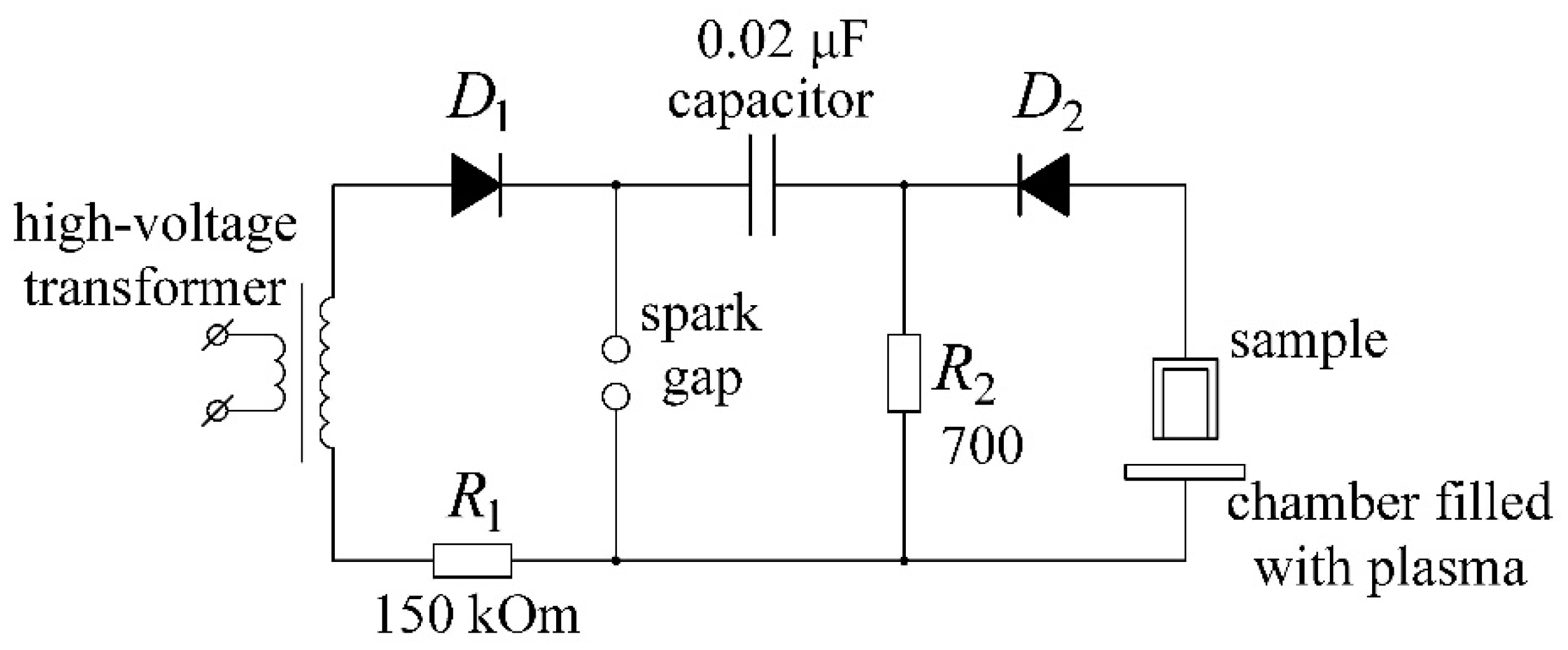
- explosive ablation of surface protrusions when high-voltage pulses are applied to a part immersed in plasma;
- -
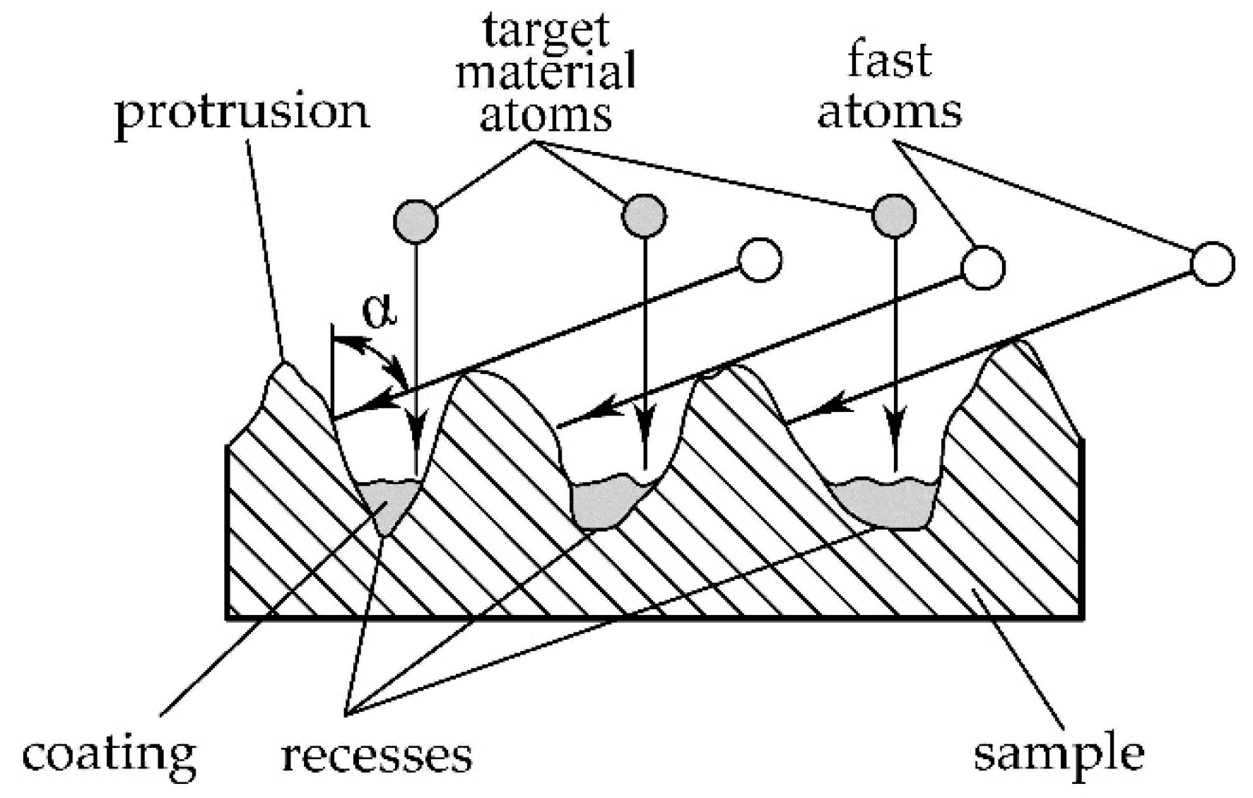
- polishing with a concentrated beam of fast neutral argon atoms at a large angle of incidence on the part surface;
- -
- magnetron deposition on the part of a coating assisted by fast argon atoms.
2. Materials and Methods
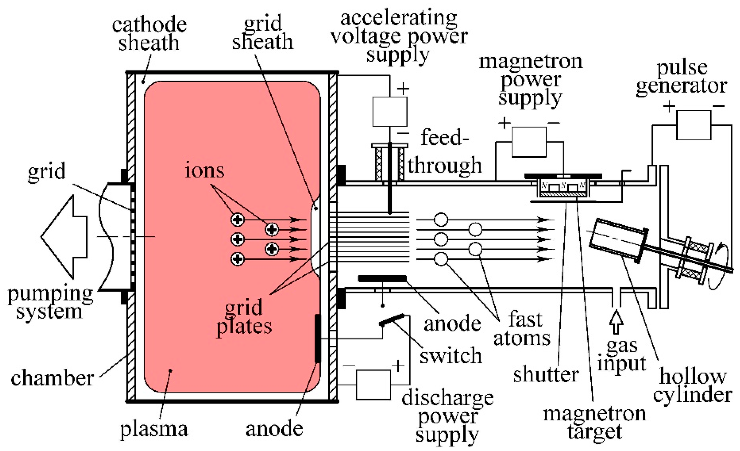
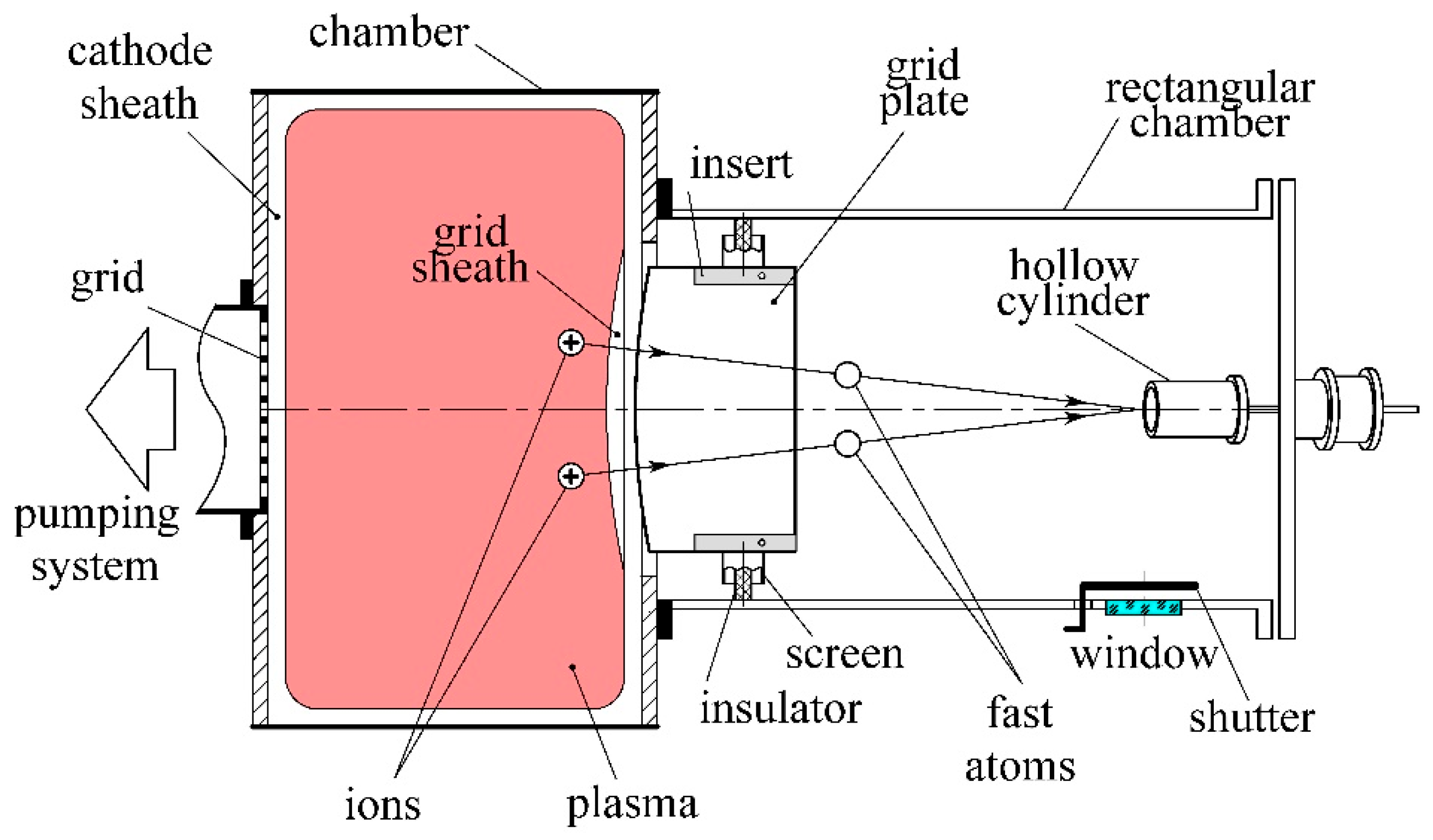
2.1. Experimental Setup
2.2. Filling the Chambers with Plasma
2.3. Instruments for Characterisation of the Samples
- -
- cut-offs—0.025/0.08/0.25/0.8/2.5/8.0 (mm), selectable;
- -
- tracing speed Vt—0.05/0.15/0.5 mm/s, or variable 0.01–2.0 mm/s in 0.01 increments;
- -
- tracing length lt—0.48/1.5/4.8/15/48 mm or variable 0.1–200 mm;
- -
- measuring length lm—0.40/1.25/4.0/12.5/40 mm or variable;
- -
- cut-off λ (mm)—0.08/0.25/0.8/2.5/8.0;
- -
- Gauss—digital filter (mm) cut-offs 0.025/0.08/0.25/0.8/2.5/8.0.
- -
- Stylus tip radius 2 µm.
- -
- Software TURBO ROUGHNESS, Hommel Map Expert 4.1.
| Temperature measurement range: | 200–1300 °C |
| Spectral range: | 2–2.8 µm |
| IR detector: | PbS |
| Radiation coefficient (ε): | 0.1 … 1.0 |
| Reproducibility: | 0.1% of the measured value °C + 1 °C |
| Dimensions (L × W × H): | 195 mm × 56 mm × 62.5 mm |
| Dimensions of the slide table, mm | 150 × 150 |
| Maximum Z-axis clearance, mm | 140 |
| Load range, N | 1–40 |
| Minimum noise level, min | 0.75 |
| Depth range, µm | 300 |
| Depth detection accuracy, nm | 10 |
| Scratching speed, mm/min | 0–240 |
| Lens magnification | 10×, 20×, 50× and 100× |
| Thickness | Exceeding the depth of indentation at least 10 times |
| Surface | plane-parallel |
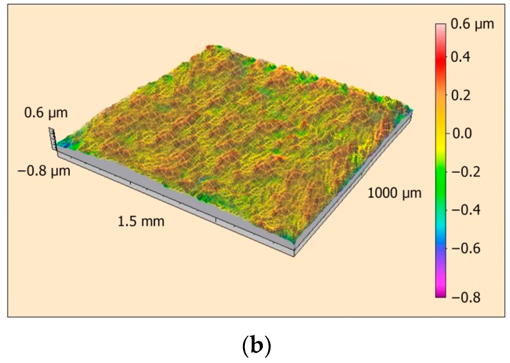
3. Results
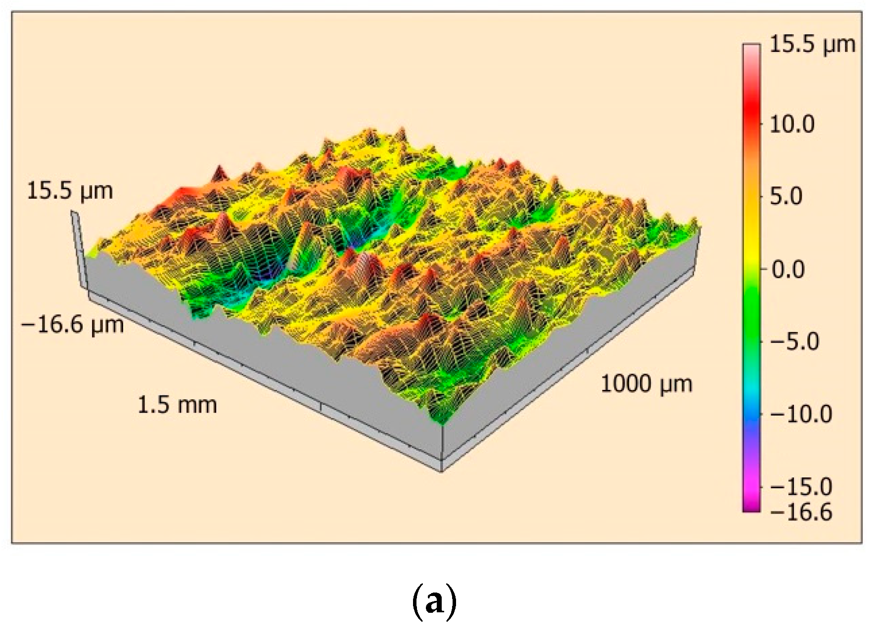
3.1. Explosive Ablation of Superficial Protrusion
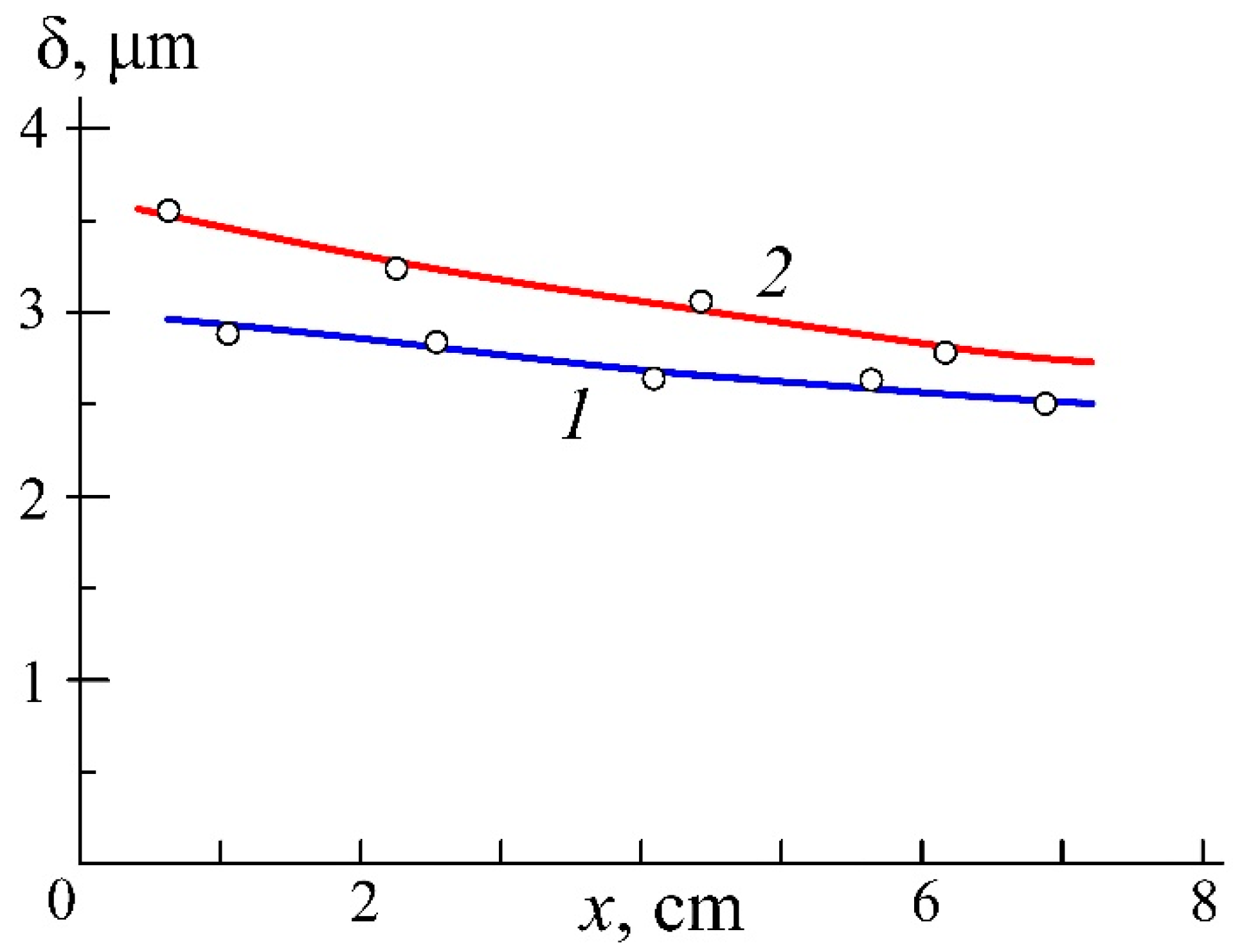
3.2. Polishing with a Beam of Fast Argon Atoms
3.3. Coating Deposition
4. Discussion
5. Conclusions
- 1.
- The study of polishing a part with a beam of fast argon atoms with a large angle of incidence on the part surface showed that, with the help of the beam, it is possible to significantly increase the surface finish class.
- 2.
- Deposition on a part of a coating with a thickness significantly exceeding the height of the protrusions on its surface does not reduce its roughness.
- 3.
- A simultaneous deposition of coating on a part surface being sputtered by a beam of fast argon atoms with a large angle of incidence to the surface noticeably increases the polishing speed.
- 4.
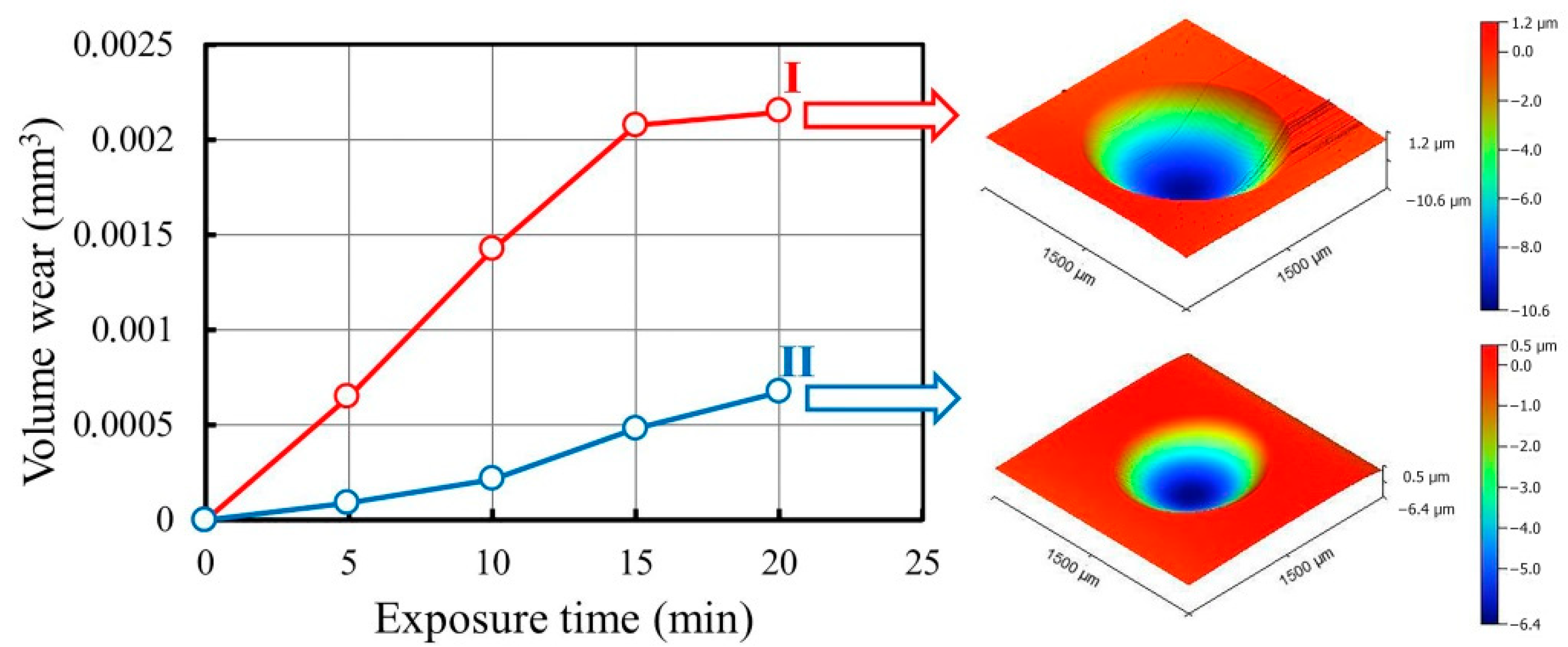
- Due to combined treatment of the part with explosive ablation of surface protrusions, polishing with a beam of fast neutral atoms, and deposition of wear-resistant coating, the coating adhesion was substantially improved and the abrasive wear became three times smaller.
Author Contributions
Funding
Institutional Review Board Statement
Informed Consent Statement
Data Availability Statement
Acknowledgments
Conflicts of Interest
Abbreviations
| d | Diameter of the notch, mm |
| I | Discharge current, A |
| L | Length of electrons path from the chamber wall to the anode, m |
| l | Evaluation width, mm |
| lt | Tracing length, mm |
| ln | Evaluation length, mm |
| lr | Sampling length, mm |
| p | Gas pressure in the chamber, Pa |
| po | Critical pressure, Pa |
| Ra | Arithmetical mean deviation of the roughness profile, μm |
| rtip | Stylus tip radius, μm |
| Sa | Anode surface area, m2 |
| U | Grid plates voltage, V |
| Ua | Accelerating voltage, V |
| Ud | Discharge voltage, V |
| V | Chamber volume, m3 |
| vt | Tracing speed, mm/s |
| W | Gas ionization cost, eV |
| α | Angle of incidence of fast atoms on the treated surface, ° |
| Λ | Path, during the passage of which the electrons emitted by the chamber spend all their energy, m |
| λc | Long-wave profile filter, mm |
References
- Danilov, I.; Hackert-Oschätzchen, M.; Zinecker, M.; Meichsner, G.; Edelmann, J.; Schubert, A. Process Understanding of Plasma Electrolytic Polishing through Multiphysics Simulation and Inline Metrology. Micromachines 2019, 10, 214. [Google Scholar] [CrossRef] [PubMed]
- Chirkov, A.M.; Rybalko, A.P.; Rogalsky, Y.I.; Sedoy, E.A.; Merkuhin, A.V.; Borisov, N.V. The Method of Laser-Plasma Polishing of a Metallic Surface. RF. Patent RU 2381094, 10 February 2010. [Google Scholar]
- Obeidi, M.A.; McCarthy, E.; O’Connell, B.; Ahad, I.U.; Brabazon, D. Laser Polishing of Additive Manufactured 316L Stainless Steel Synthesized by Selective Laser Melting. Materials 2019, 12, 991. [Google Scholar] [CrossRef] [PubMed]
- Koval, N.N.; Teresov, A.D.; Ivanov, Y.F.; Petrikova, E.A. Pulse Electron-Beam Metal Product Surface Polishing Method. RF. Patent RU 2619543, 16 May 2017. [Google Scholar]
- Abdul-Kader, A. Surface modifications of PADC polymeric material by ion beam bombardment for high technology applications. Radiat. Meas. 2014, 69, 1–6. [Google Scholar] [CrossRef]
- Škereň, T.; Veselý, M.; Čapek, P.; Král, J. Ion-induced nanopattern propagation on metallic surfaces. Phys. Rev. B 2015, 92, 235406. [Google Scholar] [CrossRef]
- Ieshkin, A.E.; Kushkina, K.D.; Kireev, D.S.; Ermakov, Y.A.; Chernysh, V.S. Polishing superhard material surfaces with gas-cluster ion beams. Tech. Phys. Lett. 2017, 43, 95–97. [Google Scholar] [CrossRef]
- Maishev, Y.P.; Shevchuk, S.L.; Kudrya, V.P. Generation of fast neutral beams based on closed drift ion sources. Russ. Microelectron. 2014, 43, 345–351. [Google Scholar] [CrossRef]
- Nam, S.K.; Economou, D.J.; Donnelly, V.M. Generation of Fast Neutral Beams by Ion Neutralization in High-Aspect-Ratio Holes: A Particle-in-Cell Simulation Study. IEEE Trans. Plasma Sci. 2007, 35, 1370–1378. [Google Scholar] [CrossRef]
- Metel, A.S.; Grigoriev, S.N.; Melnik, Y.A.; Bolbukov, V.P. Broad beam sources of fast molecules with segmented cold cathodes and emissive grids. Instrum. Exp. Technol. 2012, 55, 122–130. [Google Scholar] [CrossRef]
- Gusarov, A.V.; Grigoriev, S.N.; Volosova, M.A.; Melnik, Y.A.; Laskin, A.; Kotoban, D.V.; Okunkova, A.A. On productivity of laser additive manufacturing. J. Mater. Process. Technol. 2018, 261, 213–232. [Google Scholar] [CrossRef]
- Smurov, I.; Doubenskaia, M.; Grigoriev, S.; Nazarov, A. Optical Monitoring in Laser Cladding of Ti6Al4V. J. Therm. Spray Technol. 2012, 21, 1357–1362. [Google Scholar] [CrossRef]
- Kelly, P.J.; Arnell, R.D. Magnetron sputtering: A review of recent developments and applications. Vacuum 2000, 56, 159–172. [Google Scholar] [CrossRef]
- Anders, A. Tutorial: Reactive high power impulse magnetron sputtering. J. Appl. Phys. 2017, 121, 171101. [Google Scholar] [CrossRef]
- McDaniel, E.W. Collision Phenomena in Ionized Gases; Willey: New York, NY, USA, 1964. [Google Scholar]
- Phelps, A.V. Cross Sections and Swarm Coefficients for Nitrogen Ions and Neutrals in N2 and Argon Ions and Neutrals in Ar for Energies from 0.1 eV to 10 keV. J. Phys. Chem. Ref. Data 1991, 20, 557–573. [Google Scholar] [CrossRef]
- Phelps, A.V.; Greene, C.H.; Burke, J.P. Collision cross sections for argon atoms with argon atoms for energies from 0.01 eV to 10 keV. J. Phys. B At. Mol. Opt. Phys. 2000, 33, 2965–2981. [Google Scholar] [CrossRef]
- Metel, A.S.; Grigoriev, S.N.; Melnik, Y.; Panin, V.V. Filling the vacuum chamber of a technological system with homogeneous plasma using a stationary glow discharge. Plasma Phys. Rep. 2009, 35, 1058–1067. [Google Scholar] [CrossRef]
- Metel, A.S.; Bolbukov, V.P.; Volosova, M.A.; Grigoriev, S.N.; Melnik, Y.A. Equipment for deposition of thin metallic films bombarded by fast argon atoms. Instrum. Exp. Techol. 2014, 57, 345–351. [Google Scholar] [CrossRef]
- Dalgarno, A. Range and Energy loss. In Atomic and Molecular Processes; Bates, D.R., Ed.; Academic Press: New York, NY, USA, 1962; Volume 13, pp. 622–642. [Google Scholar]
- Langmuir, I. The interaction of electron and positive ion space charges in cathode sheaths. Phys. Rev. 1929, 33, 954–989. [Google Scholar] [CrossRef]
- Anders, A. Cathodic Arcs: From Fractal Spots to Energetic Condensation; Springer: New York, NY, USA, 2008. [Google Scholar]
- Sobol, O.; Andreev, A.; Grigoriev, S.N.; Volosova, M.A.; Gorban’, V.F. Vacuum-arc multilayer nanostructured TiN/Ti coatings: Structure, stress state, properties. Met. Sci. Heat Treat. 2012, 54, 28–33. [Google Scholar] [CrossRef]
- Behrisch, R. Physical Sputtering of Single-Element Solids. In Sputtering by Particle Bombardment; Behrisch, R., Ed.; Springer: New York, NY, USA, 1981. [Google Scholar]
- Kaminsky, M. Atomic and Ionic Impact Phenomena on Metal Surfaces; Springer: Berlin/Heidelberg, Germany, 1965. [Google Scholar]
- Moll, E.; Bergmann, E. Hard coatings by plasma-assisted PVD technologies: Industrial practice. Surf. Coat. Technol. 1989, 37, 483–509. [Google Scholar] [CrossRef]
- Ruset, C.; Grigore, E. The influence of ion implantation on the properties of titanium nitride layer deposited by magnetron sputtering. Surf. Coat. Technol. 2002, 156, 159–161. [Google Scholar] [CrossRef]
- Grigore, E.; Ruset, C.; Short, K.; Hoeft, D.; Dong, H.; Li, X.; Bell, T. In situ investigation of the internal stress within the nc-Ti2N/nc-TiN nanocomposite coatings produced by a combined magnetron sputtering and ion implantation method. Surf. Coat. Technol. 2005, 200, 744–747. [Google Scholar] [CrossRef]


| Type of Profilometer | Hommel Tester T8000 (Hommelwerke GmbH, Germany) |
|---|---|
| Stylus type | TKU 300 |
| Tracing length | lt = 2.0 mm |
| Evaluation length | ln = 1.5 mm |
| Sampling length | lr = 0.25 mm |
| Evaluation width (3D measurements) | l = 1.0 mm |
| Number of stylus passes (3D measurements) | 201 |
| Distance between stylus tracks (3D measurements) | 5 μm |
| Stylus tip radius | rtip = 2 μm |
| Stylus tip angle | 90° |
| Tracing speed | vt = 0.05 mm/s |
| Long-wave profile filter (cutoff) | λc = 0.25 mm |
| Measuring range | ±80 μm |
| Gaussian digital filter | 80 μm |
| Software | TURBO ROUGHNESS, Hommel Map Expert 4.1. |
Publisher’s Note: MDPI stays neutral with regard to jurisdictional claims in published maps and institutional affiliations. |
© 2022 by the authors. Licensee MDPI, Basel, Switzerland. This article is an open access article distributed under the terms and conditions of the Creative Commons Attribution (CC BY) license (https://creativecommons.org/licenses/by/4.0/).
Share and Cite
Grigoriev, S.; Metel, A.; Volosova, M.; Melnik, Y.; Mustafaev, E. Combined Treatment of Parts Produced by Additive Manufacturing Methods for Improving the Surface Quality. Technologies 2022, 10, 130. https://doi.org/10.3390/technologies10060130
Grigoriev S, Metel A, Volosova M, Melnik Y, Mustafaev E. Combined Treatment of Parts Produced by Additive Manufacturing Methods for Improving the Surface Quality. Technologies. 2022; 10(6):130. https://doi.org/10.3390/technologies10060130
Chicago/Turabian StyleGrigoriev, Sergey, Alexander Metel, Marina Volosova, Yury Melnik, and Enver Mustafaev. 2022. "Combined Treatment of Parts Produced by Additive Manufacturing Methods for Improving the Surface Quality" Technologies 10, no. 6: 130. https://doi.org/10.3390/technologies10060130
APA StyleGrigoriev, S., Metel, A., Volosova, M., Melnik, Y., & Mustafaev, E. (2022). Combined Treatment of Parts Produced by Additive Manufacturing Methods for Improving the Surface Quality. Technologies, 10(6), 130. https://doi.org/10.3390/technologies10060130