Article

Analysis of the Impact of Electrical and Timing Masking on Soft Error Rate Estimation in VLSI Circuits †

1
Department of Electrical and Computer Engineering, University of Thessaly, 38334 Volos, Greece
2
Department of Computer Science, University of Thessaly, 35131 Lamia, Greece
*
Authors to whom correspondence should be addressed.
This paper is an extended version of our paper published in Proceedings of the 34th IEEE International Symposium on Defect and Fault Tolerance in VLSI and Nanotechnology Systems (DFT), Athens, Greece, 6–8 October 2021.
These authors contributed equally to this work.
Technologies 2022, 10(1), 23; https://doi.org/10.3390/technologies10010023
Submission received: 29 December 2021 / Revised: 21 January 2022 / Accepted: 28 January 2022 / Published: 31 January 2022
(This article belongs to the Special Issue MOCAST 2021)

Abstract

:
Due to continuous CMOS technology downscaling, Integrated Circuits (ICs) have become more susceptible to radiation-induced hazards such as soft errors. Thus, to design radiation-hardened and reliable ICs, the Soft Error Rate (SER) estimation constitutes an essential procedure. An accurate SER evaluation is provided based on a SPICE-oriented electrical masking analysis, combined with a TCAD characterization process. Furthermore, the proposed work analyzes the effect of a Static Timing Analysis (STA) methodology and the actual interconnection delay on SER evaluation. An analysis of the generated Single Event Multiple Transients (SEMTs) and the circuit operating frequency that are related to the SER estimation is also discussed. Various benchmarks, synthesized utilizing a 45 nm and 15 nm technology, are employed, and the experimental results demonstrate the SER variation as the device node scales down.

1. Introduction

Over the past decades, the CMOS technology downscaling trend, which involves—among other factors—the shrinking of transistor dimensions, the reduction of supply voltages, and the increase in operating frequencies, has rendered modern Integrated Circuits (ICs) substantially susceptible to radiation-induced Single Event Transients (SETs) [1]. Thus, ICs’ reliability regarding Soft Errors constitutes a challenging field of research, especially when it concerns critical systems. A radiation particle of sufficient energy that strikes on a gate may generate, under certain circumstances, a glitch at the output. At the circuit level, a soft error emerges when a SET is captured by at least one storage element. While the soft errors are not permanent, they could potentially pose a severe threat to vulnerable modern chips, especially critical ones. A factor that aggravates this problem is the emergence of Single Event Multiple Transients (SEMTs) that, primarily due to the increase in the circuit device density, as a consequence of the Moore’s law, have become more prevalent recently [2]. In light of the above, the accurate evaluation of the Soft Error Rate (SER) constitutes a vital process to determine the ICs susceptibility to radiation hazards. Usually, the SER is measured in terms of FIT (Failures In Time), which is a widely-used reliable metric across different SER estimation tools for the assessment of chips’ reliability.
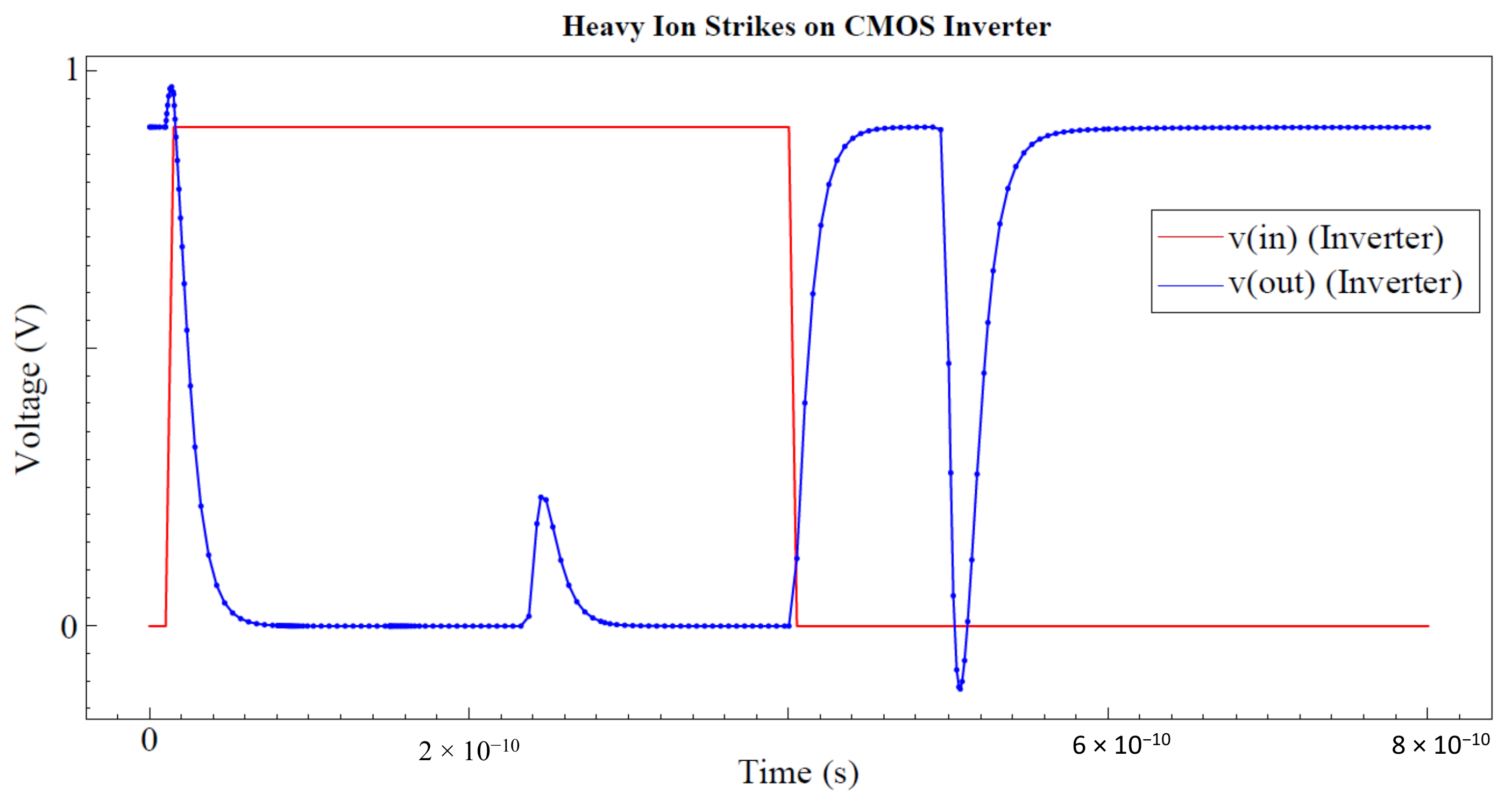
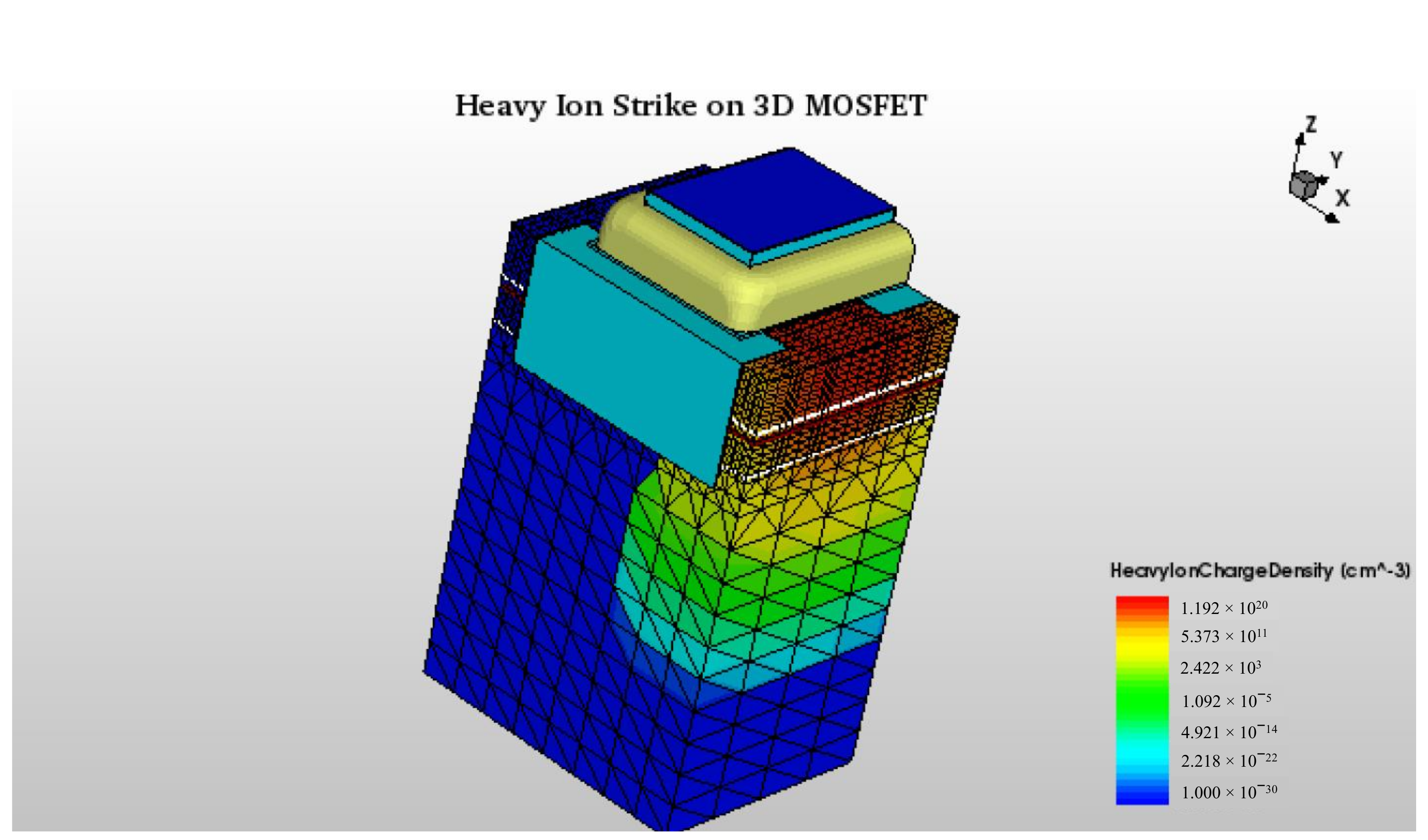
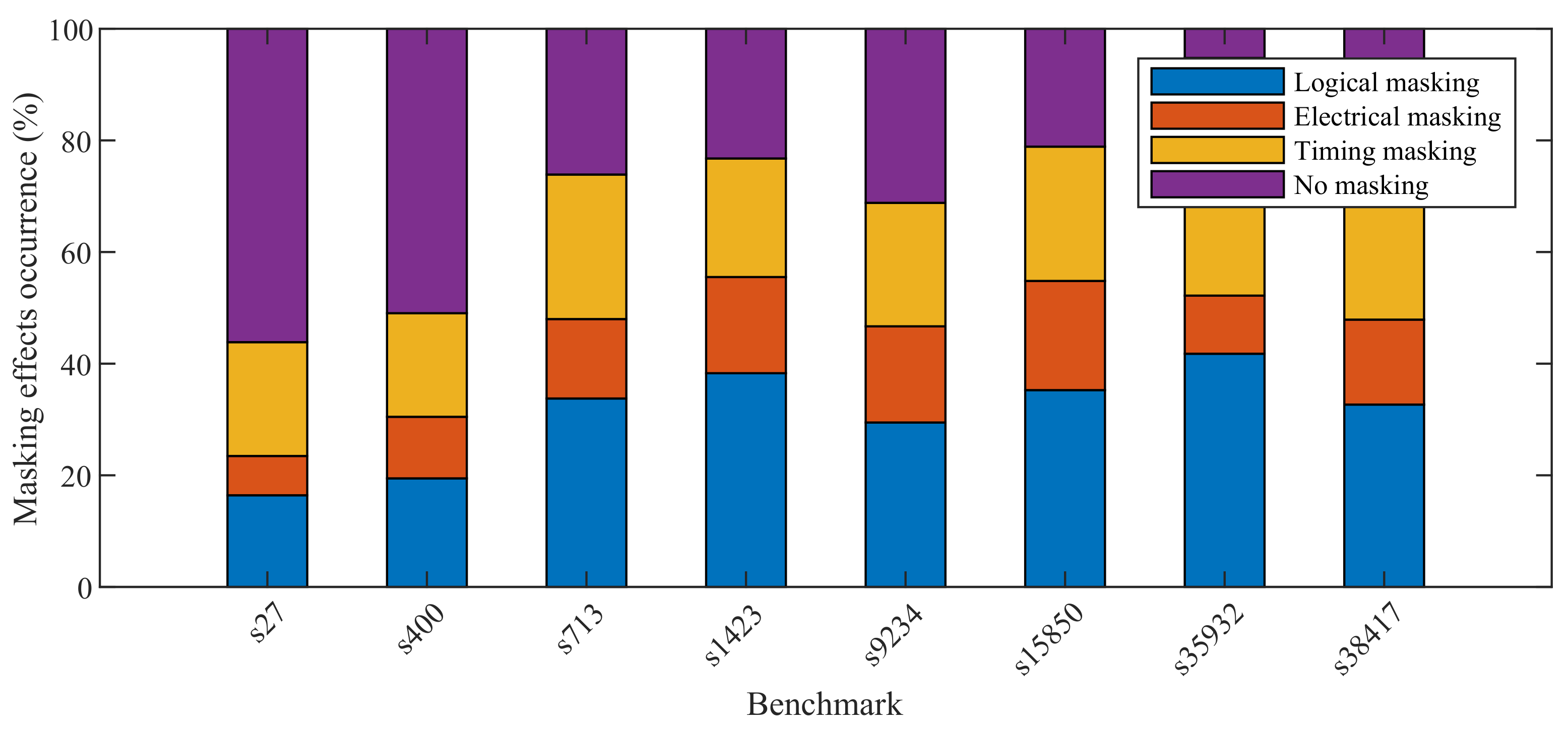
To accurately estimate the SER of a design, it is indispensable to model sufficiently and accurately the three mechanisms that are able to impede an SET from propagating through a circuit and, eventually, being latched by the flip-flops (FFs), thus producing a soft error. These effects are logical, electrical, and timing-masking [
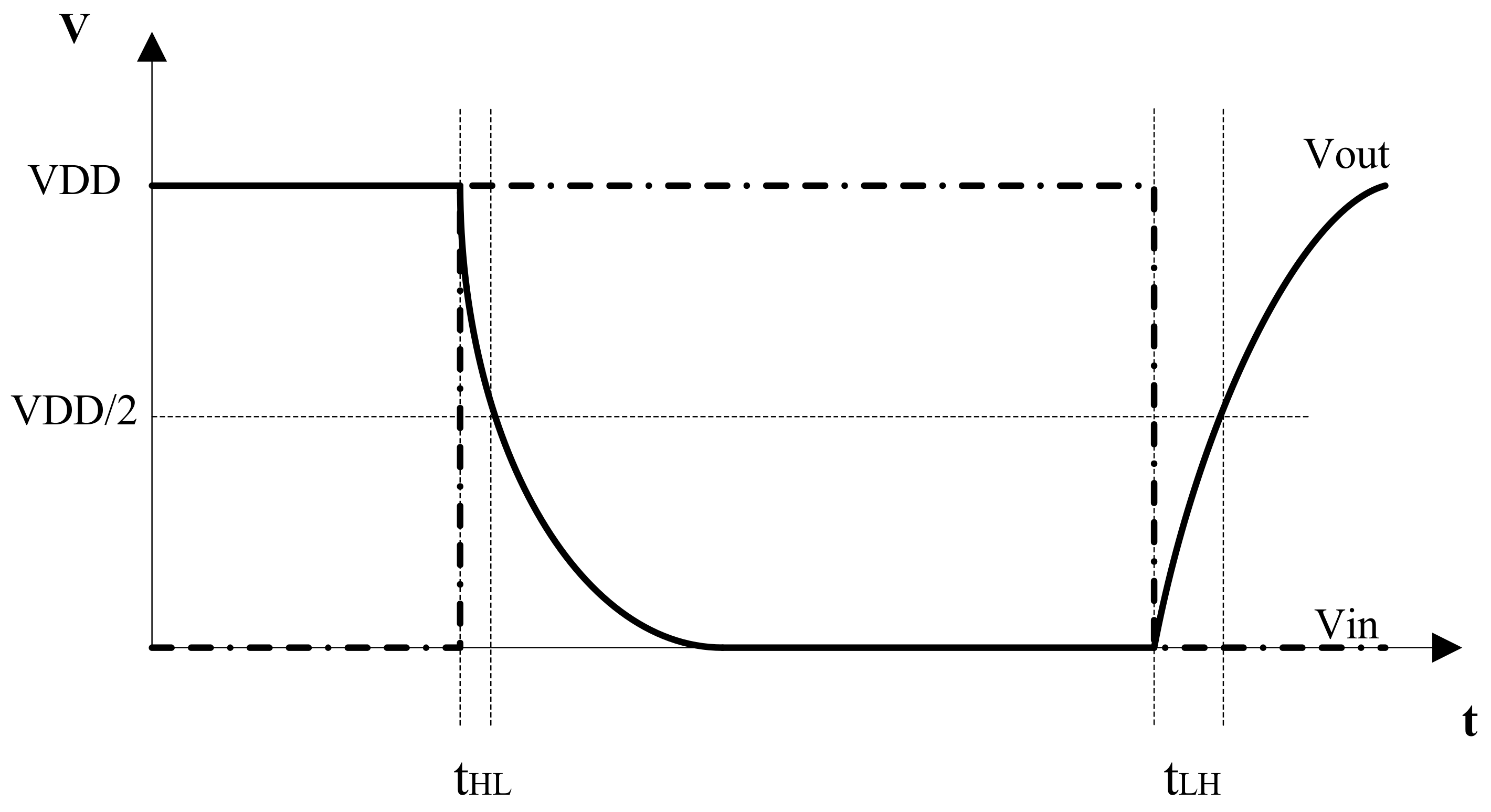
3]. The logical masking occurs when an SET is masked on a subsequent gate because one of the other inputs is in a controlling value. For example, the controlling value of an AND gate is logic 0, whereas logic 1 is the controlling value of an OR gate. The electrical masking is associated with the electrical properties of the gates and the SET pulse characteristics and occurs as the SET pulse attenuates during the propagation through the logic gates, becoming too small to be reliably latched at the FFs. Finally, the timing-masking occurs when an SET arrives outside the latching window of the FF as this is determined by setup and hold times.
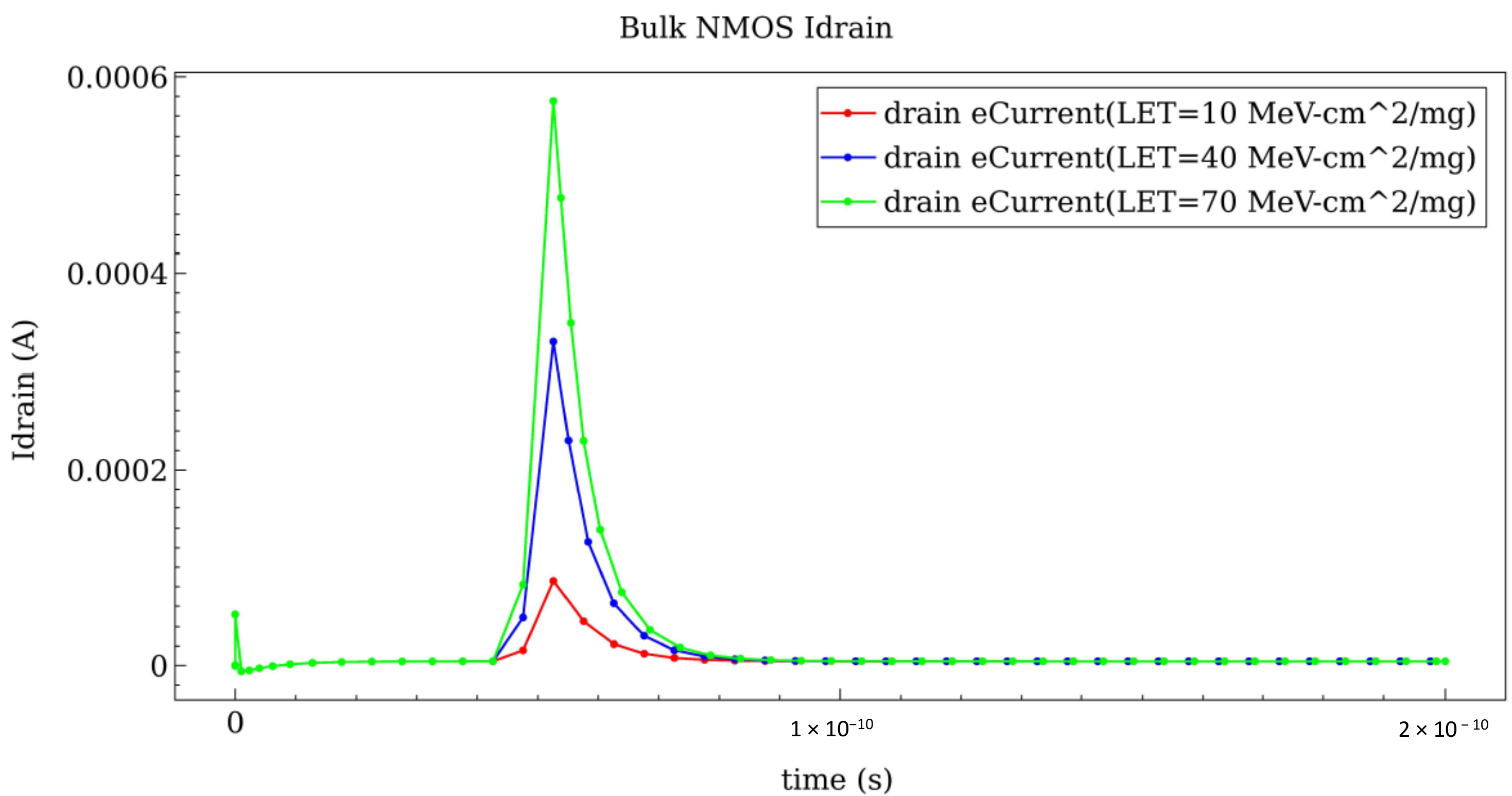
The modeling of the three masking mechanisms is equally significant in obtaining an accurate estimation of a circuit’s vulnerability to radiation hazards. The logical masking is quite straightforward to model, and there are no major differences among the various SER estimation works, with the more prevalent model being the utilization of a simple logic level simulator. However, the electrical and timing-maskings can be modeled in many different ways, which determine the overall accuracy of the SER estimation. Plenty of work that attempts to model accurately the electrical masking mechanism has been proposed so far. Generally, there are two types of approaches that dominate the bibliography. The first is based on SPICE simulations to accurately characterize the propagated SET pulses and form LookUp Tables (LUTs), whereas the other attempts to estimate the effect of electrical masking through analytical modeling. The advantage of the former is its accuracy, even though it is expensive in terms of time, whereas the latter is more efficient but lacks accuracy. A closed-form approximation of the logic level waveforms, induced by α-particles on inverters considering the transistor’s pull-up and pull-down network, the particle charge, and the capacitive loads, is presented in [4]. In [5], a closed-form expression is introduced to calculate the output voltage (amplitude) of a propagated transient fault. However, in [6] a simple ramp approximation equation is used to estimate the SET pulse width at the gate output. An approach that utilizes discrete values of the input waveform to approximate the whole output pulse (amplitude and duration) is presented in [7]. In [8], a pre-characterization library process, based on the SET pulse height and width at the gate input, is carrried out to extract parameters and form simple analytical continuous functions for pulse propagation. In [9], a two-phase pre-characterization process is performed with SPICE, forming LUTs utilized in the extraction of SET propagation mathematical equations. In [10,11], SPICE simulations are performed to characterize the SET width. Other approaches use transistor models to effectively model the electrical masking effect [12,13]. Recent works have revealed another significant aspect of SET propagation that affects its pulse width. In particular, the investigation of the SETs production and propagation in CMOS logic circuits, in [
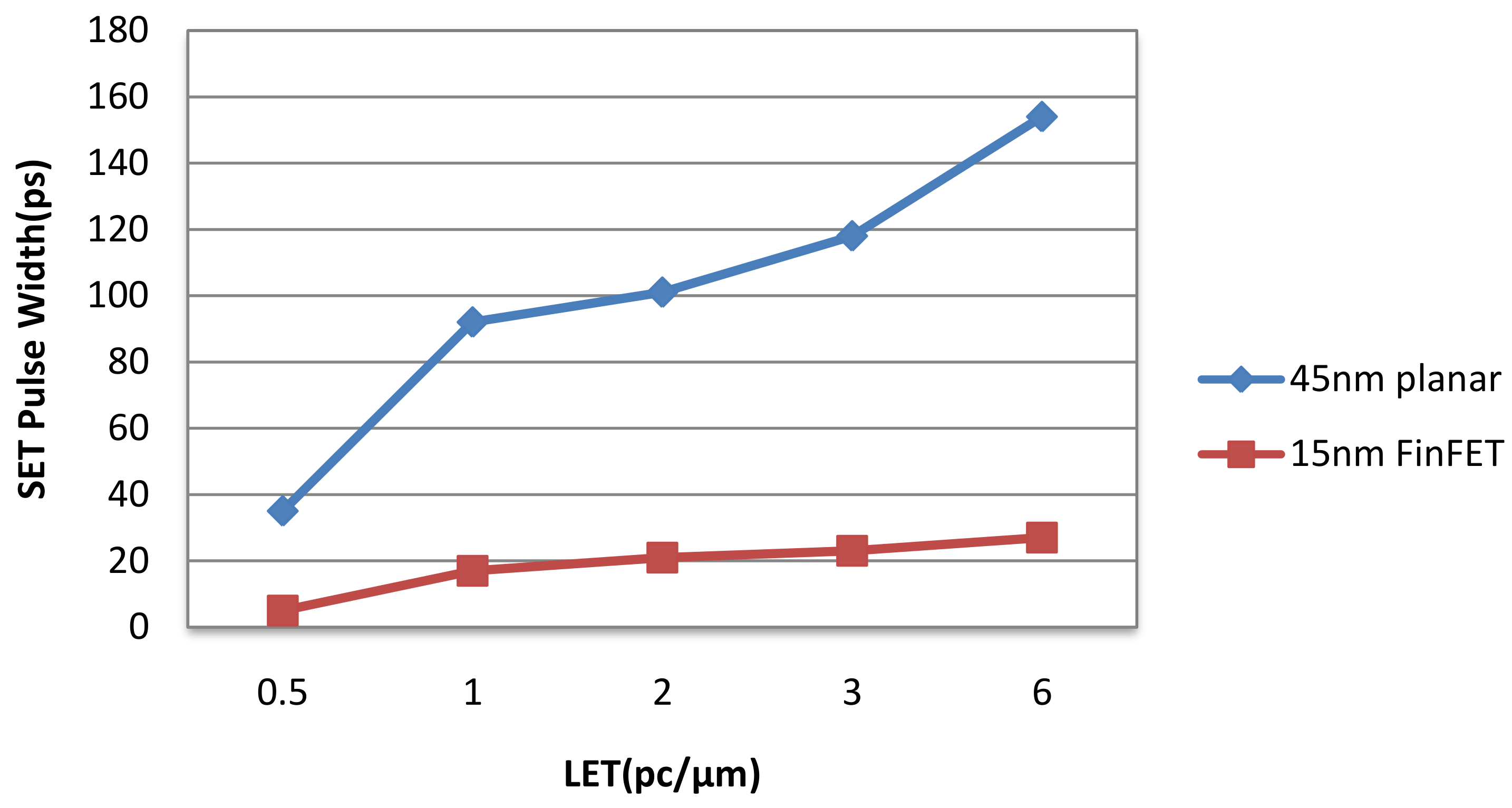
14], has shown that they may propagate without attenuation when they are generated from particle strikes of certain linear energy transfer. In [15], the authors present the Propagation-Induced Pulse-Broadening (PIPB) effect that a SET is subjected to as it propagates through long inverter chains. A direct relationship is reported between the SET pulse attenuation or broadening with the circuit design parameters and the gate delay [16,17]. The TCAD simulations of inverter chains in [18] relate the PIPB effect to the transistor voltage threshold. The impact of the propagation paths (including reconvergent paths), the input patterns, and the polarity of the SET on the PIPB effect is presented in [19]. The authors in [20] characterize the PIPB effect on SETs generated from a heavy ion microbeam and associate the transistor size with its confinement. All these works indicate that this aspect should be taken into account to achieve an accurate SER evaluation. A similar phenomenon of SET pulse broadening after narrowing (PBAN) due to the charge sharing is examined in [21]. As regards the timing-masking modeling, there is a lack of information in the bibliography upon the impact of each timing analysis approach on the SER estimation. A modified static timing analysis for the timing-masking modeling is proposed in [22], but the utilized delay model is not clarified, and the interconnection delay is ignored, which may underestimate or overestimate the results.
This work aims at placing an emphasis on the significance of the electrical and timing-masking model that is utilized from a SER estimation tool to achieve an efficient and accurate evaluation of modern ICs’ vulnerability to radiation hazards. The applied timing analysis holds a key role in the modeling of both electrical and timing-masking mechanisms. Based on the results of the STA analysis, with respect to the fall/rise delays and the SPICE simulations, we are able to determine the SET pulse width as it propagates through the logic gates. Since the output pulse width depends on the input of the SET, which implies different fall and rise delays, the modeling of electrical masking becomes dynamic. As regards the timing-masking, the STA analysis that we implement ensures that the delay of the SET is calculated accurately as it propagates until FFs. The impact of interconnection wiring on SET pulse propagation delay is also discussed. The results of the electrical and timing-masking are validated with SPICE, indicating fairly good accuracy. Some preliminary results of this paper were presented in [23].
The rest of this work is organized as follows. 
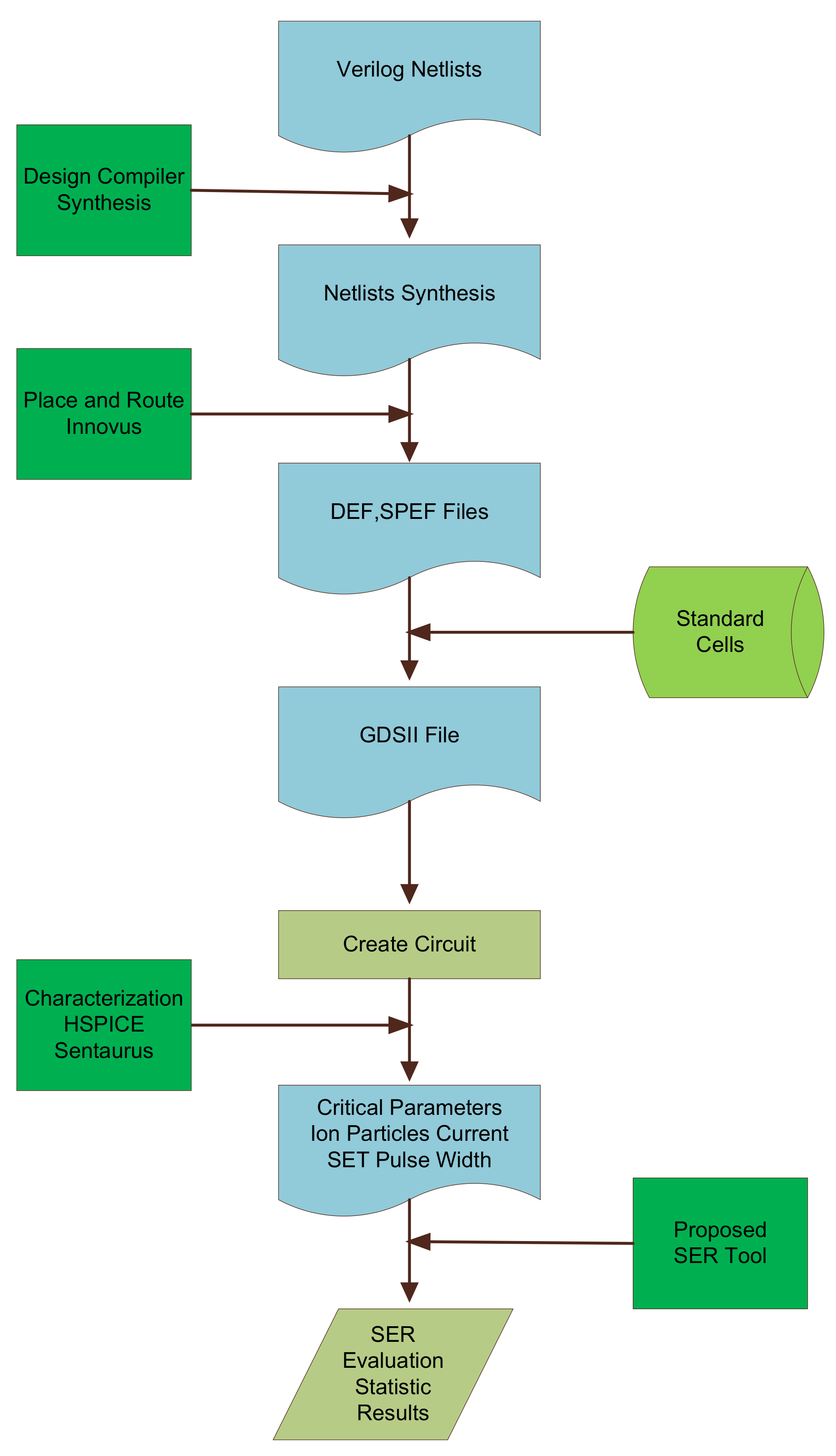
Section 2 presents a TCAD simulation-based approach to achieve an accurate characterization of the radiation-induced SET pulses. Section 3 elaborates on the analysis and modeling of electrical masking and discusses the relationship of this model with the timing analysis approach selected for the SER estimation. Section 4 briefly highlights the main steps of the integrated SER evaluation flow that the aforementioned masking models are incorporated into. Section 5 verifies the electrical and timing-masking models and presents a series of experimental results on a variety of benchmarks regarding the impact of these models on SER estimation. Finally, Section 6 concludes this work.

2. Radiation-Aware TCAD Simulations

Radiation-induced soft errors constitute a reliability issue that is related to physics phenomena, which supersede the particle strike event, and which involve the interaction between the high-energy particle that strikes the silicon and the particles of the device. A certain approach to model such phenomena is real-time experiments through neutron beam setups and actual measurements of DUTs. However, they are time consuming and thus inefficient to model and characterize the electrical behavior of the devices across a wide spectrum of technology nodes. Therefore, TCAD tools are extremely useful in modeling, simulating, and optimizing the semiconductor process technologies and devices since they provide solutions that are based on deep physical equations.
One of the features of TCAD tools is that they provide an effective method to model and simulate the impact of SETs on semiconductor devices through their integrated physics background. In this work, various TCAD simulations are performed to identify the pulse of the generated SET. In particular, several simulations of particles striking the drain of NMOS and PMOS transistors model the induced disturbance. Figure 1 shows the charge generation as a heavy ion strikes the drain of an NMOS transistor with 90° angle, which is vertical to the drain contact, and its distribution within the transistor’s mesh. Additionally, note that the width and the length of the NMOS drain are W = 25 nm and L d = 10 nm, respectively.
The energy of the radiation particle corresponds to the Linear Energy Transfer (LET) that delivers as it penetrates the semiconductor and is a crucial factor in such type of simulations. The resultant charge generation as a heavy ion strikes the drain is reflected in the drain current. Figure 2 presents the drain current for three different LETs of the heavy ion. This graph shows that the current spike elevates as the energy increases, indicating the significance of heavy ion severity in the generation of SETs and, subsequently, in the emergence of soft errors.
A radiation-aware simulation of an NMOS or PMOS device might be sufficient to model the impact of such hazards on semiconductor devices, but at a logical level, there is an additional step that should to be considered. That is, we need to examine if the charge generation within the device emerges at the output of the corresponding logic gate and, if so, identify the shape (i.e., height, width, and slew) of the SET pulse. Thus, a mixed-mode simulation that combines the semiconductor devices based on physical models (TCAD) with devices described with compact models (SPICE) can be performed to observe the generated SET. In this way, the simulation of a heavy ion striking a node becomes more accurate as we are able to incorporate into the simulation the physical devices (i.e., transistors) that are modeled with a powerful TCAD tool. Figure 3 demonstrates a transient analysis of an inverter, performed with mixed-mode simulation, when two heavy ions strike the gate at different time moments. Note that the time moments are quite close, considering such a small time frame, which a rather unlikely scenario for two radiation particles striking the same cell within a few picoseconds. Therefore, this simulation setup is deliberately presented in this mode, to exhibit in the same graph the effect of SET pulse generation at the output of a logic cell in two cases. The first considers a particle striking the off PMOS transistor device and the second a particle striking the off NMOS, generating at the output a small and a large glitch, respectively. The difference in the SET amplitudes is attributed to the higher sensitivity of NMOS transistor compared to PMOS.

3. Electrical and Timing-Masking Model

The most significant factor in the estimation of SER in the combinational logic of ICs is the modeling of the three masking effects. Since the masking mechanisms are contingent on the connectivity and the design properties of the individual circuits, their impact varies from one circuit to another. Figure 4 presents the distribution of the generated SETs in an SER estimation process with respect to the type of masking (i.e., logical, electrical, and timing) that occurs or not when the same number of faults are injected. While logical masking appears to be the most prevalent factor contributing to the SET elimination, especially for the large-scale benchmarks, electrical and timing-masking jointly tend to be similarly substantial, if not more. This graph reveals the necessity of a sufficient and accurate modeling of masking mechanisms since this reflects on the SER estimation eventually.

3.1. Electrical Masking

The propagation of SETs is affected, to a great extent, by electrical masking, which is a critical factor that should be modeled sufficiently. In the context of this work, a comprehensive modeling of electrical masking that contributes to the SER evaluation accuracy is provided. SPICE simulations constitute a widely-utilized practice to model the SET pulse generation. In order to analyze gate susceptibility at the transistor level, current pulses are connected on the transistor nodes to generate SETs at the gate output. Therefore, to model the disturbance induced by the particle strike, which results in a 1→0 or 0→1 momentarily transition, current pulses are injected into PMOS and NMOS transistors. Generally, it should be highlighted that the modeling of the SET pulse is a crucial procedure since it may propagate through the circuit and be latched by a storage element if it is of sufficient duration and amplitude.
Figure 5 shows a SET pulse, which passes through a CMOS logic gate (e.g., an inverter) and is modeled as a trapezoidal waveform. The transition from logic 1 (high voltage) to logic 0 (low voltage) and from logic 0 to logic 1 constitutes the individual propagation delays for the rise and fall transitions of the output pulse, respectively, and is employed to determine the pulse propagation delay. More specifically, the high-to-low propagation delay t H L is the time interval from the point that input reaches 50% of the voltage supply (VDD) (i.e., logic 0 to logic 1 transition) to the point that output reaches 50% of VDD (i.e., logic 1 to logic 0 transition). The low-to-high propagation delay t L H is determined similarly.
Through an adequate number of SPICE simulations, it is observed that the transient pulse is deformed as it propagates through a logic gate, thus allowing for the modeling of the SET pulse propagation through a logic path. SET pulses of various output capacitance loads and several widths are taken into consideration. It should be emphasized that the applied output capacitance corresponds to the number of fanouts that a gate may have as well as the interconnection parasitics at its output, which means that it is a significant parameter for the delay of the pulse.
Table 1 presents the results of the SPICE simulations on the NAND2 and NOR2 gates when a SET pulse emerges on one input, whereas the other input is at a non-controlling value, so as the pulse is not logically masked, resulting in a 0→1→0 transition. The t L H and t H L as well as the output pulse width are measured for the different values of the output capacitance, indicating that they are directly related. It is clearly noticeable that the output pulse width results from the propagation delays t L H and t H L and, particularly, their difference. Therefore, for NAND2 gate the output pulse is calculated using Equation (1), whereas for NOR2 gate the output pulse is obtained from Equation (2).
Similarly, Table 2 presents the respective pulse characteristics for the opposite transition, i.e., 1→0→1. However, compared to the previous case, the pulse width of NAND2 gate is calculated with Equation (2).
V o = V i n + ( t L H t H L )
V o = V i n + ( t H L t L H )
The main observation from the SPICE results is that when a pulse propagates through a gate, its width may broaden or attenuate, depending on the transition and the gate type. Furthermore, note that for the 0→1→0 transition, as presented in Table 1, and for high capacitance values, the output pulses are equal to zero when SET width is 100 ps. This is due to the fact that the amplitude of the particular output pulses does not exceed the transition threshold (i.e., VDD/2), which means that it is not sufficient to propagate to the next stage and settle to a faulty voltage level. Additionally, it is worth to mention that there is a slight divergence between the measured output pulse and the actual difference between t H L and t L H delays, which results from the SPICE simulations and the parameters of the transistor models utilized.
Generally, there are difficulties in the practice of creating LUTs from SPICE simulations to model electrical masking, even though it is considered accurate. In particular, it is unfeasible to consider and analyze all the possible SET pulses that may emerge in a circuit since their shape characteristics change continuously when propagating through numerous circuit paths. Besides, complex LUTs may arise from the number of different factors that should be considered, such as the slews of the SET pulse, the parasitic capacitance, and the type of gates, thereby increasing the calculation cost and the memory usage. At the same time, this characterization procedure needs to be conducted for each utilized CMOS technology. These severe shortcomings are bypassed in this work by implementing an enhanced timing analysis methodology. Based on the deduction that the pulse propagation is directly related to the propagation delays t L H and t H L , the output pulse width is calculated considering the transition of the pulse and utilizing the corresponding equation. The propagation delays are computed once, during the basic STA, rendering the electrical masking accurate and fast, compared to the expensive LUT-based approaches.

3.2. Timing Masking

The accurate analysis of timing-masking is vital in the SER estimation of a circuit since the timing properties of the SET when arriving at the FF input and the timing circuit parameters affect the emergence of a soft error. Therefore, for the circuit timing behavior investigation, i.e., the determination of both the gates delay and the critical path, utilizing a basic STA methodology is significant. In particular, the STA method is based on LUTs, which store the input transition rates and load capacitances for each logic cell. The LUTs are obtained from the properly defined Non-Linear Delay Model (NLDM) of CMOS libraries and are formed under typical, worst, fast, and slow case conditions. Thus, accurate modeling of the timing-masking can be achieved when this is based on an accurate STA methodology.
At the early stages of SER evaluation and disregarding gate logic values, the circuit critical path estimation is conducted by implementing the STA method. In this analysis, based on the timing sense of gate input pins, the propagation delay of the gate is calculated by taking into consideration the maximum delay of the individual input arcs. At the later stages of electrical and timing-masking, this analysis can be enhanced though. In particular, the SET propagation delay when passing through a gate, which is needed for the timing-masking modeling, is obtained by observing its transition and the input that emerges. Finally, we achieve a result that approximates the SPICE simulation results, by taking into account the actual propagation delay for the particular input instead of the maximum delay among all the inputs. As a result, in the context of timing-masking modeling, the enhanced STA is converted, in a sense, into a Dynamic Timing Analysis (DTA). Additionally, note that this analysis is made only for forward logic cones, i.e., the logic paths that the SET propagates until the FF inputs.

3.3. Interconnection Delay

The performance of the modern CMOS ICs, in terms of operating frequency, power consumption, etc., is to some extent affected by the interconnect wiring among their logic components (e.g., cells, blocks, etc.). The wiring within a circuit introduces parasitic quantities of resistance (R), capacitance (C), and inductance (L) that, jointly with the logic gates, determine the propagation delay of the signals. There are various approximate techniques that model and estimate the interconnection delay, during the pre-layout phase, by taking into account the gate fanouts and estimating the total wire length for the entire circuit. However, the actual interconnection network of a design can be obtained only after the Placement and Routing (P&R) process with the extraction of the corresponding Standard Parasitic Exchange Format (SPEF) file. This file represents the parasitic wire data, which include parasitic resistance, capacitance, and their interconnection, and may be further used for simulation purposes such as delay calculation.
Figure 6 presents a typical example of an existing RC network of a net as extracted from the SPEF file of a design. That is a distributed net model and is depicted as an RC-tree with two branches, which is the number of fanouts. Given such an RC network, we can compute the interconnection delay by applying various models, such as the traditional Elmore’s delay model [24]. However, its calculation is not presented since it is out of the scope of this work.
In the context of SER estimation, it is important to take into consideration the impact of interconnection delay on the SET pulse propagation. As regards the incorporation of the interconnection network into the SER estimation tool, a SPEF file parser has been implemented to account for the parasitics of each net and, then, estimate their delay. Moreover, the pulse width at the output of a gate is transformed to a new one at the inputs of the fanout gates considering the current parameters, such as slew and total wire capacitance. Thus, detailed modeling of the interconnection network is accounted for to obtain even more accurate results regarding circuit’s susceptibility.

4. SER Evaluation Integrated Process

To evaluate the SER considering the proposed electrical and timing-masking models, the ISCAS ’89 benchmarks were synthesized with Synopsys® Design Compiler™, using the 45 nm and 15 nm Open-Cell libraries [25], and their layouts were extracted using Cadence® Innovus™EDA tool. Figure 7 describes the overall procedure of this work.
In the previous section, we mentioned that the interconnection delay is calculated utilizing the SPEF files, which is an input to this tool. Additionally, the identification of the gate transistors position and the sensitive regions of each gate on the die, along with the circuit creation, are accomplished through the parsing of the DEF and GDSII files, which are extracted during the P&R process for the corresponding benchmarks. A gate’s output may be changed only if its sensitive regions are affected by a particle strike. SPICE simulations for both NMOS and PMOS transistors for all input combinations are performed by injecting current pulses extracted from Synopsys® Sentaurus™TCAD tool for different LETs and observing the output pulse to identify gate sensitivity. This process shows that, according to current input values, sensitive regions are regarded as inactive transistors, that is, NMOS and/or PMOS diffusion.
An integrated tool based on Monte-Carlo simulations, modeling the three masking phenomena (logical, electrical, and timing) that affect the probability that a transient fault will become a soft error and emphasizing on SEMTs analysis, is utilized for the SER evaluation process [26]. An SEMT occurs when a heavy ion strikes a sensitive area over the chip, producing glitches on adjacent cells. To achieve a detailed evaluation of the circuit sites sensitivity to radiation, each circuit layout is divided into several grids. The execution time is reduced considerably by exploiting this idea and implementing a parallel SER estimation of the grids. Two other significant parameters are the handling of reconvergent pulses and the effect of temperature. The former is something that is taken into account since the transient faults following multiple paths and reconverging at a subsequent gate are not negligible, whereas the latter is also considered, indicating that SER becomes greater when the temperature increases since the SET widths become more intense [26]. Furthermore, the electrical and timing-masking models, as they are described in the manuscript, depend mainly on the technology library utilized (45 nm and 15 nm standard cell library). In particular, the critical factor is the timing model that we choose from the current library. So, even if it seems inconvenient to perform such simulations for different technologies, it is attainable since one of our tool’s inputs is the technology library files. Finally, in this work we focus mainly on radiation as the primary source of SETs since it is the usual cause of glitches. However, our method can be readily expanded to include other sources of soft errors by considering the relevant induced charges (for example, currents delivered at the circuit inputs via mechanisms such as latchup).

5. Experimental Results

In this section, we provide a verification framework for the electrical and timing-masking modeling and demonstrate various experimental results regarding some critical factors in SER estimation and the different electrical and timing approaches. All the experiments are performed on an Intel Core i7-4790 @3.60 GHz machine with a Linux-based OS and 16 GB of RAM, whereas some of the ISCAS ’89 benchmark designs are utilized to evaluate this work and demonstrate the results. Additionally, the SER is estimated both in terms of FIT and as a probability.

5.1. Electrical and Timing Verification

To verify both the electrical and timing-masking that are implemented from the SER estimation tool, we extract different logic paths with respect to the number and type of logic gates from various benchmark designs. Subsequently, SPICE simulations are performed to model the propagation of SETs. More specifically, each path, which is a circuit part, is imported to SPICE, and a SET pulse is applied on the input of the first gate to perform a simulation and obtain the pulse width and overall path delay at the output of the last gate. The first two paths are extracted from the s27 design and the others from s298 and s400 designs. Furthermore, note that the other gate inputs are in non-controlling value during the simulation to impede logical masking occurs. Besides, we use the SER estimation tool to simulate the selected paths, applying a SET of the same width with SPICE to observe the pulse shape at the end of the path. The checked paths, the length of each one, and the output SET pulse width and propagation delay for both SPICE and tool’s simulations are shown in Table 3. The accuracy of the proposed approach reaches about 96%, which is acceptable considering the difference in execution time, since SPICE simulation is considered time consuming. Finally, note that this comparison is sufficient for the verification of the SER methodology as well, since the electrical and timing-maskings are two of the most important factors in SER estimation.

5.2. Effect of SEMTs and Operating Frequency on SER Estimation

As discussed in Section 4, the overall circuit SER is obtained by modeling the three masking mechanisms during the transient fault propagation, at logic level. The area that SEMTs may occur is determined by the energy of the radiation particle strike, whereas the shape (i.e., length, width, and slope) of the generated glitches depends mainly on the load capacitance and the device characteristics of each gate, e.g., the channel length, the width of diffusions. A logic cell characterization of SET pulse widths was conducted with TCAD and mixed-mode simulations to facilitate an accurate SER estimation. The TCAD simulations considering a conventional 45 nm MOSFET planar technology and a 15 nm FinFET non-planar (3D) technology indicated that the latter is more resistant to heavy ions than the former.
In particular, Figure 8 presents the generated SET pulse widths of an inverter —for these technologies—when heavy ions of different LETs strike the cell. We observe that while the LET of the heavy ion increases, the SET pulse width increases as well for both process technologies. However, the widths for the 45 nm increase steeply and are much greater compared to those for the 15 nm, which shows that the FinFET technology is more resistant to ionizing radiation. Additionally, something that should be underlined is that this difference is primarily attributed to the gate transistor layout and not to the different technology nodes.
The downscaling of the node technology comes with higher operating frequencies. However, in an SER point of view when the frequency increases, the probability that an SET will be latched by a memory element increases as well. Table 4 presents the minimum clock period for some benchmarks as this was calculated during the timing analysis. The period of the benchmarks synthesized with respect to the 15 nm technology is significantly decreased compared to the period of the benchmarks at 45 nm technology. This means that it is more probable that an SET will not be masked, which is expected to reflect on the SER.
Another critical aspect of SER estimation that is affected from the downscaling of the device node is the number of the SEMTs that may appear in a simulation. An analysis of the circuit sites that are affected from the injection of radiation particles on different locations of the circuit layout is presented in the following tables. In particular, Table 5 presents the total number of particles injected, the number of SEMTs that these particles created, the overall number of affected gates from the corresponding SEMTs, and (finally) the percentage of the hits that generate SEMTs, for some circuits. Note that we inject one particle hit per μm 2 to provide more accurate and reliable analysis and confine the execution time at the same time. In Table 6, we present the distribution of the particle strikes, that is, the number of particles that affect single gates (SETs), multiple gates (SEMTs), and the number of strikes that have no impact on the circuit. This analysis is showcased for both technologies to investigate the impact of technology downscaling, indicating that the SEMTs are considerably increased at 15 nm technology and, thus, affect the evaluation process and potentially increase the SER.

5.3. SER Estimation Results

Various simulations are performed to estimate the SER on different technologies considering the electrical and timing-masking models. Table 7 presents the SER comparison between the 45 nm and 15 nm technologies for some benchmarks, along with the corresponding average execution time. According to the technology libraries, the former is based on the conventional planar MOSFETs whereas the latter is built upon the modern non-planar FinFETs. Over the past few years, the utilization of FinFET technology in ICs fabrication has emerged as an efficient solution for potential problems due to the downscaling of device feature sizes. Among the advantages of FinFETs, this type of transistor is considered more resistant to external parameters, such as radiation. In particular, non-planar FinFET structures are not as vulnerable to heavy ions as planar transistors, resulting in smaller SET pulses induced by particle strikes, as reported in the TCAD simulations previously. However, SER probability increases for 15 nm technology as the number of SEMTs and operating frequency increase due to the smaller transistor size and the clock period reduction, respectively. On the other hand, the SER in terms of FIT decreases since its calculation incorporates the circuit area. Therefore, the probability of a particle striking a circuit designed with respect to 15 nm technology is lower as the area is smaller.
Table 8 demonstrates the SER probabilities on the 45 nm and 15 nm technology nodes, taking into consideration three different timing analysis approaches. The first approach to estimate gate delays is the Logical Effort (LE) technique; the second is a conventional STA based on an NLDM; and, finally, the third is an enhanced timing analysis, which incorporates an RC interconnection model to account for the parasitics delay (RC I/C). According to the experimental results, the SER probability either decreases or increases when the NLDM and RC I/C approaches are considered concerning the LE method. That is explained by the fact that LE is an approximation method to estimate gate delay, taking into account transistor widths, lengths, and the number of fanouts and inputs as well, albeit neglecting the input transition times and the actual total output load capacitance. As a result, the gate delay is overestimated or underestimated, compared to the other models, resulting in smaller or higher period values that eventually affect the evaluation of SER. At the same time, the SER accuracy for the other two approaches can be validated by the accuracy of the previously presented electrical and timing-masking models.

5.4. Impact of Electrical Masking Model on SER

The comparison of the two techniques of electrical masking modeling is presented. According to the first technique, the generated pulse duration due to a particle strike is dependent on the gate delay and either attenuates or remains stable [3]. For this reason, it is considered an approximation approach, compared to the second method described in the previous section. Based on SPICE simulations, a more accurate electrical masking model is provided. More specifically, the transient glitches that may broaden through their propagation until they approach the memory elements are not taken into account by the former method, thus affecting the accuracy of SER evaluation.
SER evaluations for both methods, as well as their percentage difference, are presented in Table 9. The probability of SER is higher, using the second technique for all circuits and for both technologies, which is something reasonable since transient pulses can broaden as they propagate through a circuit according to the SPICE-oriented method. The second technique is based on STA to compute the propagation delays, making it more accurate, and faster, than the former and the time-expensive LUT-based approaches.

6. Conclusions

In this work, a comprehensive analysis of the electrical and timing-masking modeling is presented. The influence of these parameters on the SET pulse propagation is discussed, whereas the SET pulse generation is performed with SPICE using the current pulses obtained from TCAD characterization. Based on an integrated SER estimation tool, extensive experimental results in different technologies reveal the importance of an accurate timing analysis model to reliably evaluate modern chips. Additionally, the impact of the technology-dependent factors of SEMTs’ number and operating frequency on the SER is examined. Finally, regarding the validation of the proposed models, SPICE simulations are performed indicating satisfactory accuracy.

Author Contributions

Conceptualization, P.T. and G.I.P.; data curation, P.T. and G.I.P.; funding acquisition, N.E. and G.S.; investigation, P.T. and G.I.P.; methodology, P.T. and G.I.P.; preparation, P.T. and G.I.P.; project administration, N.E. and G.S.; software, P.T. and G.I.P.; supervision, N.E. and G.S.; validation, P.T. and G.I.P.; writing—original draft, P.T. and G.I.P.; writing—review and editing, P.T., G.I.P., N.E. and G.S. All authors have read and agreed to the published version of the manuscript.

Funding

This research received no external funding.

Institutional Review Board Statement

Not applicable.

Informed Consent Statement

Not applicable.

Data Availability Statement

Not applicable.

Conflicts of Interest

The authors declare no conflict of interest.

Abbreviations

CMOSComplementary Metal–Oxide–Semiconductor
DEFDesign Exchange Format
DTADynamic Timing Analysis
EDAElectronic Design Automation
FinFETFin Field-Effect Transistor
GDSIIGraphic Database System II
LELogical Effort
LETLinear Energy Transfer
MOSFETMetal–Oxide–Semiconductor Field-Effect Transistor
NLDMNon-Linear Delay Model
PIPBPropagation Induced Pulse Broadening
P&RPlacement and Route
SEMTSingle-Event Multiple Transient
SERSoft Error Rate
SETSingle-Event Transient
SPEFStandard Parasitic Exchange Format
STAStatic Timing Analysis
TCADTechnology Computer-Aided Design
VLSIVery-Large-Scale Integration

References

  1. Shivakumar, P.; Kistler, M.; Keckler, S.W.; Burger, D.; Alvisi, L. Modeling the Effect of Technology Trends on the Soft Error Rate of Combinational Logic. In Proceedings of the International Conference on Dependable Systems and Networks (DSN’02), Washington, DC, USA, 23–26 June 2002; pp. 389–398. [Google Scholar]
  2. Rossi, D.; Omana, M.; Toma, F.; Metra, C. Multiple Transient Faults in Logic: An Issue for Next Generation ICs? In Proceedings of the 20th IEEE International Symposium on Defect and Fault Tolerance in VLSI Systems (DFT’05), Monterey, CA, USA, 3–5 October 2005; pp. 352–360. [Google Scholar]
  3. Paliaroutis, G.I.; Tsoumanis, P.; Evmorfopoulos, N.; Dimitriou, G.; Stamoulis, G.I. A Placement-Aware Soft Error Rate Estimation of Combinational Circuits for Multiple Transient Faults in CMOS Technology. In Proceedings of the 2018 IEEE International Symposium on Defect and Fault Tolerance in VLSI and Nanotechnology Systems (DFT’18), Chicago, IL, USA, 8–10 October 2018; pp. 1–6. [Google Scholar]
  4. Cha, H.; Patel, J.H. A Logic-Level Model for α-Particle Hits in CMOS Circuits. In Proceedings of the 1993 IEEE International Conference on Computer Design (ICCD’93), Cambridge, MA, USA, 3–6 October 1993; pp. 538–542. [Google Scholar]
  5. Omana, M.; Papasso, G.; Rossi, D.; Metra, C. A Model for Transient Fault Propagation in Combinatorial Logic. In Proceedings of the 9th IEEE On-Line Testing Symposium (IOLTS’03), Kos Island, Greece, 7–9 July 2003; pp. 111–115. [Google Scholar]
  6. Dhillon, Y.S.; Diril, A.U.; Chatterjee, A. Soft-Error Tolerance Analysis and Optimization of Nanometer Circuits. In Proceedings of the Design, Automation and Test in Europe Conference and Exhibition (DATE), Munich, Germany, 7–11 March 2005; pp. 288–293. [Google Scholar]
  7. Wang, F.; Xie, Y. Soft Error Rate Analysis for Combinational Logic Using an Accurate Electrical Masking Model. IEEE Trans. Dependable Secur. Comput. 2009, 8, 137–146. [Google Scholar] [CrossRef]
  8. Gili, X.; Barcelo, S.; Bota, S.; Segura, J. Analytical Modeling of Single Event Transients Propagation in Combinational Logic Gates. IEEE Trans. Nucl. Sci. 2012, 59, 971–979. [Google Scholar] [CrossRef]
  9. Rajaraman, R.; Kim, J.S.; Vijaykrishnan, N.; Xie, Y.; Irwin, M.J. SEAT-LA: A Soft Error Analysis Tool for Combinational Logic. In Proceedings of the 19th International Conference on VLSI Design held jointly with 5th International Conference on Embedded Systems Design (VLSID’06), Hyderabad, India, 3–7 January 2006. [Google Scholar]
  10. Limbrick, D.B.; Robinson, W.H. Characterizing Single Event Transient Pulse Widths in an Open-Source Cell Library Using Spice. In Proceedings of the IEEE Workshop on Silicon Errors in Logic-System Effects (SELSE’12), Urbana-Champaign, IL, USA, 27–28 March 2012. [Google Scholar]
  11. Kiamehr, S.; Ebrahimi, M.; Firouzi, F.; Tahoori, M.B. Chip-Level Modeling and Analysis of Electrical Masking of Soft Errors. In Proceedings of the IEEE 31st VLSI Test Symposium (VTS’13), Berkeley, CA, USA, 29 April–2 May 2013; pp. 1–6. [Google Scholar]
  12. Watkins, A.; Tragoudas, S. An Enhanced Analytical Electrical Masking Model for Multiple Event Transients. In Proceedings of the 26th International Great Lakes Symposium on VLSI (GLSVLSI’16), Boston, MA, USA, 18–20 May 2016; pp. 369–372. [Google Scholar]
  13. Wang, F.; Xie, Y. An Accurate and Efficient Model of Electrical Masking Effect for Soft Errors in Combinational Logic. In Proceedings of the 2nd Workshop on System Effects of Logic Soft Errors (SELSE’06), Urbana, IL, USA, 11–12 April 2006. [Google Scholar]
  14. Dodd, P.E.; Shaneyfelt, M.R.; Felix, J.A.; Schwank, J.R. Production and Propagation of Single-Event Transients in High-Speed Digital Logic ICs. IEEE Trans. Nucl. Sci. 2004, 51, 3278–3284. [Google Scholar] [CrossRef]
  15. Ferlet-Cavrois, V.; Paillet, P.; McMorrow, D.; Fel, N.; Baggio, J.; Girard, S.; Duhamel, O.; Melinger, J.S.; Gaillardin, M.; Schwank, J.R.; et al. New Insights Into Single Event Transient Propagation in Chains of Inverters—Evidence for Propagation-Induced Pulse Broadening. IEEE Trans. Nucl. Sci. 2007, 54, 2338–2346. [Google Scholar] [CrossRef]
  16. Massengill, L.W.; Tuinenga, P.W. Single-Event Transient Pulse Propagation in Digital CMOS. IEEE Trans. Nucl. Sci. 2008, 55, 2861–2871. [Google Scholar] [CrossRef]
  17. Wirth, G.; Kastensmidt, F.L.; Ribeiro, I. Single Event Transients in Logic Circuits—Load and Propagation Induced Pulse Broadening. IEEE Trans. Nucl. Sci. 2008, 55, 2928–2935. [Google Scholar] [CrossRef]
  18. Mogollón, J.M.; Palomo, F.R.; Aguirre, M.A.; Nápoles, J.; Guzmán-Miranda, H.; García-Sánchez, E. TCAD Simulations on CMOS Propagation Induced Pulse Broadening Effect: Dependence Analysis on the Threshold Voltage. IEEE Trans. Nucl. Sci. 2010, 57, 1908–1914. [Google Scholar] [CrossRef]
  19. Hamad, G.B.; Hasan, S.R.; Mohamed, O.A.; Savaria, Y. Investigating the Impact of Propagation Paths and Re-Convergent Paths on the Propagation Induced Pulse Broadening. In Proceedings of the IEEE 14th European Conference on Radiation and Its Effects on Components and Systems (RADECS’13), Oxford, UK, 23–27 September 2013; pp. 1–4. [Google Scholar]
  20. Chi, Y.; Song, R.; Shi, S.; Liu, B.; Cai, L.; Hu, C.; Guo, G. Characterization of Single-Event Transient Pulse Broadening Effect in 65 nm Bulk Inverter Chains Using Heavy Ion Microbeam. IEEE Trans. Nucl. Sci. 2016, 64, 119–124. [Google Scholar] [CrossRef]
  21. Black, D.A.; Robinson, W.H.; Wilcox, I.Z.; Limbrick, D.B.; Black, J.D. Modeling of Single Event Transients With Dual Double-Exponential Current Sources: Implications for Logic Cell Characterization. IEEE Trans. Nucl. Sci. 2015, 62, 1540–1549. [Google Scholar] [CrossRef]
  22. Asadi, H.; Tahoori, M.B. Soft Error Derating Computation in Sequential Circuits. In Proceedings of the 2006 IEEE/ACM International Conference on Computer Aided Design (ICCAD), San Jose, CA, USA, 5–9 November 2006; pp. 497–501. [Google Scholar]
  23. Tsoumanis, P.; Paliaroutis, G.I.; Evmorfopoulos, N.; Stamoulis, G. On the Impact of Electrical Masking and Timing Analysis on Soft Error Rate Estimation in Deep Submicron Technologies. In Proceedings of the 2021 IEEE International Symposium on Defect and Fault Tolerance in VLSI and Nanotechnology Systems (DFT’21), Athens, Greece, 6–8 October 2021; pp. 1–6. [Google Scholar]
  24. Elmore, W.C. The Transient Response of Damped Linear Networks with Particular Regard to Wideband Amplifiers. Int. J. Appl. Phys. 1948, 19, 55–63. [Google Scholar] [CrossRef]
  25. Open-Cell Library—Silicon Integration Initiative. Available online: https://si2.org/open-cell-library/ (accessed on 20 January 2022).
  26. Paliaroutis, G.I.; Tsoumanis, P.; Evmorfopoulos, N.; Dimitriou, G.; Stamoulis, G. SET Pulse Characterization and SER Estimation in Combinational Logic with Placement and Multiple Transient Faults Considerations. Technologies 2020, 8, 5. [Google Scholar] [CrossRef] [Green Version]
Figure 1. A heavy ion striking the drain of NMOS and inducing charge generation.
Technologies 10 00023 g001
Figure 2. Drain current of NMOS for different LET values of the heavy ion.
Technologies 10 00023 g002
Figure 3. Transient plot of a CMOS Inverter when two heavy ions strike the NMOS and PMOS transistor at different time moments.
Technologies 10 00023 g003
Figure 4. Impact of the masking effects on the propagation of radiation-induced SETs through some benchmark circuits for 45 nm technology.
Technologies 10 00023 g004
Figure 5. A SET pulse at the input and output of an Inverter and its HL and LH propagation delays.
Technologies 10 00023 g005
Figure 6. Distributed RC interconnection tree.
Technologies 10 00023 g006
Figure 7. Overall SER simulation process.
Technologies 10 00023 g007
Figure 8. SET pulse width of Inverter as a function of LET for 45 nm planar and 15 nm FinFET technologies.
Technologies 10 00023 g008
Table 1. Propagation delays and output pulse widths for the 0→1→0 transition.
Vin (mV)Capacitance
1fF5fF10fF
tHLtLHVotHLtLHVotHLtLHVo
NAND210026.613.4114.276.345.1132.2--0
30026.413.4313.986.645.1342.5163.884.3380.5
50026.313.4513.988.345.1544.1164.484.3581.1
NOR210037.110.574.3--0--0
30037.111.4275.2124.832.1208.3236.119.484.3
50037.111.4475.3124.837.3413.5236.254.5318.8
Table 2. Propagation delays and output pulse widths for the 1→0→1 transition.
Vin (mV)Capacitance
1fF5fF10fF
tHLtLHVotHLtLHVotHLtLHVo
NAND210013.526.787.8--0--0
30013.826.7288.143.386.9257.451.4164.8187.6
50013.826.7488.144.186.9458.278.4164.8414.6
NOR210011.536.9126.437.8119.1182.370.499.5130
30011.537326.537.8128.9392.170.4235.7466.3
50011.537.2526.737.8125.1588.370.4235.9665.7
Table 3. Comparison of the proposed electrical and timing-masking models with SPICE on SET pulse propagation paths.
PathGate StagesElectricalTiming
SpiceToolAcc.SpiceToolAcc.
1520121195%9710196%
2819918894.5%11011893%
31320221494%21021996%
42019718594%33034496%
52519418696%42044694%
63620321793%60764993%
Table 4. Calculated clock period of some benchmarks for 45 nm and 15 nm technologies.
BenchmarkClock Period (ps)
45 nm15 nm
s29864275
s40058192
s5378994124
s158503098290
s3593210,156960
Table 5. The overall number of multiple affected gates, the number of hits implemented, and the percentage of particles, which provoke SEMTs.
Benchmark45 nm15 nm
HitsSEMTsAffected GatesPerc.HitsSEMTsAffected GatesPerc.
s2981007325973%1007828278%
s40020012946964%1008141281%
s537823001390486160%700488112470%
s158506300416314,35365%17001323715977%
s3593220,00013,07540,61965%6000501323,84584%
Table 6. Distribution of SETs, SEMTs, and unaffected gates by particle strikes.
Benchmark45 nm15 nm
SETsSEMTsNot AffectedSETsSEMTsNot Affected
s29816731167816
s400281294358114
s53783701390540100488112
s158501103416310341511323226
s35932421613,07527095765013411
Table 7. SER evaluation of some benchmarks for the 45 nm and 15 nm technologies.
Benchmark45 nm15 nmExec. Time
SERArea ( μ m 2 )SERArea ( μ m 2 )
s27 1.4 × 10 6 32.31 4.7 × 10 7 8.14<1 s
s344 3.5 × 10 6 213.64 1.5 × 10 6 60.61<1 s
s641 1.8 × 10 6 259.26 6.5 × 10 7 76.61<1 s
s9234 1.8 × 10 5 1792.54 7.5 × 10 6 675.422 s
s13207 3.9 × 10 5 6037.77 1.2 × 10 5 1542.469 s
s15850 3.7 × 10 5 6309.69 2.7 × 10 5 1730.2514 s
s35932 2.7 × 10 5 19,978.45 2.1 × 10 5 6090.48170 s
s38584 3.1 × 10 5 19,673.24 1.4 × 10 5 7549.78190 s
Table 8. SER estimation considering LE, NLDM, and RC interconnection approaches for the 45 nm and 15 nm technologies.
Benchmark45 nm15 nm
LENLDMRC I/CLENLDMRC I/C
s270.32360.23480.21910.37920.44510.2832
s3440.20890.10920.09740.26920.29370.1165
s6410.04950.03790.03560.05140.05720.0418
s92340.06310.05680.04940.06590.07150.0548
s132070.04450.03690.03210.05110.05920.0396
s158500.04140.03420.02930.08370.10140.0772
s359320.00490.00430.00380.01270.02980.0163
s385840.01180.00610.00490.01810.02160.0116
Table 9. SER considering an approximate pulse propagation function and a SPICE-oriented technique for the 45 nm and 15 nm technologies.
Benchmark45 nm15 nm
1st Tech.2nd Tech.Diff. (%)1st Tech.2nd Tech.Diff. (%)
s92340.03270.049333%0.03820.054834%
s132070.02280.032128%0.02830.039628%
s158500.01720.029341%0.05690.077226%
s359320.00240.003836%0.01180.016327%
s384170.03240.047832%0.04820.061721%
s385840.00340.004930%0.00920.011620%
Publisher’s Note: MDPI stays neutral with regard to jurisdictional claims in published maps and institutional affiliations.

