Article

Integration and Verification Approach of ISTSat-1 CubeSat

1
Instituto de Telecomunicações, 1049-001 Lisboa, Portugal
2
Departamento de Engenharia Electrotécnica e de Computadores (DEEC), Instituto Superior Técnico, University of Lisbon, 1049-001 Lisboa, Portugal
3
INESC-ID—Instituto de Engenharia de Sistemas e Computadores, Investigação e Desenvolvimento em Lisboa, 1000-029 Lisboa, Portugal
*
Author to whom correspondence should be addressed.
These authors contributed equally to this work.
Aerospace 2019, 6(12), 131; https://doi.org/10.3390/aerospace6120131
Submission received: 31 October 2019 / Revised: 19 November 2019 / Accepted: 25 November 2019 / Published: 1 December 2019
(This article belongs to the Special Issue Verification Approaches for Nano- and Micro-Satellites)

Abstract

:
Large-scale space projects rely on a thorough Assembly, Integration, and Verification (AIV) process to provide the upmost reliability to spacecraft. While this has not traditionally been the case with CubeSats, their increasing role in space science and technology has led to new verification approaches, including in educational CubeSats. This work describes the integration and verification approach for ISTSat-1, which is an educational CubeSat from the Instituto Superior Técnico in Portugal that partially discards the typical stage-gate approach to spacecraft development in favor of a more iterative approach, allowing for the system-level verification of unfinished prototypes. Early verification included software functional testing on a flatsat model, thermal vacuum and vibration testing on a battery model, ionizing radiation testing on the on-board computer, and non-ionizing radiation (EMC) testing on all subsystems. The testing of functional prototypes at an early development stage led to uncovering system-level errors that would typically require hardware redesign at a later project stage. The team considers the approach to be useful for educational projects that employ a small, co-located team with low non-recurring engineering costs.

1. Introduction

Verification of the design is a must in every discipline in engineering. Especially when complex systems are involved, the test techniques to ensure that systems work as desired represent a considerable part of the overall effort of a project team. In space projects, the amplitude and thoroughness of test campaigns are even more important in face of the level of reliability to impose to the final product, which is usually a spacecraft (S/C) that has to withstand a wide range of threats and work in a quite harsh environment.
Large-scale space projects rely on a thorough Assembly, Integration, and Verification (AIV) process to provide the upmost reliability to the spacecrafts under development. Pico and nanosatellites, especially CubeSat projects, tend to be light in this respect, as the impact of losing a CubeSat is small. This has a direct implication on the failure rate statistics related with this kind of S/C. Indeed, according to the Nanosatellite and CubeSat Database [1], there were around 428 CubeSats launched in 2015, but only 345 were successfully deployed in orbit, as Figure 1 illustrates. This results in a failure rate of almost 20%, not accounting for those that were unable to communicate with ground stations and thus becoming “dead” in orbit.
Considering as failure the impossibility of carrying out their planned missions, some authors [2,3] present considerably higher numbers of failed pico and nanosatellites. In [2], even disregarding the high number (>30%) of failures due to problems with the launch vehicle, the failure rate of successfully launched S/C up to 2010 is still very high. Moreover, according to [3], as universities provided about 33% of all CubeSats in the 2003–2015 period and 76% of them failed after launch, one can conclude that university-made CubeSats constituted a big chunk of the failed CubeSats total. The reasons for this high failure rate are intrinsic to the way that CubeSats are approached in universities. They are seen as adequate means to provide project experience to engineering and physics students in order to enhance their preparation for a future professional life. Hence, the lack of experience of most student teams in the design, building, and testing phases of their S/C together with the higher focus on education rather than on the science and technology goals of the mission results in a lower effort put into the quality assurance of the final product, making these projects more prone to failures [3].
However, CubeSats are no longer just a vehicle for teaching good space project practices to engineering students and are becoming more and more important in highly expensive missions where their role is essential for its success. As such, AIV in CubeSat projects must be looked at differently (and more seriously) than it was in the past. Even for today’s educational CubeSat projects, the university teams are more aware of the importance of a thorough verification campaign for the success of the S/C missions, thus helping to reduce the number of failed missions, as the rate of the total number of successfully deployed CubeSats to the total number of launched CubeSats, shown in Figure 1 in recent years, seems to demonstrate: 345 successful deployments out of 428 launches in 2015 and 932 successful deployments out of 1027 in 2018, which is an evolution from a 20% failure rate to 10%.
Recent CubeSats developed in academic contexts have shown significant concern toward following good AIV practices, which can later pay off in terms of overall mission success. In [4], the authors from Politecnico de Torino described the hardware-in-the-loop (HIL) methodology that supported the engineering team engaged in the E-ST@R program. This program has produced, up to now, two satellites: e-st@r-I and e-st@r-II, which have both been integrated in the European Space Agency (ESA)’s ‘Fly Your Satellite!’ initiative. Both S/C had moderate success, although some failures were detected (attitude determination and control system (ADCS) and Comms, during the operational phase), which could be alleviated by a more thorough verification campaign. Nevertheless, the contribution of the HIL-based simulation has proven its value for functional assessment during the development process. Some groups such as those referred in [5] used the so-called “FlatSat” approach, which is basically an HIL setting even with the use with the ground station in the loop. In [6], the different phases involved in the construction of the University of Patras’ first CubeSat, UPSat, are described. As the basic philosophy for its construction was to use the least possible amount of commercial-off-the-shelf (COTS) components and instead design all subsystems from scratch in an open source software and hardware way, the importance of AIV stages assumed even more importance; no flight heritage could increase the odds of the mission without a good AIV campaign. The team carried out the design, fabrication, and integration of the S/C through a set of test campaigns that included the vibration tests followed by thermal/vacuum ones in an in-house developed chamber.
In this article, the approach used for the integration and verification of the first CubeSat developed by the ISTnanosat group—the ISTSat-1—is described and analyzed. This is a small but committed team of students supervised by several faculty members who are passionate about satellite communications in the Instituto Superior Técnico/University of Lisbon. The S/C has been under development since 2013, but the major development effort began after being selected to integrate the European Space Agency’s (ESA) Fly Your Satellite! (FYS) program in 2017. The main mission of ISTSat-1 is the demonstration of a compact Automatic Detection Surveillance Broadcast (ADS-B) receiver and patch antenna for aircraft tracking. It features five platform subsystems, namely the electrical power supply (EPS), the on-board computer (OBC), which also runs attitude control algorithms, the telemetry, tracking, and communications (TTC) system, and a communications processor that also functions as a data storage unit (COM).
The team used the same approach as the University of Patras and decided to design and build most of the subsystems from scratch. This made the early integration of subsystem prototypes possible, leading to many useful insights as the design maturity progressed. This work is focused on the ISTSat-1 development process and how it allowed for the preliminary testing of system-level S/C features.
The remainder of this article is organized as follows. In Section 2, the overall development approach for ISTSat-1 is described, with special emphasis on the integration and verification philosophy, including specifications for tests performed on the S/C. In Section 3, important results obtained in the tests presented in the previous section are shown and explored. Finally, Section 4 is dedicated to discussing the main conclusions from the tests and establishing the paths for future work. Finally, the team acknowledges and thanks the main contributions to this work from entities outside the project team. This article makes extensive use of acronyms, which are introduced the first time they are used and are also summarized in Abbreviations.

2. Materials and Methods

Inappropriate attention and dedication to AIV activities is one of the leading causes of spacecraft failure in operation. This has been demonstrated many times and was among the main drivers of the creation of the Systems Engineering discipline. The typical systems engineering “Vee” cycle [7] is a useful framework that helps steer the development process from top–down system design to bottom–up system realization, and which is a kind of “stage-gate” or “waterfall” process [8]. Ground segment and spacecraft requirements are derived from mission objectives, and subsystem requirements are derived from spacecraft requirements. This approach allows for the concurrent development of subsystems, provided that interface requirements are met. Each individual subsystem undergoes AIV activities, including qualification and acceptance testing, before being assembled and integrated into the next level up, which is then verified against its own requirements. Small satellites, and CubeSats in particular, often rely on COTS subsystems to fulfill system requirements. This is shown in Figure 2, which depicts the development process of a spacecraft featuring two self-developed subsystems and one COTS subsystem, which is also qualified and tested to acceptance levels by its supplier. Platform subsystems (such as solar panels, power supplies, on-board computers, communications systems, etc.) are either developed by small satellite developers (such as ISISpace [9], ClydeSpace [10], Pumpkin [11], EnduroSat [12], etc.) or are developed by the specific CubeSat project team. In any of these cases, subsystem development is mostly independent.

2.1. ISTSat-1 Development Process

The “stage-gate” process is adequate for projects in which different subsystem development areas are assigned to different entities or teams. It requires a certain level of experience, because requirements must be adequately specified before the team can be “broken down” into subteams. Many CubeSat developers, particularly those in universities, lack the required experience and therefore opt to buy COTS subsystems to reduce complexity and minimize risk. The ISTSat-1 team, despite lacking experience, opted for the in-house development of most subsystems. This option required a more “agile” approach to AIV activities in order to incrementally add functionality to a system for which requirements were ill-defined from the onset. The approach leveraged characteristics of a student-based team, such as low non-recurring engineering (NRE) costs (development work is based on students’ theses), co-location, high turnover, and relatively low schedule pressure, which greatly differ from professional development teams. These characteristics, which minimize the cost of hardware design rework, enable the application of iterative processes to hardware design, which goes somewhat against Carson’s conclusion that agile systems engineering is not possible except for software development [13]. This view is also shared in other studies of the applicability of agile principles to aerospace projects, which exclusively focus on software development [14,15], and on literature arguing in favor of agile application to systems engineering but focusing on virtual artefacts rather than actual working hardware prototypes [16,17].
The development process for ISTSat-1 (depicted in Figure 3) started with system and subsystem requirements elicitation, as in the typical “Vee” model. However, instead of delivering fully functional hardware, each subsystem team developed a prototype that was quickly fabricated and integrated into a flatsat configuration after an initial coding and debugging process (to implement and test communication drivers). Three-dimensional (3D) printed plastic structure and solar panels were also developed in order to assess manufacturing feasibility and detect possible interferences. A total of eight development models were fabricated: an OBC board that did not feature the magnetorquer drivers, a magnetorquer driver expansion board, a COM board, a TTC board formed by a small modem card that sits over the radio-frequency (RF) front-end motherboard, an EPS board, an ADS-B digital hardware board and an ADS-B RF front-end board. The decision of whether or not to segment the subsystems was based on the readiness level of the hardware at a given phase in the ESA’s FYS timeline, such that even in situations in which hardware (particularly RF systems) development stalled needing refinement, software development could continue, and the complete board be integrated at a later stage using hardware patches.
Having the digital hardware prototyped for every subsystem, the inter-integrated circuit (I2C) interface was tested and characterized. After bugs were uncovered and corrected, the basic structure upon which the remaining functionality would be added was established. Integration tests were defined and implemented into the GitLab Continuous Integration (CI) functionality (In software engineering, CI is the practice of merging all developer working copies to a shared mainline, several times a day) [18]. Carefully testing and characterizing the logical interfaces between all subsystems simplified functional testing, as it provided a basic means of interacting with the S/C.
This incremental approach allowed the team to perform early environmental tests on subsystems, which was extremely useful as it uncovered bugs that needed correction and which, under a traditional approach (typically featuring environmental testing at the very end of the development process), would possibly require the redesign of some components at an advanced stage of the project. The team performed vibration and thermal vacuum (TVAC) testing on the batteries, ionizing radiation testing on the OBC, and non-ionizing radiation or electromagnetic compatibility (EMC) testing on the OBC, COM, EPS, and TTC before the proto-flight model was assembled. Environmental tests uncovered bugs that were corrected either in software or, in more serious events, through hardware redesign. Given that the prototypes were low-cost mockups fabricated with a short lead time, the financial and schedule costs of rework were small compared to the costs of uncovering the same hardware bugs at a later stage (i.e., after the integration of qualified subsystems), which would require not only design corrections but also refabrication and, most importantly, retesting of the affected subsystems.

2.2. Flatsat Testing

The flatsat architecture used in the ISTSat-1 project is shown in Figure 4.
The S/C boards were mounted horizontally on specially tailored motherboards that were capable of being interconnected head-to-tail, thus building up a flat model of the satellite, as seen in Figure 5. This configuration has the merit of exposing all the main test points in each subsystem and additionally enabling hardware configuration, especially the S/C main bus, through the use of jumpers in certain key connections (e.g., power lines, communications). Moreover, it reduces enormously the wiring chaos commonly observed in such flat assemblies.
An important element in this architecture is the Electrical Ground Support Equipment (EGSE) that can emulate any of the subsystems, including the ground station, and especially monitor the behavior of any functional subsystem in the flatsat setting. EGSE is a team-developed system comprising a Raspberry Pi 3, a Cortex-M4 ARM-based multi-interface front end, and an Adalm-Pluto software-defined radio (SDR)system [19] having the processing power and providing different types of interfaces needed to test the S/C subsystems, in a first stage, and the whole CubeSat, in functional tests, afterwards.
It is the EGSE that allows the programming of the subsystems, which is integrated with the CI approach followed by the team, as well as accessing or taking advantage of the subsystems capabilities, namely getting/providing:
  • Data variables and reports, which range from low-level housekeeping data, such as the number of bytes sent through an I2C interface, to mission information, such as the number of ADS-B messages successfully decoded;
  • Commands, which when given trigger some action and an acknowledgement of that action, e.g., triggering the transition between safe and normal mode;
  • Application configuration management, which allows the configuration parameters of the subsystems to be changed;
  • Simple pinging, which triggers a reply from a subsystem without further action. This functionality is useful for debugging and a quick way to confirm if a subsystem is up and running;
  • Logging, which enables the subsystem to send messages regarding its state and operation in such a way that the operators can read them.
These capabilities are accessible through a user interface but also through an Application Programming Interface (API) such that ground segment routines, procedures, integration tests, and other mechanisms can make use of them.
The team’s software development strategy relies on a CI process that automates testing and verification. The team’s CI implementation triggers a series of automated jobs at every commit to a code repository which, among other tasks, involve software compilation, unit tests, and integration tests.
The compilation job ensures that there are no regressions (Software bugs that cause a previously implemented feature to stop working as intended after a system’s modification) whenever a subsystem software is updated. While being a necessity for later steps in the CI chain, it also protects against developers’ distractions such as committing changes to the shared code required by a subsystem without checking that others are not affected.
Unit tests are simple checks in which units of code, i.e., functions or classes, are given certain inputs, and the returned outputs correspond to the expected values. While unit tests are more of a development tool or process, these still greatly contribute to the overall quality assurance of the S/C. A total of 309 unit tests are currently implemented.
The integration tests leverage the EGSE’s access to the S/C in order to set up the test conditions and check the subsystem states. These are black-box tests that use the communication interfaces to inject inputs and analyze outputs. In order to allow for repeatability, these are implemented as Python scripts through using the EGSE framework. One example of an integration test is to configure a subsystem to ignore housekeeping requests from the OBC. After a timeout period without receiving data from the subsystem, the OBC should attempt to reset it. The EGSE can monitor if the subsystem was rebooted, and OBC should log this event. A total of 40 different integration tests are currently implemented. All integration tests are implemented such that they can be triggered both manually for development purposes and through the Gitlab CI features for verification.
Due the critical nature of the I2C buses, an automated procedure was implemented to characterize the interface. Messages with different sizes were sent, converging after some iterations on a maximum size that each subsystem driver can handle; this defines the maximum transfer unit (MTU) for each system. Having found the maximum message size for each subsystem, the throughput and loss rate were checked. This involved sending a large volume of messages first from the EGSE to the subsystem and then the reverse; the average time performance (round trip time—RTT) is also measured during message exchange. While under normal operation this volume of traffic is not expected, the stress test can bring out any bugs or defects in the I2C drivers and controllers. Finally, and because the I2C bus is shared by all the subsystems, all the subsystems were commanded to send messages to the EGSE at the same time. The goal was to ensure that under contention, i.e., when multiple or all subsystems attempt to use the bus at the same time, no problems arise. If this were to occur, then the design would require changes either in terms of software system operation (i.e., some sort of communication management task that would prevent subsystems from using the bus at the same time), or if the operation could not be changed, more structural changes such as the addition of a second bus or the utilization of a different protocol. Although such structural changes should not be expected within an experienced aerospace project team (who would presumably choose an appropriate bus from the onset), early prototyping and system testing offered some flexibility, which is useful for an inexperienced team.

2.3. Ionizing Radiation Testing

An ionizing radiation test was not foreseen in the beginning of the development of ISTSat-1 due to its high cost and the relatively low concern with ionizing radiation in a short (six months to one year) low earth orbit mission. However, when an opportunity came up to test a subsystem under a high-energy proton beam at the Paul Scherrer Institute in Switzerland under ESA’s sponsorship, the team had a working prototype ready. This test allowed the team to understand the impact of high-energy proton radiation on the operation of the OBC, particularly on the attitude determination and control system (ADCS) sensors and on the microprocessor. Figure 6 depicts the test setup with the device under test (DUT) centered on the target.
Three tests were performed. The first two were set up with a 40 × 40 mm collimator focusing the proton beam first directly on the inertial measurement unit (IMU) (position A) and second on the microcontroller unit (MCU) (position B), as seen in Figure 7.
For the last test setup, the collimator was removed, and the proton beam covered the whole DUT. The overall test schematic is shown in Figure 8.
In each run, the DUT followed a complete boot procedure before the beam was turned on. It executed three operations: the periodic collection of sensor data (IMU, temperature); a periodic flash test (a known pattern was written into the internal flash and periodically read to confirm that it had not changed); and the overcurrent detection and protection mechanism (the power was cut off if either the instantaneous or average power consumption of each sensor went over a threshold). The test EGSE provided power to the DUT, measured voltages and currents at several points on the DUT, requested and stored information from the OBC sensors (which measured at the same point as the EGSE sensors for comparison), and sent commands to the OBC for reactivating stopped sensors. The test levels are described in Table 1. These were adjusted as the test progressed. The proton energy level remained constant at 230 MeV.

2.4. Battery Qualification Campaign

The team’s self-developed battery was, from the beginning of the program, one of the biggest risk factors. The team was heavily encouraged to purchase a COTS battery with flight heritage to minimize potential hazards during launch and during spacecraft handling in the International Space Station (ISS). However, because COTS solutions were either too expensive or required a COTS EPS board to be purchased, the team decided to develop its own battery pack. The pack consists of four Varta LPP 503759 8HH [20] cells in a 2s2p (serial-parallel combination) configuration, resulting in a 8 V, 20 Wh battery. Although a proto-flight model (PFM) philosophy was chosen for spacecraft qualification and acceptance, a separate qualification campaign for the battery was required to comply with NASA’s Crewed Space Vehicle Battery Safety Requirements [21]. Two main test phases were developed—a cell acceptance phase and a pack qualification phase. Physical and electrochemical characterization, vibration testing, and TVAC testing were performed in each phase. During pack qualification, electrical stress testing was also performed. Final battery pack acceptance will take place during the final PFM environmental test campaign.
A total of 32 cells were purchased from the same production lot. Out of these, the team randomly chose 16 for acceptance. Cell acceptance began with the physical and electrochemical characterization of each cell, in order to assess compliance with the datasheet and establish baseline characteristics. These characteristics included dimensions, open circuit voltage (OCV), internal resistance (IR), and cell capacity (at a fixed discharge rate). The characterization was repeated after the vibration and TVAC tests to ensure that the cells suffered no damage.
After all cells were characterized, a random vibration test was performed at ESA’s CubeSat Support Facility (CSF) in Redu, Belgium. The test setup is shown in Figure 9.
A total of 15 cells were placed onto an aluminum flange that bolts onto the electrodynamic shaker (this procedure was performed first with just one cell for validation). A Printed Circuit Board (PCB) blank was fastened on top of this assembly, mimicking the physical constraints the cells are subjected to when assembled. Each cell was constrained on all axes by M5 screws, each tightened to 1.5 nm. The pink spacer ensures that the outermost cells are not damaged due to the PCB bending on the edge. The assembly was vibrated along the X, Y, and Z directions, each for 1 min, following the cell acceptance profile detailed in Table 2 and Figure 10. After the vibration test on all axes was performed, the cell characteristics were reassessed.
TVAC acceptance testing followed the vibration tests, which was also performed at ESA’s CSF. No charging or discharging took place during cell acceptance testing because doing this under temperature cycling in vacuum was expected to degrade cell performance. As such, charging and discharging were only performed during the qualification tests, after which the tested cells were discarded. Figure 11 shows the cell-level acceptance TVAC setup. The 16 cells were placed on an aluminum tray that was bolted onto the thermal plate inside the TVAC chamber. Two type T thermocouples were placed near the cells. Aluminum plates were placed on top of the cells in order to constrain the largest surfaces of the cells, as required by [21]. Two PT100 (resistance thermometer) sensors were placed on these plates. Then, a 10 kg aluminum block was placed on top of this assembly in order to mimic the expected pressure on the cells once assembled. The aluminum block was thermally insulated from the assembly using Teflon blocks. Two more PT100 sensors were placed on the outer edges of the tray. A total of four thermal cycles were performed between −9.6 ± 1.5 °C and 41.1 ± 1.5 °C (the expected temperature envelope for the battery in orbit, as determined by thermal Finite Element Analysis accounting for internal dissipation, solar radiation and Earth infrared radiation). The pressure inside the chamber was about 10−7 mbar, which is considerably lower than recommended by [21] and which was performed by [22].
After the reassessment of cell characteristics and subsequent acceptance of the cells, the qualification battery pack was assembled and characterized. Again, the measured characteristics were OCV, dimensions, battery capacity, and internal resistance. Once the baseline characteristics were found, electrical abuse testing was performed. This included a high charge and discharge rates test (50% over the expected maximum conditions), undervoltage and overvoltage tests (which checked if the protection circuit cut the electrical current at a battery voltage below 4.5 V and above 10 V), and an external short circuit test. After the abuse tests, the battery was charged to its nominal capacity, and the characteristics were reassessed.
The team went back to ESA’s CSF for pack-level vibration testing. The setup is illustrated in Figure 12. The qualification vibration test was performed on three axes for 5 min, following the levels described in Table 2. Two control accelerometers were placed on the aluminum flange and two measurement accelerometers were placed on the battery, one near its center and one near its edge. The measurement accelerometers monitored the pack response to the shaker inputs, which allowed finding its resonance frequencies. A low-level sine vibration (resonance search) was conducted before and after the random vibration tests, allowing frequency responses to be compared in order to assess structural damage.
The last step in the battery qualification campaign was the pack-level TVAC test, which included charging and discharging above nominal rates at limited operational temperatures defined in the cell model datasheet. The setup is depicted in Figure 13. The battery pack was screwed onto an aluminum plate that was fastened onto the TVAC chamber thermal plate. PT100 sensors were attached to the top of the battery and to the aluminum tray, while type T thermocouples were attached to the bottom and the middle of the battery. An adapter was connected to the battery input/output, allowing charging and discharging through the TVAC chamber access port. This adapter also allowed monitoring OCV, tracking the voltage under load, and determining the battery’s internal resistance.
The test profile aimed at performing two discharges up to 70% depth of discharge, one at −20 °C and one at 60 °C, and two full charges at 0 °C and 45 °C. After the TVAC test was performed, battery characteristics were reassessed and compared with the initial baseline.

2.5. Electromagnetic Compatibility Testing

There are two types of EMC tests: immunity to electromagnetic radiation generated by an external source and the measurement of disturbing radiation emitted by the DUT. The DUT consisted of the OBC, EPS, and COM subsystems for the immunity tests, and the OBC, EPS, COM, ADS-B, and TTC subsystems for the emission tests. The European Cooperation for Space Standardization (ECSS) standard for EMC testing was used as a reference for the test design [23]. EMC testing is typically performed very late into the development process, because small details can greatly affect system performance, which means that the DUT should resemble the final flight configuration as much as possible. However, given the opportunity to test early on, EMC testing can also be useful for uncovering design flaws such as a lack of appropriate grounding and lack of RF component shielding, both of which may require hardware refabrication (and therefore the requalification) of some components.
In immunity tests, the sensitivity of the platform subsystems to electromagnetic radiation emitted by an external antenna placed at a 1 m distance is assessed. The team decided to assess immunity by monitoring the voltage and current supplied by the EPS and software task execution in the OBC and COM. The EPS load was set to the nominal value that is expected in full operational conditions. The processors (OBC and COM) ran test software mimicking their regular operation (namely, housekeeping and data warehousing), which blinked an array of light emitting diodes (LEDs) that could be seen using the facility’s video system. This system was also used to view the analog current and voltage gauges, which were based on moving coil galvanometers. It would have been easier to use the EGSE for monitoring the DUT; however, the nature of the test prevents the usage of any auxiliary electronics, as they might be susceptible to the emitted radiation and therefore produce incorrect readings. A flatsat configuration, in which the subsystems are aligned side by side, was used to maximize the exposure of each subsystem to radiation. The setup is shown in Figure 14.
These tests consisted of a frequency sweep from 30 MHz up to 1 GHz, imposing an electric field at the DUT of 1 V/m and 10 V/m in successive runs. The field intensity was previously calibrated using a sensor next to the DUT, which also served as a monitoring probe throughout the test. Horizontal and vertical polarization were used. The tests were repeated on all three axes.
The pass criteria for the immunity tests were as follows: a 10% maximum voltage and/or current deviation on any of the EPS regulated ports; no errors (correct LED pattern) on the OBC and COM on any range of frequencies, field intensities, and/or polarization.
Regarding emitted radiation measurement, the DUT was powered on, running test software that simulates a nominal operation while a scanner measures the radiation emitted by it over a certain frequency range. The OBC, EPS, and COM subsystems were set up in the same way as during the immunity tests, and the TTC was configured to periodically transmit an AX.25 ((Amateur X.25) is an amateur version of the X.25 data-link layer protocol commonly used in amateur packet radio networks) frame (AX.25 was chosen as the ISTSat-1 data-link layer protocol in order to ensure compatibility with the amateur radio community, which can potentially provide some aid in the initial location of the S/C and help with collecting important telemetry data). The TTC transmitter output was connected to a radio-frequency load to avoid damaging the power amplifiers due to incorrect impedance matching. The board stack was enclosed in the flight aluminum structure in order to achieve more realistic results (this was not done in the immunity tests in order to be more conservative). The video system was used for monitoring the LED blinking patterns. The analog gauges used during immunity tests were discarded, as the blinking LEDs provided enough information on the correct functioning of the system. The setup is depicted in Figure 15.
The DUT was held at a distance of 1 m from the receiving antenna. The radiated field strength over a wideband of frequencies [80 MHz–1 GHz] was analyzed. The test was repeated with all CubeSat faces directed at the antenna at horizontal and vertical polarization.

3. Results

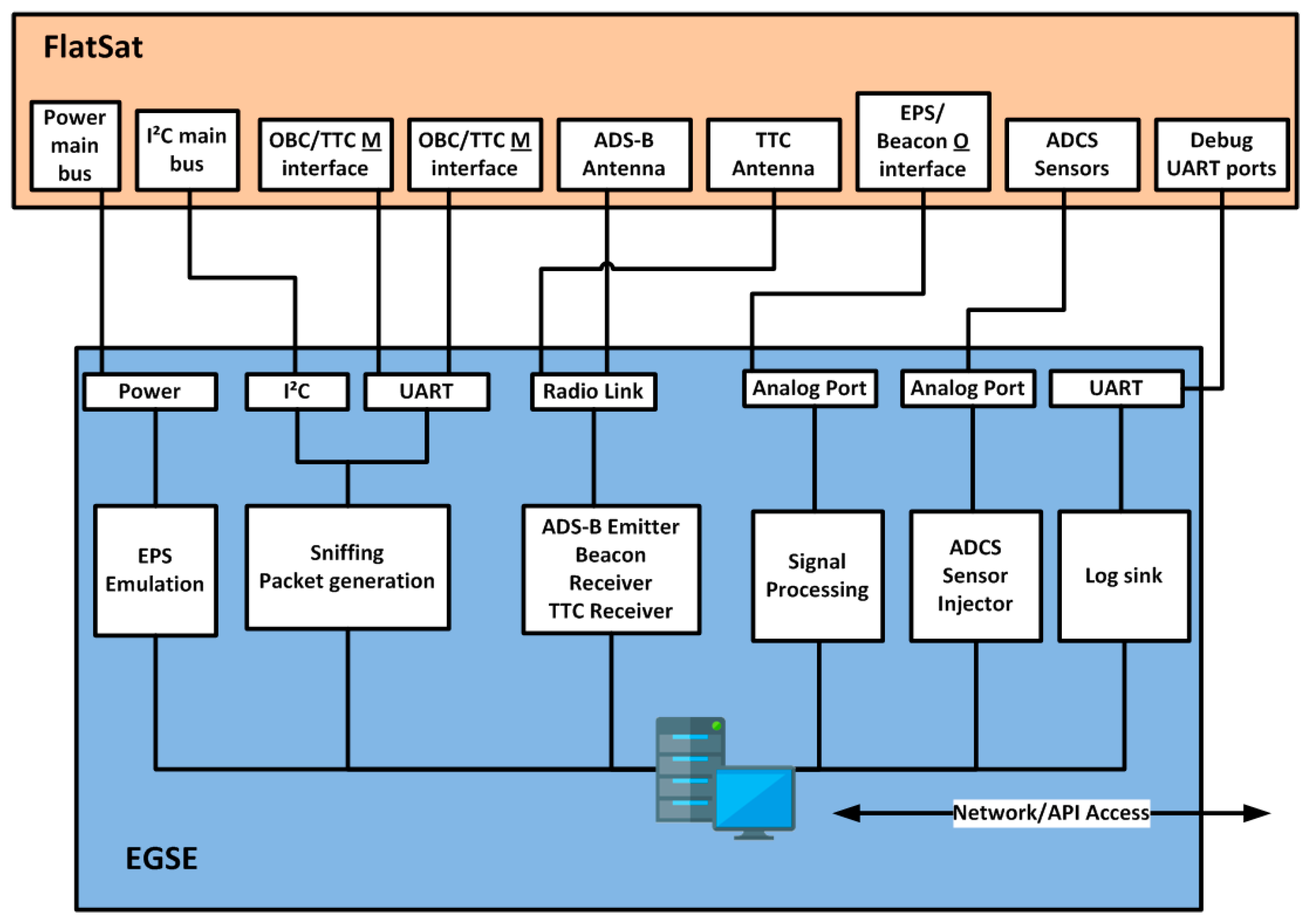
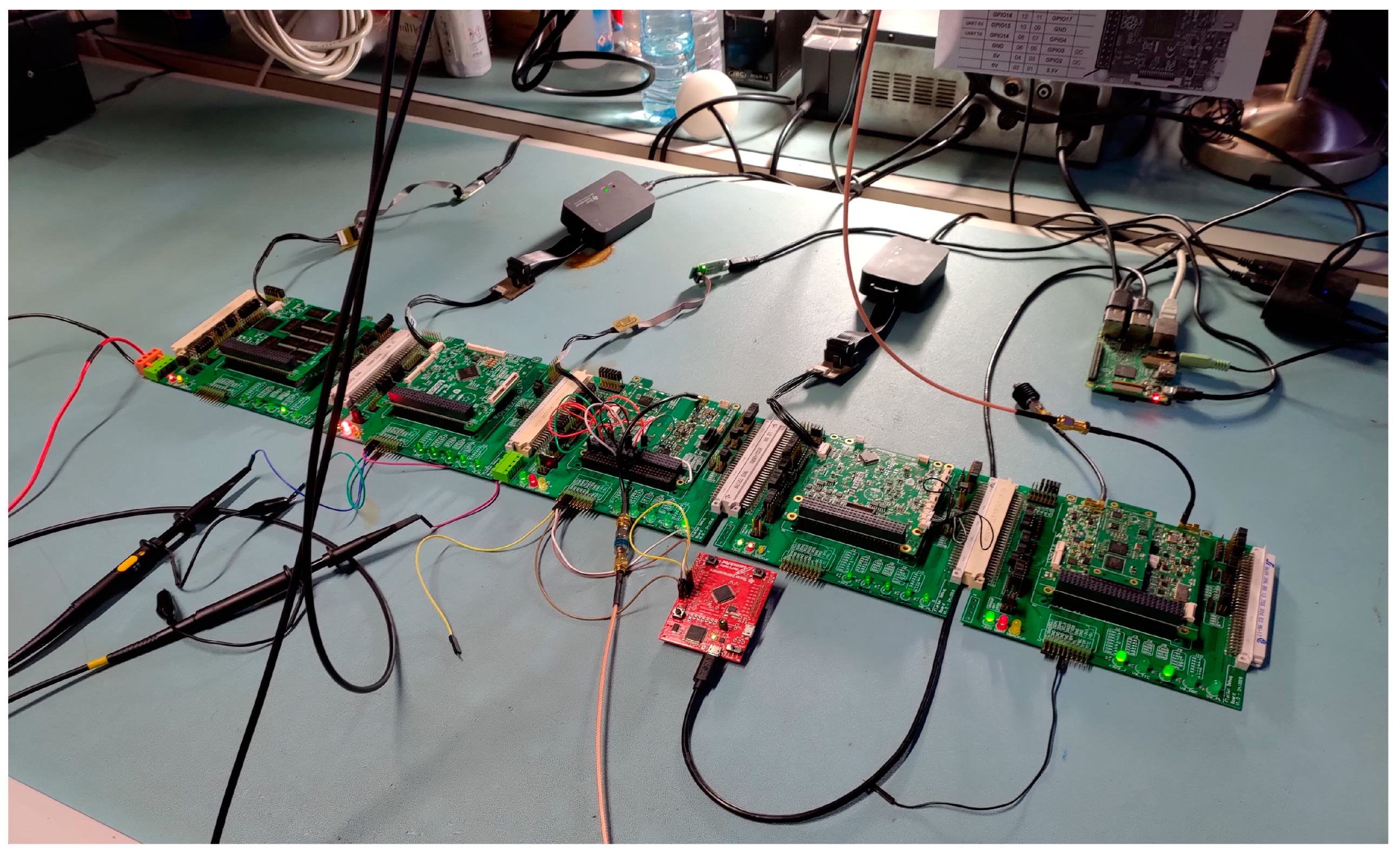
3.1. Flatsat Testing

The unit and integration tests are an ongoing effort, with no tangible results to be presented other than code coverage and test failure statistics. They are used more as a development tool than as a typical verification and validation tool. Nonetheless, the framework will be very useful for formal functional testing, during which the full functionality of the spacecraft will be tested.
Regarding I2C interface characterization, some results can be presented. Due to the AX.25 maximum payload and upper layer protocols, an ISTNanosat Control Protocol (INCP) message has a maximum size of 245 bytes in the radio link. Since messages received from the ground can be forwarded from the OBC and COM to other subsystems, and vice versa, in order to avoid fragmentation, all interfaces and protocols need to support a payload of 245 bytes. As can be seen in Table 3, this is verified for every subsystem.
In ideal conditions, that is, when there is only one transmitter and one receiver, no message loss is expected. While characterizing the I2C interface, one test was to perform 100 pings, i.e., sending a message to a subsystem that triggers a one-message reply. Table 3 shows that no messages were lost under these conditions.
While a strict requirement regarding return trip time (RTT) does not exist, a value above 25 ms is indicative of a problem. The RTTs for all subsystems fall below this soft limit, although there’s a significant difference between them. For example, the EPS has an RTT that is almost four times larger than the TTC. This is explained by the combination of the different processing powers of the microprocessors and differences in the implementation of each subsystem.
Finally, a throughput test was performed. While receiving, all subsystems handled the 10 KB/s throughput (after considering protocol overheads) supported by the link. However, not all subsystems can produce and transmit messages fast enough to use the link’s full potential. In particular, there are systems such as the EPS and the TTC from which it was not possible to collect data leading to a result with statistical relevance.
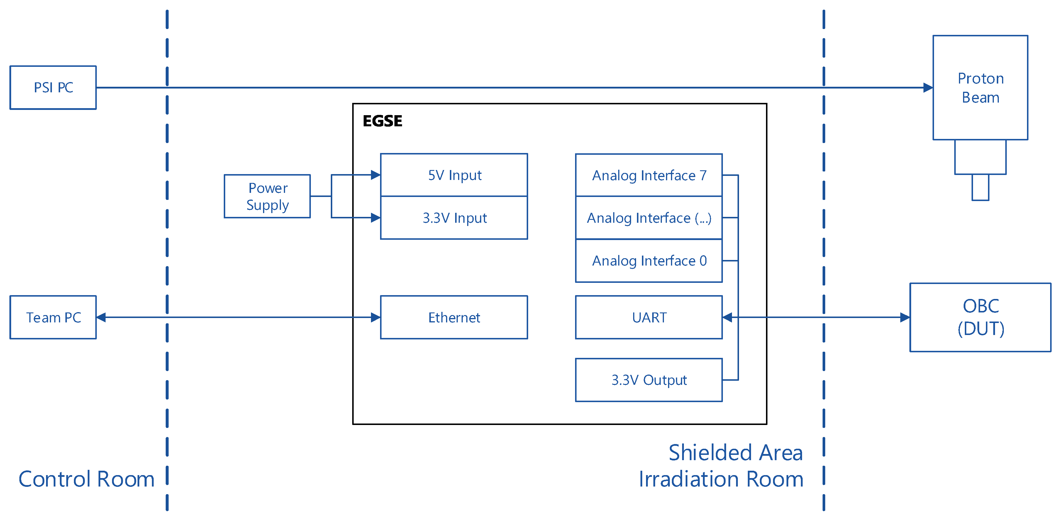
Communications to and from the ground are ensured partly in the TTC and partly in OBC. The result is a suit of tests to ensure that the TTC can send and receive data from the ground by confirming the transmission and reception of messages via the ground station; the ability to change parameters; and that the specified data that should be available through this interface is indeed available. As these tests have a go/no-go nature, there are no statistics concerning the protocol performance except for the number of requirements covered by these tests. Up to now, all the basic communication requirements are covered.

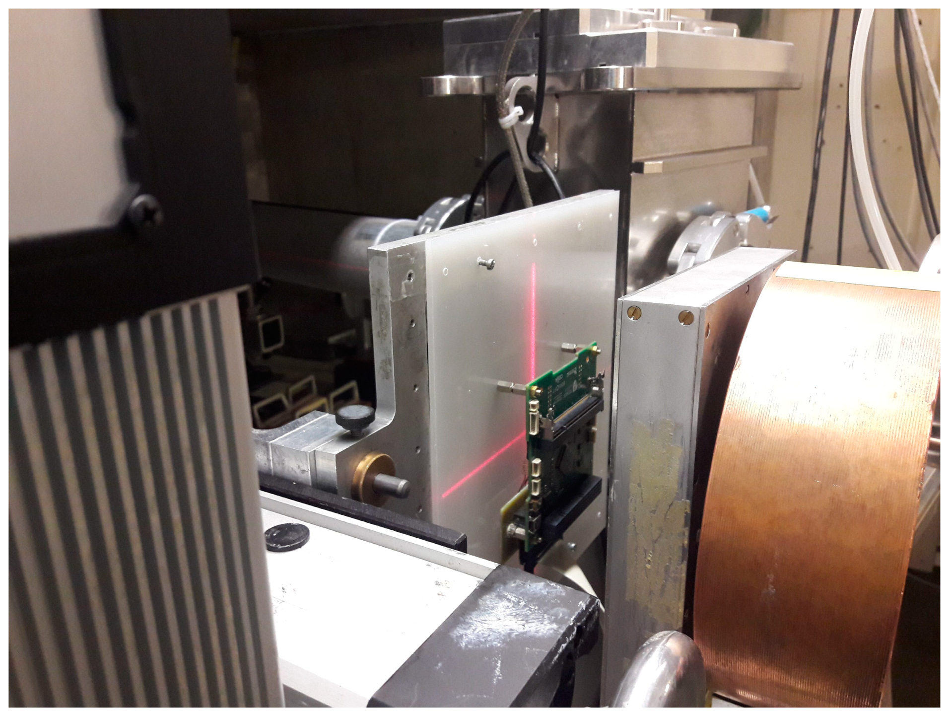
3.2. Ionizing Radiation Testing

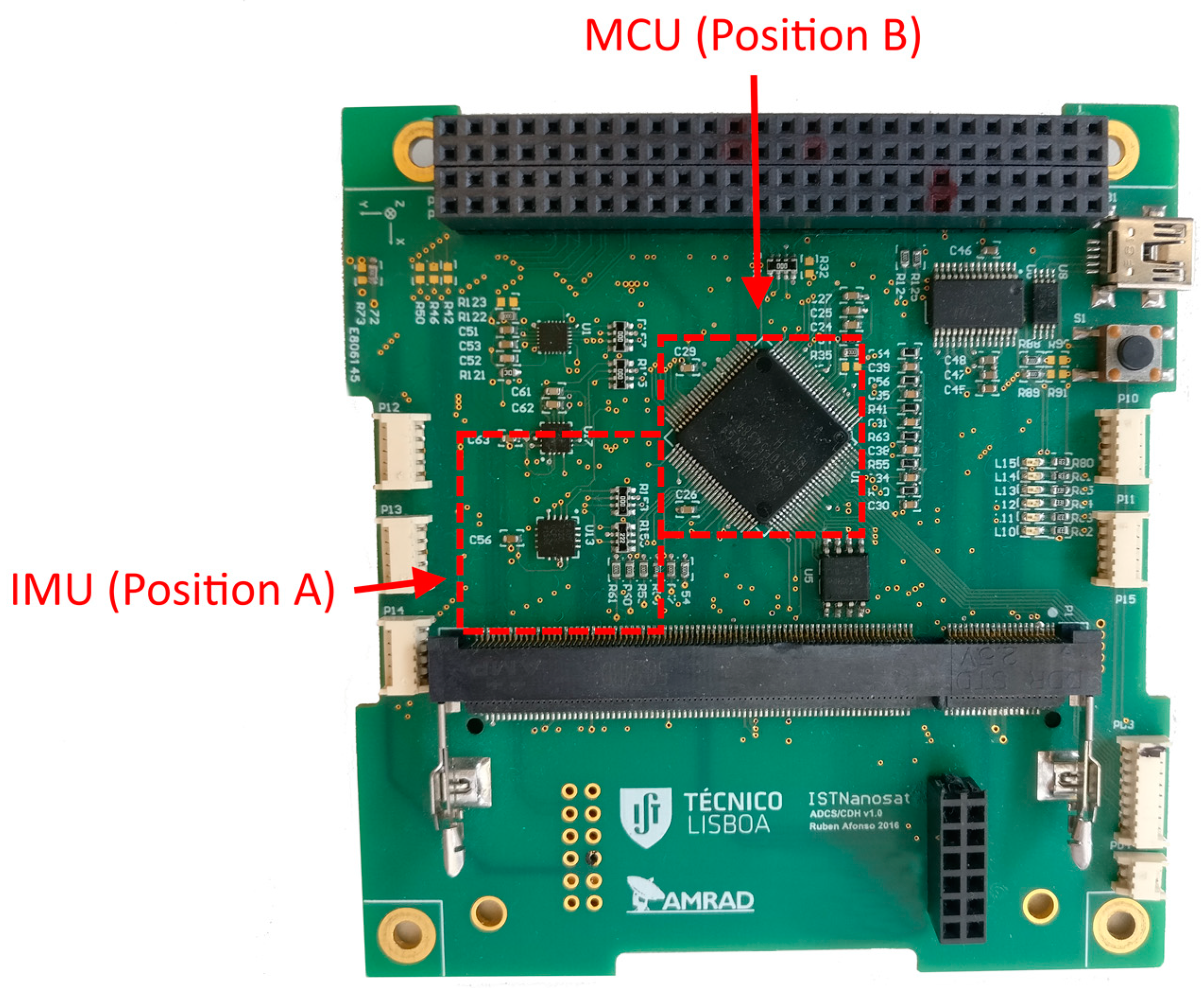
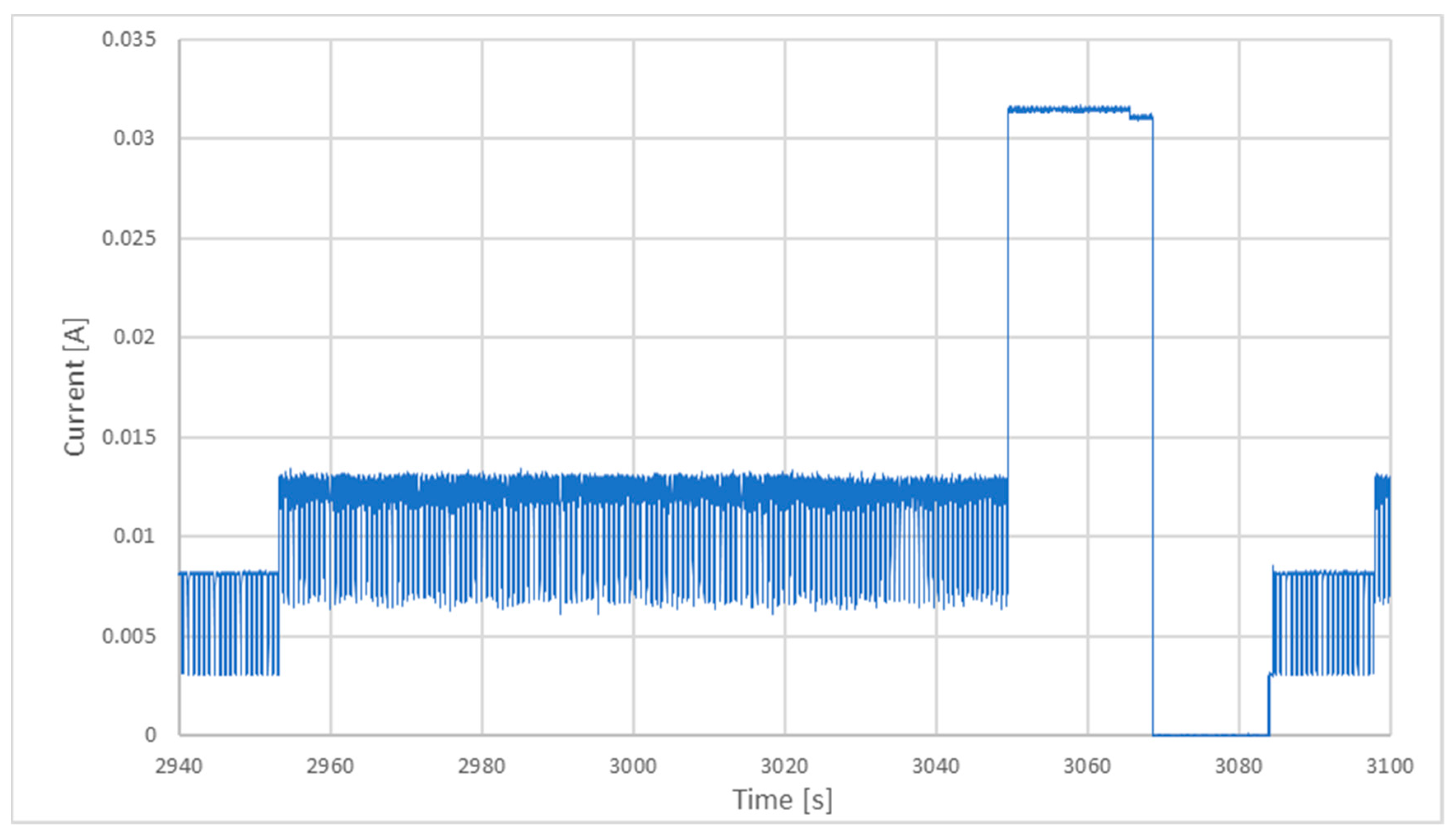
During RUN1, the observed anomalies were related to the sensor directly in the path of the beam, the IMU. The MCU detected four overcurrent events in its power rail, and each time, the software automatically disconnected it. The same anomaly occurred only once during RUN2 when the flux was increased. On RUN3, a small current draw increase on the IMU, from 8 mA to 13.4 mA, was detected at 2953 s (Figure 16). The MCU did not respond to this increase since it was still below the cutoff value. The current was maintained for 96 s until 3049 s, when the current reached 31 mA, which was a value above the threshold, and the MCU turned it off.
After restarting the sensor at 3084 s, it started working normally, but the current increased to the same level, 13 mA, after 14 s. In RUN6 (runs 4 and 5 were aborted due to a problem in the beam), during which the beam was not focused on the sensor, the current draw was 8 mA. It is probable that the incident radiation changes the behavior of the sensor, but it is not enough for it to stop working.
In RUN7, the EGSE stopped running after 60 s and could not be restarted from the control room. The beam was stopped, and a power cycle to EGSE was applied in the chamber. It was discussed that without the collimator to focus the beam, more protons were dispersed and probably interfered with the EGSE, blocking the MCU in a state that could not be recovered remotely.
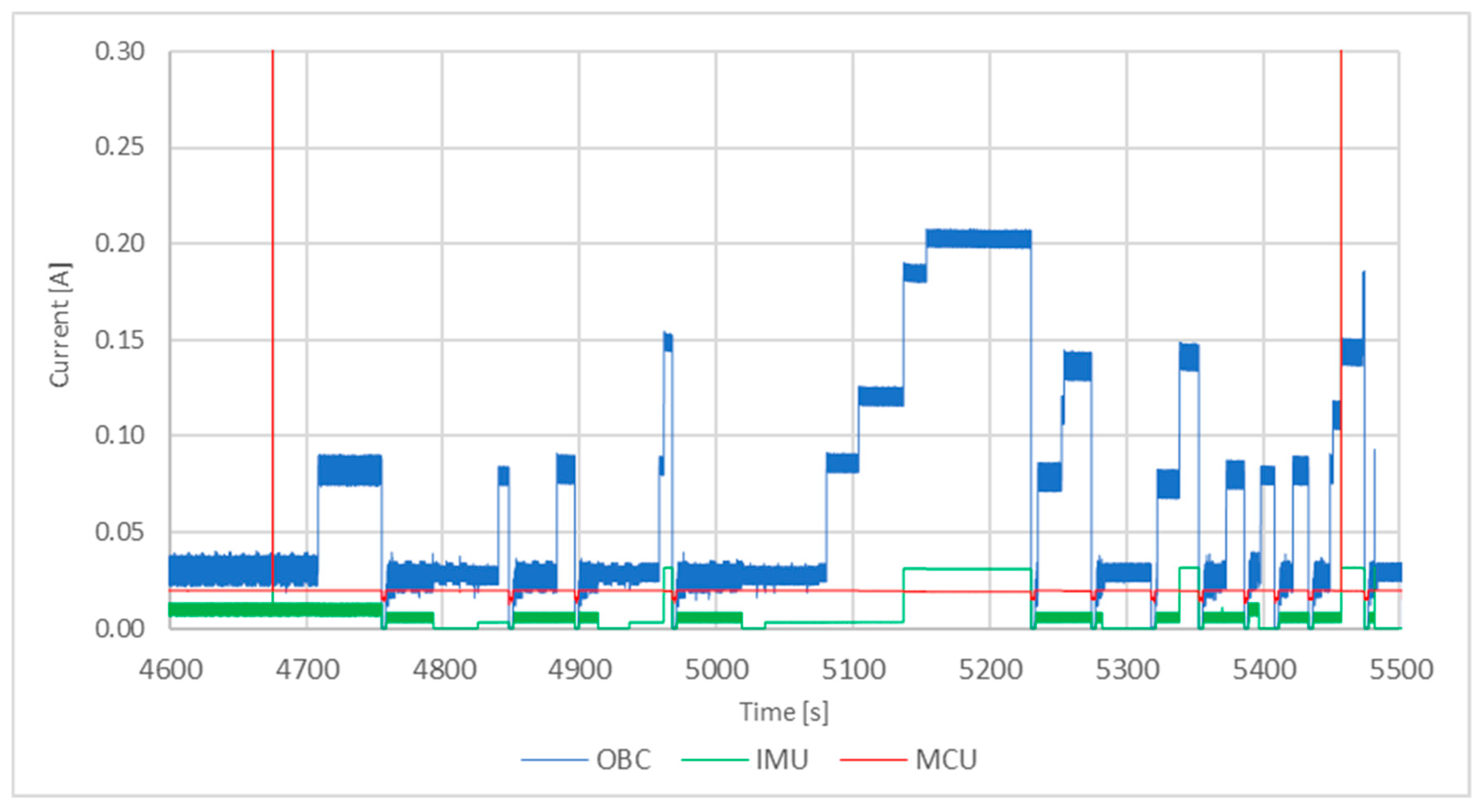
In RUN8 (red spikes at 4675 s and 5457 s on Figure 17), the MCU’s current reached 315 mA, forcing the EGSE to cut off its power rails. There were situations in which the overall current increased, but the MCU current remained constant. The team’s interpretation was that some component on the board was affected, but the MCU was not directly affected. The MCU may lock up from a condition originated by a component or peripheral in an unexpected state.
At 5080 s, the OBC was left on to see what happened if the current increased. The current increased four times but never reached the 300 mA threshold to force a shutdown. At 5352 s, when the flux increased, the time between failures decreased as expected. Finally, at 5449 s, with the maximum flux of 8 × 10⁻⁷ p/cm2/s, the same four steps happen, but faster, in only 12 s. After a reboot, and without the beam, the system recovered its normal operation. In total, more than 15 manual power cycles were executed to gain control of the system. In all of them, the MCU lost the communication with the EGSE in less than 30 s.
The results show that, as predicted, the current draw from the individual components (sensors and MCU) greatly increases in the presence of high-energy particles—which build up charges on electronic devices when passing through them. The most affected devices are transistors (and any device that makes use of them), since their operation is based on changing charges. If the state of the transistor changes, it may allow current to flow, increasing the overall current consumption. At the levels used for the test, this effect is almost immediate, taking less than 30 s before the current level reached the threshold. The test showed that this effect does not permanently damage the sensors if appropriate action is taken, and the system is powered off. Therefore, the test increased the confidence in the design tolerance to radiation-related faults. The current overload detection mechanism was changed by implementing a time-averaged current draw threshold in addition to the already used instantaneous threshold. This way, the system can detect if there is a rapid current spike and a slow increase in current over time. These two methods also were implemented in the EPS subsystem.
As a direct consequence of the test, an external watchdog to the OBC MCU was added in order to force a restart in case of a latch-up. The software configuration was also changed to allow easily turning the internal Watchdog Timer (WDT) on/off during compilation using flags. These design changes are not foreseen to be tested again under the same environmental conditions unless a similar opportunity is offered. However, both changes are going to be tested as part of the functional test campaign, which will be run at ambient temperature and pressure. It is important to note that the addition of the external watchdog would likely have required the development of new flight hardware had the test only occurred after PFM integration.

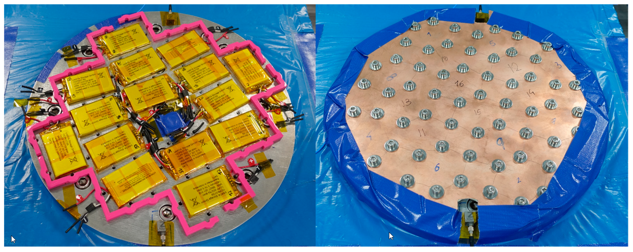
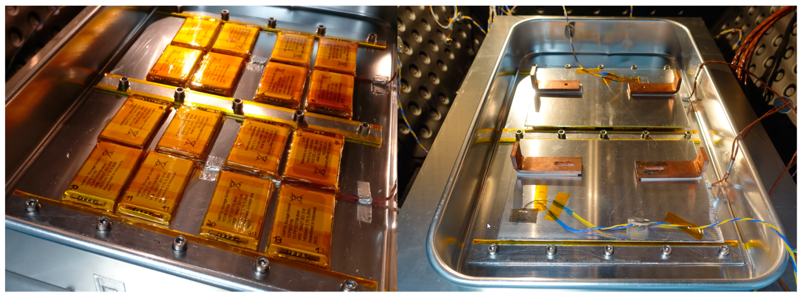
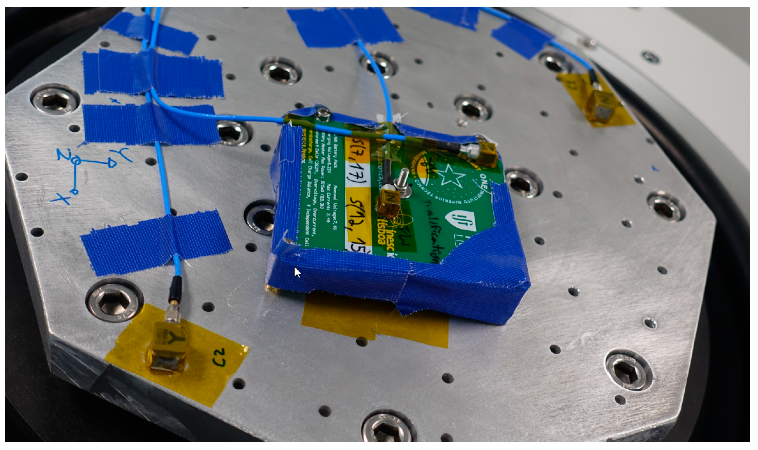
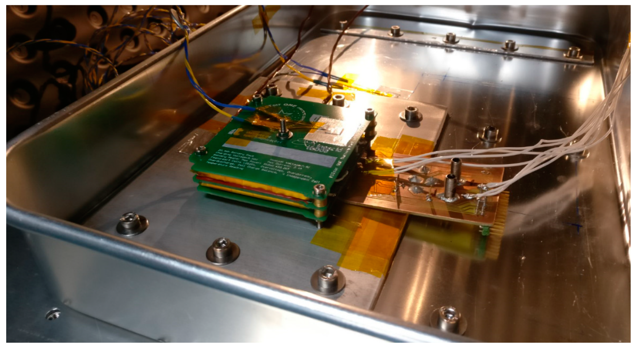
3.3. Battery Qualification Campaign

The physical and electrochemical characterization of the cells demonstrated that all 16 cells to undergo acceptance testing were compliant with the manufacturer datasheet. Cell discharge profiles were very similar for all cells.
After verifying their correct characteristics, all 16 cells endured the vibration test with no incidents. Each cell was vibrated in three different orthogonal directions and with a random mean square (RMS) acceleration of 9.65 g (the test logs demonstrate this but were excluded from this article due to size). Between each run, the cells were checked for both internal resistance and open circuit voltage. In all health checks, the cells revealed that they were not affected by the vibration tests.
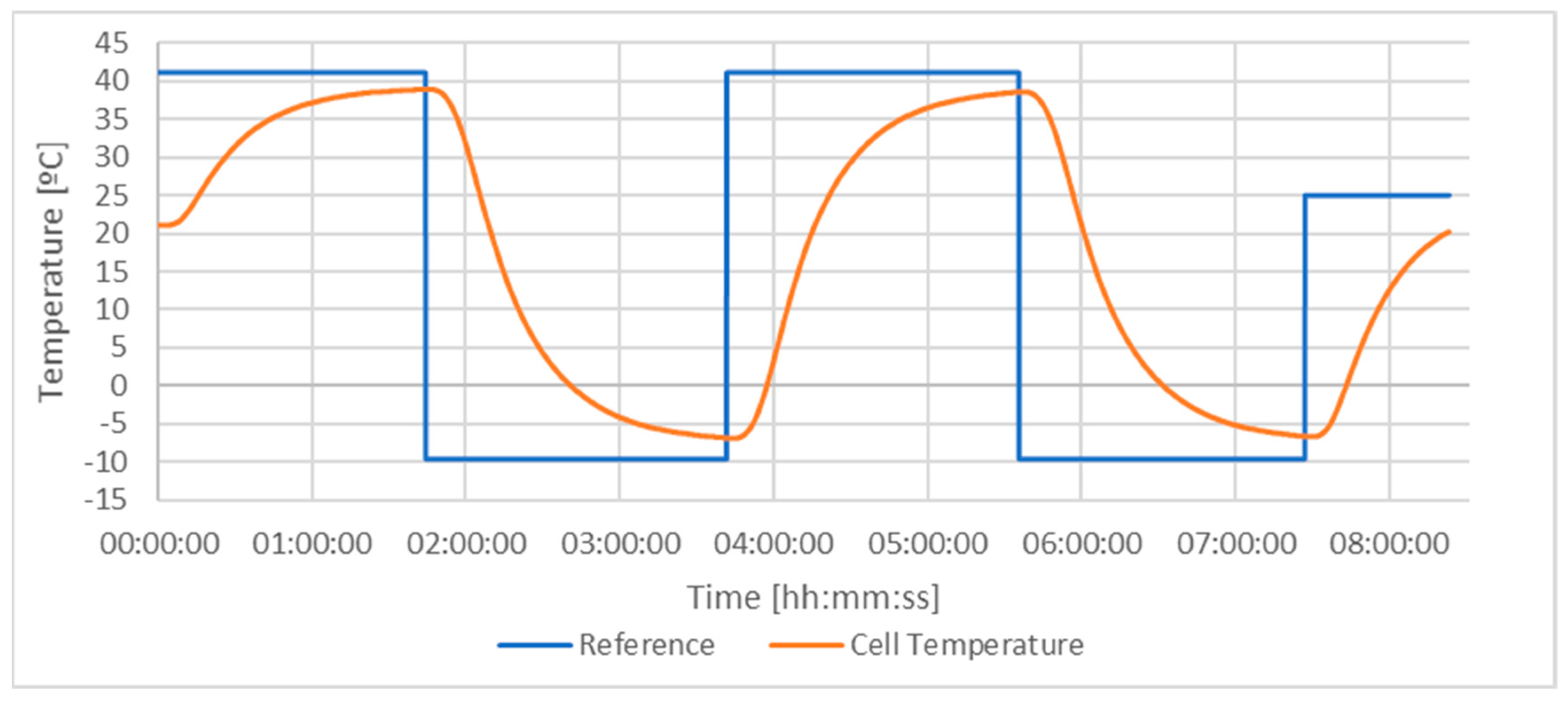
Regarding the TVAC test, all cells faced temperatures from roughly −9 °C to +39 °C under vacuum conditions (as seen in Figure 18) without any incidents. The cells were submitted to, and survived, more than 10 h at a pressure of less than 10−6 mbar. The tests did not harm the cells, as demonstrated by health check tests.
Reassessment of the cells’ physical and electrochemical characteristics demonstrated that all survived the tests. The mean relative discrepancy between pre-test and post-test internal resistance was +1.27%, with a standard deviation of 2.01%. The mean relative discrepancy between pre-test and post-test discharge capacity was +1.03%, with a standard deviation of 2.12%. In both cases, the deviation was positive, which is counterintuitive—capacity should decrease with every discharge cycle, particularly under stress conditions. The team attributes this to measurement error due to different environmental conditions between pre-test and post-test characterization, as cell internal resistance and capacity vary significantly with ambient temperature. Therefore, the team concluded that the cells were not damaged during acceptance testing.
The qualification battery model was assembled, and characterization tests were performed. The battery tester was configured to discharge at a current of 800 mA (0.3 C) and let the battery discharge until the voltage dropped to 6.2 V or the current dropped below 700 mA. The battery pack was charged up to 8.3 V before starting the procedure. The total discharge capacity under these conditions was 2576 mAh.
Having confirmed the nominal operation of the battery pack, electrical stress tests were performed. The first test was the undervoltage test, which was performed also at an increased discharge rate (1.5 A, or 0.6 C). The cell protection circuit cut power at a battery voltage of 4.57 V, with the first cell to engage the protection circuit at 2.285 V (The protection circuit acts at an individual cell level. The total battery voltage was 4.57 V due to the series association of two cells at roughly 2.28 V). The manufacturer datasheet states 2.3 V as the minimum voltage below which the protection circuit is engaged, which means that this test yielded slightly worse results than expected; however, they were well within the 5% established tolerance. Under these conditions, the total discharge capacity was 1634 mAh, which was 37% below nominal conditions. This performance penalty was expected and is in line with the manufacturer datasheet.
Then, the battery was charged at a rate of 0.3 C, and the overcharge protection circuit was tested. The system engaged at a battery voltage of 8.572 V (about 4.286 V per cell, which is very close to the manufactured specification of 4.275 V for overcharge protection engagement), thus proving that the battery was adequately protected from overcharge and undercharge.
The final electrical abuse test was an external short-circuit test. The positive and negative pads were shorted, and the protection circuit engaged after 5 ms when the peak current was 8.44 A. The test showed that even in the event of an external short circuit (for instance, a piece of debris shorting the battery terminals) or a software glitch that would allow the EPS to overcharge or undercharge the battery, the passive battery protection circuit is capable of preventing any situation that could lead to a defective lithium polymer cell.
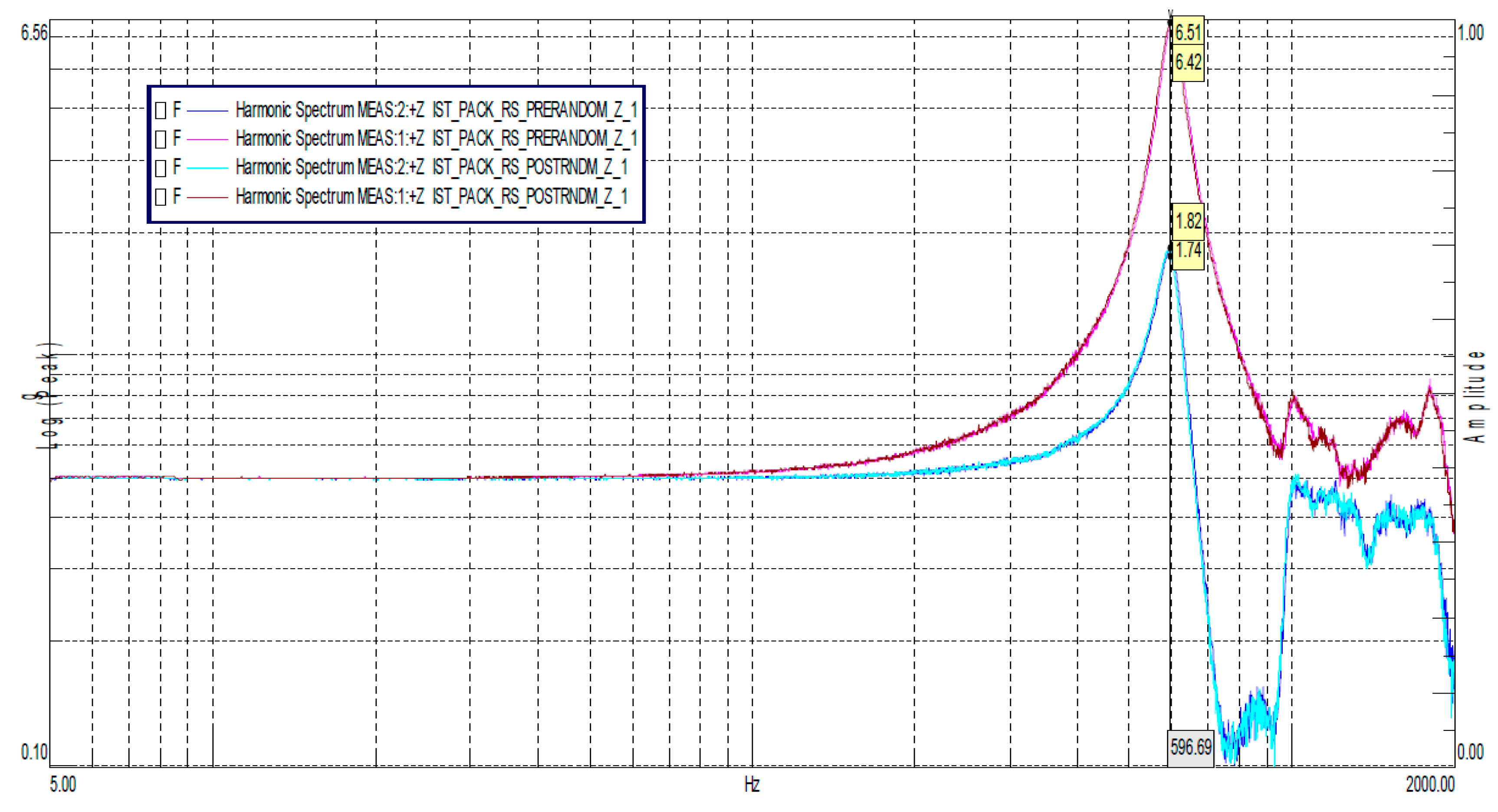
The team returned to the CSF in order to perform vibration and TVAC testing. The battery pack endured the expected random vibration profile (with a 13.65 g RMS acceleration) on all axes for a total duration of 5 min each. Before and after each random vibration test run, a low-level sine sweep was performed in order to assess the frequency response of the battery. In all cases, the frequency and amplitude shift in both accelerometer measurements were below 5%, demonstrating the adequate structural design of the battery pack. An example can be seen in Figure 19, which shows that the frequency response curves for the accelerometer near the edge (blue lines) and near the center (pink lines) before and after the tests are nearly overlapping, indicating that no structural degradation took place. Electrical characterization before and after the test also confirmed that the battery had suffered no performance degradation.
After the random vibration test, the TVAC test took place. The initial OCV was 8.111 V, and the goal was to discharge at 0.8 C until 70% depth of discharge (DoD) corresponding to an expected 1960 mAh discharge capacity. At 60 °C, the time elapsed was 1 h 46 m 21 s, reaching a final voltage of 6.382 V and a total discharge capacity of 2021 mAh. This increase is expected due to the reduction of the cells’ internal resistance at higher temperatures.
Charging took place at 40 °C and a 0.5 C charge rate. The initial voltage before charging was 7.491 V, the final voltage was 8.246 V, and the maximum charging current was 0.727 A. After 20 min, the voltage settled to 8.158 V.
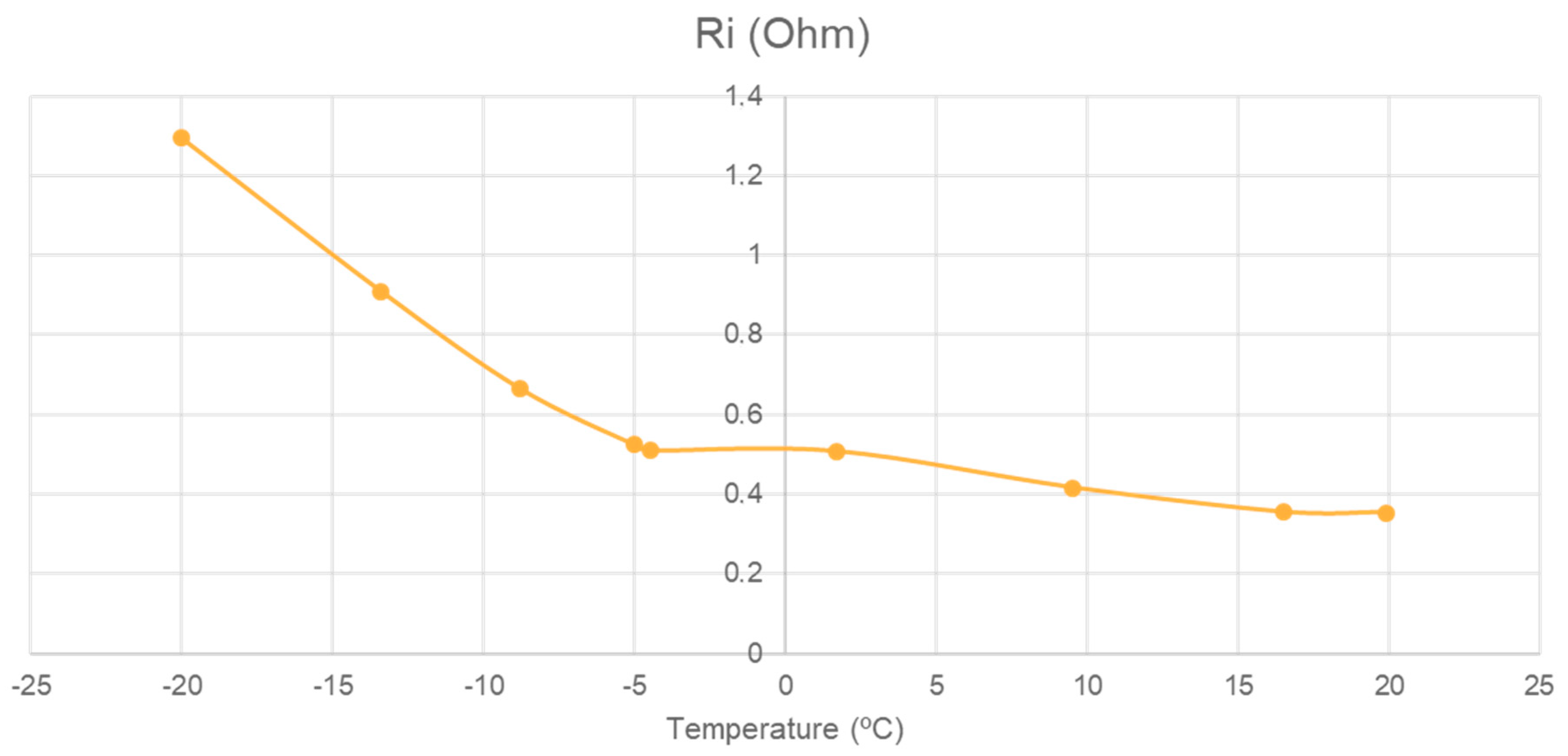
Then, the chamber was set for −20 °C and dwelled at this temperature for 2 h. The first attempt at discharging the battery was aborted, because the voltage drop under the nominal load was excessive at 700 mV, resulting in a 1.2 V decrease in less than one minute. Due to this unexpected behavior, the team decided to raise the temperature to −5 °C in order to understand if the damage was permanent or if it was induced by the low temperature. While the chamber temperature increased, the OCV and internal resistance were monitored in order to assess whether it was safe to perform another discharge. As shown in Figure 20, as the temperature increases, the internal resistance decreases. This test demonstrated that despite the manufacturer claiming operability at −20 °C, the internal resistance at this temperature is too high, and therefore the discharge capacity is too low.
The discharge test took place at −5 °C. As expected, the performance degraded when compared to the 60 °C discharge profile, with a total discharge capacity of 1503 mAh, a final voltage of 6.498 V, and a total time of 1 h 25 m 40 s.
The final charging of the battery took place at 0 °C, resulting in a charging capacity of only 1020 mAh, which was expected as the charge rate was higher in order to reduce the charging time (1 h 46 m 33 s).
Physical and electrochemical characterization of the battery pack at the end of the campaign showed that the overall performance of the battery pack degraded by 99 mAh—specifically to 2477 mAh, a 3.5% capacity loss, which is within the error margin. The internal resistance at 100% state-of-charge was the same, 152 mΩ. This means that the battery recovered from the thermal vacuum incident that occurred during the discharging process at negative temperatures, and that the qualification campaign, which featured abuse testing at levels quite above expected nominal conditions, did not degrade the battery. Overall, the conclusion was that the battery is safe and its protection circuitry is adequate, but that the team needed to reassess the mission profiles and the battery heater duty cycle in order to prevent discharging at negative temperatures.

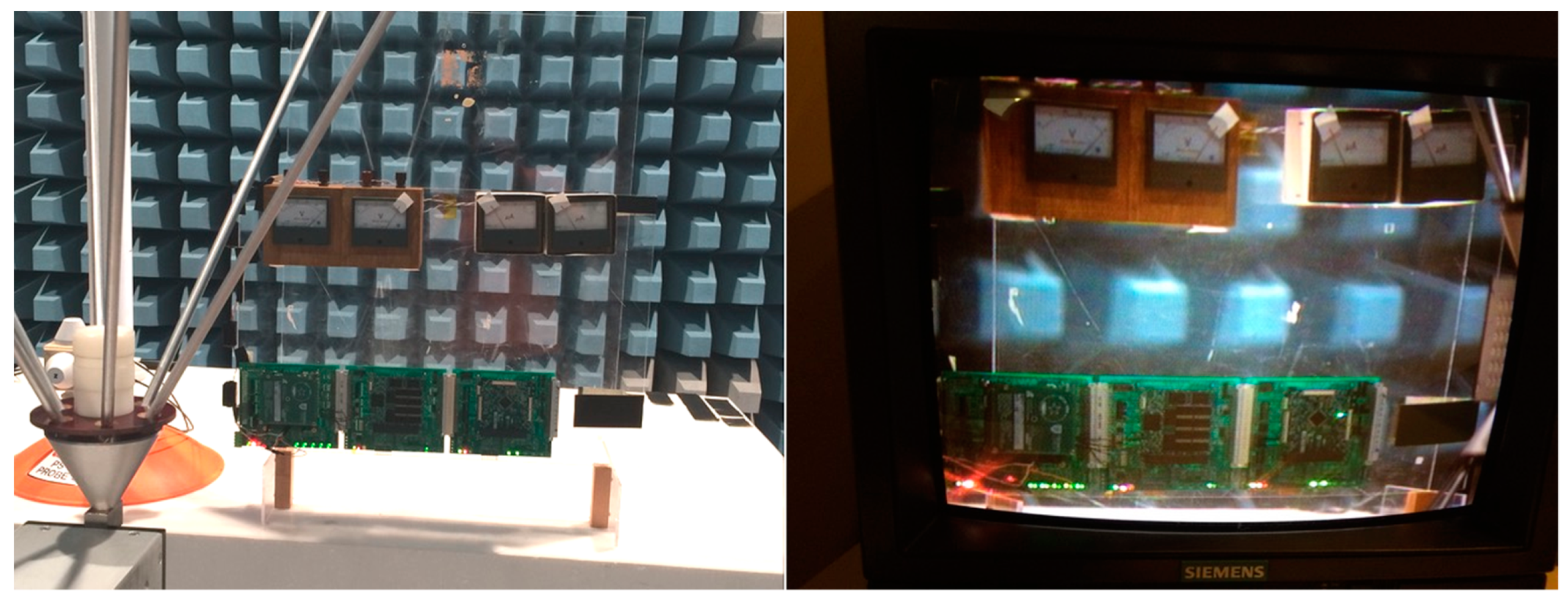
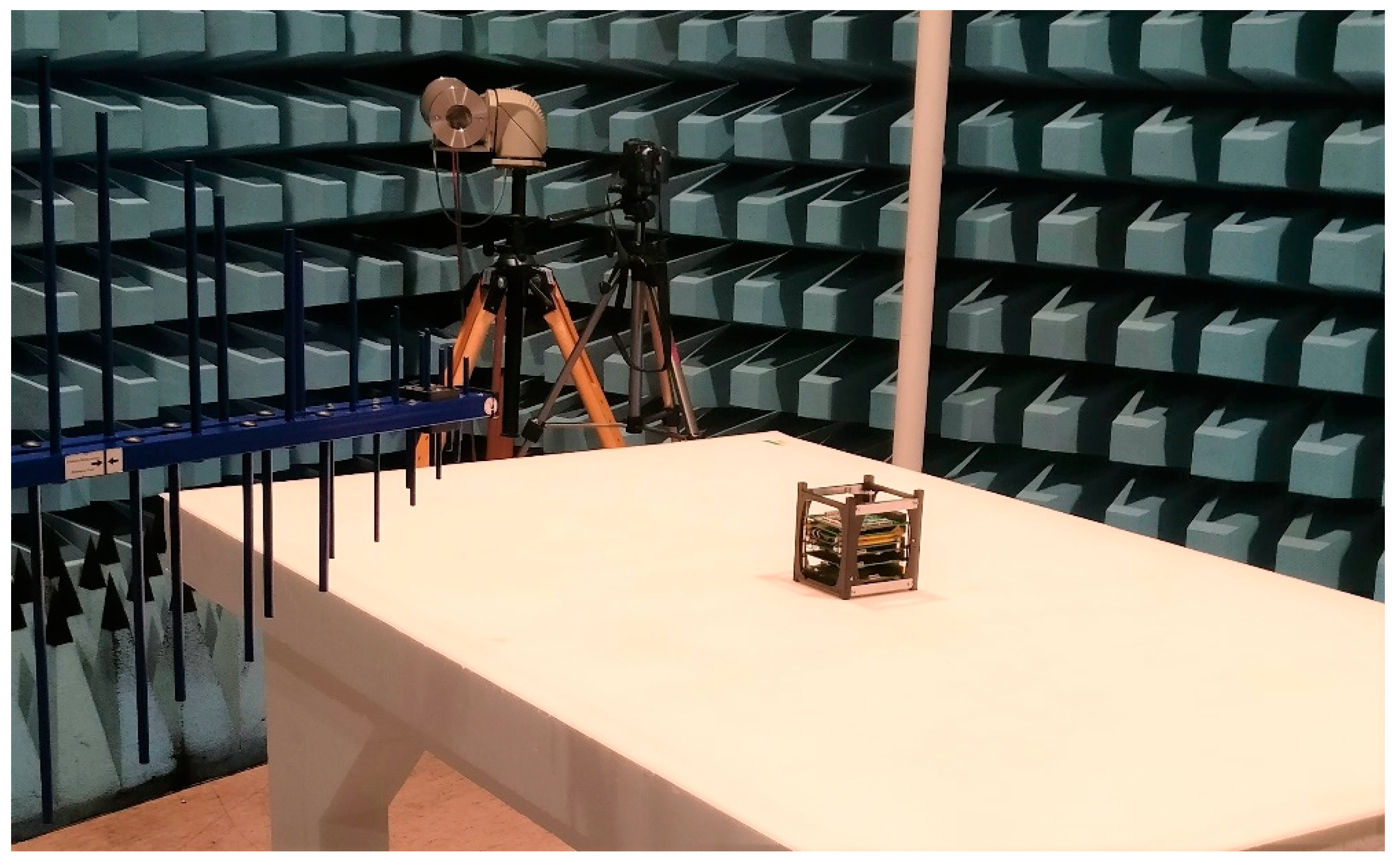
3.4. Electromagnetic Compatibility Testing

The first two immunity testing runs were executed without problems, but the third revealed a malfunction of the OBC, which occurred at 63 MHz with an illuminating field of 10 V/m. A quick diagnostic revealed that the RF radiation was being injected into the unprotected cables connected to the voltmeters and ammeters and consequently affecting the quality of the subsystems’ power lines. Due to this problem, the test procedure was interrupted so that the test setup could be improved. The cables were better twisted and relocated on the supporting panel along with the addition of ferrite cores over the cables. Following this rearrangement of the panel wiring, run 3 was repeated. On all runs, the DUT did not malfunction i.e., the current and voltage levels were constant, and the software ran with no issue. Three more runs were carried out with the boards in the stacked configuration. As before, the results were positive without any change in the behavior of the DUT in the whole frequency range used.
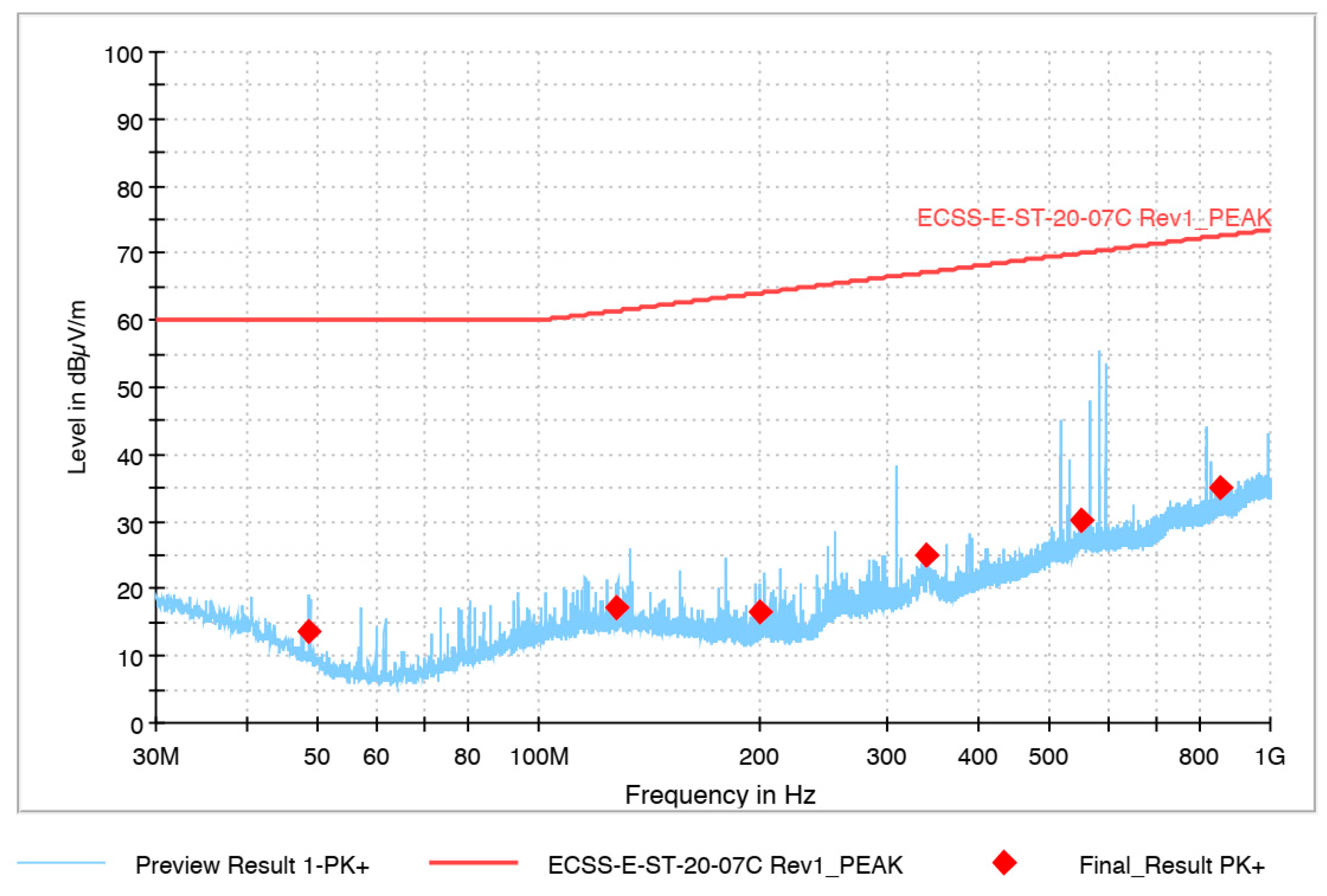
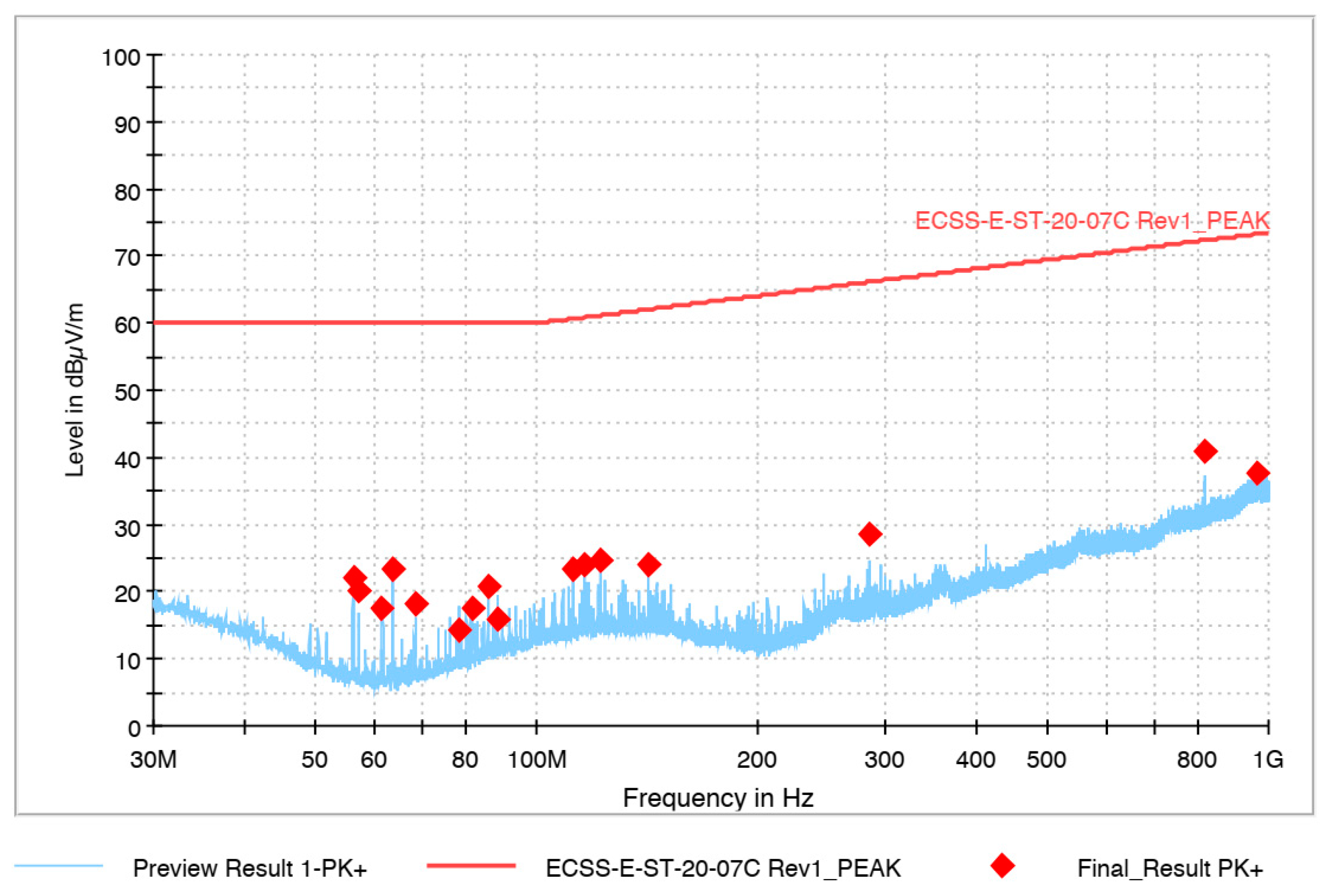
Regarding emission testing, in the first phase only the EPS, OBC, and COM were assembled in the structure. The intention was to check the amount of radiation generated essentially by the processors. Next, the payload was added, and the result compared with the previous values. A total of 12 runs were performed, six for each polarization, and covering the six faces of the S/C. The result of this first phase was very encouraging, as the maximum detected radiation peaks, mainly in the 80 MHz zone and corresponding essentially to the activity of the processors running an external memory test (activity on the processor external bus), were always below the limit set by the standard (receiving antenna 1 m from DUT), as seen in Figure 21. The contribution of the ADS-B board to the overall radio noise of the satellite was not significant.
In the second phase, now with the satellite equipped with its five subsystems and the RF output of the TTC terminated in a 40 dB attenuator, the radiation emitted by the system was re-analyzed throughout the system across the entire frequency band. In this test, the contribution of the TTC to the satellite-radiated field was evident, with some peaks at certain frequencies (harmonics of the emission frequency and signals generated internally), although the maximum values were still 20 dB below the limit defined in the standard (as seen in Figure 22). The TTC continuously emitted a test signal, and although terminated, there is still a small portion of that signal that is radiated outwards by the plugs and cables connected to the load.

4. Discussion

The ISTSat-1 team opted to develop most of its CubeSat subsystems, a decision which involved more risk considering the team’s lack of experience. In order to mitigate this risk, an “agile” approach to AIV activities was proposed in order to incrementally add functionality to the system and continuously and iteratively test it. A collection of tests was specified that took advantage of this iterative development process, starting with the development-oriented flatsat tests, and addressing in subsequent stages specific subsystem functionalities of key importance for the overall mission of the spacecraft.
The testing of functional prototypes at an early development stage led to uncovering system-level errors. Flatsat integration uncovered multiple bugs that required design adjustments (most of which were not reported in this article). During the ionizing radiation test campaign, the system’s resilience to permanent damage from single-event effects was demonstrated, but some design changes were required in order to consider not only current spikes but also time-averaged power draw increases. An external watchdog timer was also implemented in the OBC to prevent a combination of faults from latching up the S/C (before the test, the EPS was the only system that could force a reset of the OBC, but if the EPS microcontroller were also faulty, the S/C would remain indefinitely latched up). During the battery test campaign, despite good overall results, the team needed to reassess the battery heater duty cycle due to the limited discharge performance at negative temperatures.
It is important to stress that the insights gained from the early tests described in this work would have been more difficult, if not impossible, to gain during the subsystem development phase of a project employing a traditional “stage-gate” process, under which integration testing would take place only after each individual subsystem was verified against its requirements and therefore no system-level problems (such as interface issues, electromagnetic noise, and current draw fluctuations) would surface. While some issues were uncovered that only affected one subsystem, many arised from the interactions between subsystems. In addition, not all the tests were initially foreseen in the ISTSat-1 AIV process, due to lack of funding and/or availability of test facilities, but having working prototypes (even if not fully functional) of the subsystems early on meant that the test opportunities sponsored by the team’s partners could be accommodated when made available.
As a conclusion, the team considers the iterative development and testing approach to be useful for educational projects that employ a small, co-located team with low non-recurring engineering costs and is confident that early testing will clear the way to a successful protoflight qualification of ISTSat-1, which is foreseen for 2020. Further application to specific projects is required for extrapolation to environments other than educational projects, but the team’s experience showed that relevant design flaws can be uncovered from the integration of quickly and cheaply prototyped mockups, perhaps more effectively than through extensive analysis and simulation.

Author Contributions

J.P.M. and R.M.R. organized, wrote, and revised the article, and specified and carried out the battery qualification campaign and the EMC testing campaign, respectively; A.S., R.A. and N.R. carried out and drafted reports for the flatsat, radiation, and battery testing campaigns, respectively.

Funding

This work is funded by FCT/MCTES through national funds and when applicable co-funded by FEDER—PT2020 partnership agreement under the projects UID/EEA/50008/2019 or R&D Unit funding for year 2020.

Acknowledgments

The authors wish to acknowledge contributions from the ISTnanosat team at Instituto Superior Técnico, particularly students João Pinto, Fabian Näf, Afonso Muralha and Luís Ferreira, and supervisors Gonçalo Tavares, Moisés Piedade and Carlos Fernandes. The authors also thank ESA Education for sponsoring the battery qualification and ionizing radiation testing campaigns under the Fly Your Satellite! program, as well as ANACOM for sponsoring the EMC testing campaign and the Portuguese Quality Institute (IPQ) for sponsoring laboratory equipment calibration and certification. Lastly, the authors wish to acknowledge the support of INESC-ID, Instituto de Telecomunicações and Caixa Geral de Depósitos throughout the project. The authors also wish to thank the reviewers for their comments, which led to the improvement of this article.

Conflicts of Interest

The authors declare no conflict of interest.

Abbreviations

ADS-BAutomatic Detection Surveillance Broadcast
ADCSAttitude Determination and Control System
AIVAssembly, Integration, and Verification
APIApplication Programming Interface
CIContinuous Integration
COMCommunications processor
COTSCommercial Off-the-Shelf
CSFCubesat Support Facility
DoDDepth of Discharge
DUTDevice Under Test
ECSSEuropean Cooperation for Space Standardization
EGSEElectrical Ground Support Equipment
EMCElectroMagnetic Compatibility
EPSElectrical Power Supply
ESAEuropean Space Agency
FYSFly Your Satellite
HILHardware-in-the-Loop
IMUInertial Measurement Unit
INCPISTNanosat Control Protocol
ISSInternational Space Station
I2CInter-Integrated Circuit
LEDLight Emitting Diode
MCUMicro-Controller Unit
MTUMaximum Transfer Unit
NRENon-Recurring Engineering
OBCOn-Board Computer
OCVOpen Circuit Voltage
PCBPrinted Circuit Board
PFMProto-Flight Model
RMSRandom Mean Squared
RFRadio-Frequency
RTTReturn Trip Time
S/CSpacecraft
SDRSoftware-Defined Radio
TTCTelemetry, Tracking, and Communications
TVACThermal Vacuum
WDTWatchdog Timer

References

  1. Kulu, E. Nanosats Database. Available online: https://www.nanosats.eu/index.html (accessed on 29 October 2019).
  2. Bouwmeester, J.; Guo, J. Survey of worldwide pico- and nanosatellite missions, distributions and subsystem technology. Acta Astronaut. 2010, 67, 854–862. [Google Scholar] [CrossRef]
  3. Pang, W.J.; Bo, B.; Meng, X.; Yu, X.Z.; Guo, J.; Zhou, J. Boom of the CubeSat: A Statistic Survey of CubeSats Launch in 2003–2015. In Proceedings of the 67th International Astronautical Congress, Guadalajara, Mexico, 26–30 September 2016. IAC-16-E2.4.5. [Google Scholar]
  4. Corpino, S.; Stesina, F. Verification of a CubeSat via hardware-in-the-loop simulation. IEEE Trans. Aerosp. Electron. Syst. 2014, 50, 2807–2818. [Google Scholar] [CrossRef]
  5. Berthoud, L.; Schenk, M. How to Set Up a CubeSat Project—Preliminary Survey Results. In Proceedings of the 30th Annual AIAA/USU Conference on Small Satellites, Logan, UT, USA, 6–11 August 2016. [Google Scholar]
  6. Ampatzoglou, A.; Kostopoulos, V. Design, Analysis, Optimization, Manufacturing, and Testing of a 2U Cubesat. Int. J. Aerosp. Eng. 2018, 2018, 9724263. [Google Scholar] [CrossRef]
  7. Forsberg, K.; Mooz, H. The Relationship of System Engineering to the Project Cycle. INCOSE Int. Symp. 1991, 1, 57–65. [Google Scholar] [CrossRef]
  8. Cooper, R.G. Stage-gate systems: A new tool for managing new products. Bus. Horiz. 1990, 33, 44–54. [Google Scholar] [CrossRef]
  9. ISIS-Innovative Solutions In Space|The Nanosatellite Specialist. ISIS—Innovative Solutions in Space. Available online: https://www.isispace.nl/ (accessed on 31 October 2019).
  10. AAC Clyde Space|Small Satellite Spacecraft Providers. Available online: https://www.aac-clyde.space/ (accessed on 31 October 2019).
  11. Pumpkin, Inc. Available online: https://www.pumpkinspace.com/ (accessed on 31 October 2019).
  12. Welcome to EnduroSat’s CubeSat Webpage, CubeSat by EnduroSat. Available online: https://www.endurosat.com/ (accessed on 31 October 2019).
  13. Carson, R.S. Can Systems Engineering be Agile? Development Lifecycles for Systems, Hardware, and Software. INCOSE Int. Symp. 2013, 23, 16–28. [Google Scholar] [CrossRef]
  14. VanderLeest, S.H.; Buter, A. Escape the waterfall: Agile for aerospace. In Proceedings of the 2009 IEEE/AIAA 28th Digital Avionics Systems Conference, Orlando, FL, USA, 23–29 October 2009; pp. 6.D.3-1–6.D.3-16. [Google Scholar]
  15. Carpenter, S.E.; Dagnino, A. Is Agile Too Fragile for Space-Based Systems Engineering? In Proceedings of the 2014 IEEE International Conference on Space Mission Challenges for Information Technology, Laurel, MD, USA, 24–26 September 2014; pp. 38–45. [Google Scholar]
  16. Douglass, B.P. Agile Systems Engineering; Morgan Kaufmann: Waltham, MA, USA, 2016. [Google Scholar]
  17. Crowder, J.A.; Friess, S. Systems Engineering Agile Design Methodologies; Springer: New York, NY, USA, 2013. [Google Scholar]
  18. GitLab CI/CD|GitLab. Available online: https://docs.gitlab.com/ee/ci/ (accessed on 31 October 2019).
  19. ADALM-PLUTO Evaluation Board|Analog Devices. Available online: https://www.analog.com/en/design-center/evaluation-hardware-and-software/evaluation-boards-kits/adalm-pluto.html# (accessed on 18 November 2019).
  20. VARTA Design Library 1/LPP 503759 8HH PCM W VKB 56427201020; VARTA: Ellwangen, Germany, 2007.
  21. Russell, S.; Delafuente, D.; Darcy, E.; Jeevarajan, J.; Bragg, B. Crewed Space Vehicle Battery Safety Requirements, JSC-20793 RevD; NASA: Houston, TX, USA, 2017.
  22. Jeevarajan, J.A.; Duffield, B.E. Performance and Safety of Lithium-Ion Polymer Pouch Cells. J. Space Saf. Eng. 2014, 1, 10–16. [Google Scholar] [CrossRef]
  23. Space Engineering—Electromagnetic Compatibility; ECSS-E-ST-20-07C; ECSS: Noordwijk, The Netherlands, 2012.
Figure 1. Nanosatellite and CubeSat statistics (extracted from [1]).
Aerospace 06 00131 g001
Figure 2. “Vee” model for spacecraft development.
Aerospace 06 00131 g002
Figure 3. ISTSat-1 development process.
Aerospace 06 00131 g003
Figure 4. Flatsat plus Electrical Ground Support Equipment (EGSE) architecture.
Aerospace 06 00131 g004
Figure 5. ISTSat-1 flatsat.
Aerospace 06 00131 g005
Figure 6. Centering the device under test (DUT) on the beam area.
Aerospace 06 00131 g006
Figure 7. Beam targets for positions A and B.
Aerospace 06 00131 g007
Figure 8. Radiation test setup.
Aerospace 06 00131 g008
Figure 9. Cell acceptance vibration test setup.
Aerospace 06 00131 g009
Figure 10. Random vibration test profiles.
Aerospace 06 00131 g010
Figure 11. Cell acceptance thermal vacuum (TVAC) setup.
Aerospace 06 00131 g011
Figure 12. Pack qualification random vibration test setup.
Aerospace 06 00131 g012
Figure 13. Pack-level TVAC test setup.
Aerospace 06 00131 g013
Figure 14. Radiation immunity test setup. On the right, the view from the facility’s video system which allowed monitoring the blinking light emitting diodes (LED) and the analog gauges.
Aerospace 06 00131 g014
Figure 15. Emission test setup. The device on the background is the video camera used to monitor the test. The DUT is placed on a styrofoam table.
Aerospace 06 00131 g015
Figure 16. RUN3 IMU power consumption.
Aerospace 06 00131 g016
Figure 17. RUN8 beam on full board.
Aerospace 06 00131 g017
Figure 18. Cell-level TVAC test temperature log.
Aerospace 06 00131 g018
Figure 19. Comparison of low-level sine sweep response before and after random vibration testing. Two pink lines represent response in the center of the battery, and two blue lines represent the response near the edge (close to the fastener).
Aerospace 06 00131 g019
Figure 20. Battery internal resistance as a function of temperature (measured during the test).
Aerospace 06 00131 g020
Figure 21. Emission test with the OBC, EPS, and COM subsystems.
Aerospace 06 00131 g021
Figure 22. Emission tests with all subsystems integrated.
Aerospace 06 00131 g022
Table 1. Description of radiation test runs and levels. IMU: inertial measurement unit, MCU: microcontroller unit.
RunPositionFluence (p/cm2)Flux (p/cm2/s)
1A: IMU1.00 × 10101.05 × 107
2A: IMU1.00 × 10102.11 × 107
3B: MCU1.00 × 10102.11 × 107
6B: MCU4.00 × 1092.11 × 107
7C: Full board1.00 × 10112.11 × 107
8C: Full board1.00 × 10112.11 × 107
4.00 × 10⁷
8.00 × 10⁷
Table 2. Random vibration test levels. ASD: Acceleration Spectral Density.
Freq [Hz]Cell AcceptanceBattery Qualification
ASD [G2/Hz]dB/OctgRMSASD [G2/Hz]dB/OctgRMS
200.0288000.057600
400.0288000.000.760.0576000.001.07
700.0720004.931.430.1440004.932.02
7000.0720000.006.890.1440000.009.74
20000.018720−3.869.650.037440−3.8613.65
Table 3. I2C interface characterization. OBC—on-board computer; EPS—electrical power supply; COM—communications processor; PL—ADS-B payload; TTC—telemetry, tracking, and communications; MTU—maximum transmission unit; RTT—return trip time.
CharacteristicsOBCEPSCOMPLTTC
MTU (byte)245245245245245
Lost Messages (%)00000
Average RTT (ms)11188145
Max Reception Throughput (KB/s)9.959.969.959.899.96
Max Transmission Throughput (KB/s)7.55N/A8.9810.25N/A

