Article

Numerical Simulation of Temperature Distribution in CCD Detector Irradiated by Nanosecond Pulsed Laser

Department of Aerospace and Technology, Space Engineering University, Beijing 101416, China
*
Author to whom correspondence should be addressed.
Aerospace 2025, 12(9), 791; https://doi.org/10.3390/aerospace12090791
Submission received: 17 June 2025 / Revised: 30 August 2025 / Accepted: 31 August 2025 / Published: 1 September 2025

Abstract

A finite element simulation was conducted to analyze the thermal damage caused by a 532nm nanosecond pulsed laser on a CCD detector. A three-dimensional model was developed to study the temperature field variations within the detector. The simulation was centered on the laser-induced temporal progression of thermal damage in the CCD. Results showed that higher laser fluence led to increased heat accumulation, resulting in the expansion of the thermal damage area. Different thermal damage patterns were observed in the light sensor region and the light-shielded region. In the light sensor region, the melting of the silicon substrate expanded more in the transverse direction compared to the longitudinal direction with increasing laser fluence, while damage in the light-shielded region extended from the edges towards the center as laser fluence increased. These distinct damage patterns were attributed to different energy deposition patterns and structural differences between the light sensor region and the light-shielded region.

1. Introduction

The Charge Coupled Device (CCD) is widely used in various applications due to its excellent resolution, sensitivity, and spectral coverage [1]. It is particularly important in applications requiring high imaging quality and detection sensitivity. CCDs are utilized in scientific research [2], industrial inspection [3], medical imaging [4], consumer electronics [5], and also in aerospace. In the aerospace field, CCDs are crucial for tasks such as astronomical observation, Earth observation, and spacecraft navigation [6,7]. However, CCDs are vulnerable to interference and can be damaged by laser irradiation, which can lead to a loss of functionality. Understanding how lasers affect and harm CCDs is essential for maintaining optimal camera performance.
Experimental studies have examined the damage threshold and the effects of parameters such as laser wavelength, pulse width, and repetition frequency on CCD damage. Schwarz et al. studied the influence of laser parameters on CCD damage thresholds, revealing that nanosecond irradiation led to three times higher threshold values for color CCD cameras compared to picosecond irradiation [8,9]. Han et al. conducted damage experiments on a CCD detector using a continuous-wave laser with a wavelength of 1.06 μm and a power density of 5 × 10⁴ W/cm2. They performed detailed analyses of damage stages under varying irradiation durations, encompassing point damage, vertical bright linear damage, horizontal dark linear damage, and complete damage [10]. Zhang et al. examined the interference effects of lasers with wavelengths of 473 nm, 532 nm, and 632.8 nm on CCD detectors, observing increased interference with longer wavelengths due to quantum efficiency variations. They obtained laser-induced crosstalk thresholds for the monochromatic CCD of 0.26 W/m2, 0.19 W/m2, and 0.09 W/m2 under irradiation at 473 nm, 532 nm, and 632.8 nm, respectively [11]. Cheng et al. irradiated the CCD with a high-power continuous-wave laser at 1080 nm wavelength, yielding an experimental damage threshold of 2.13 × 10⁶ W/cm2 [12]. Cao et al. devised a nanosecond/picosecond combined-pulse system and identified short circuits between the silicon substrate and electrodes as the main cause of CCD device breakdown under combined laser exposure [13].
Researchers have also investigated the damage mechanisms of CCD detectors through numerical simulations. Nie et al. developed a 2D axisymmetric finite element model to study the effects of 1.06 μm laser irradiation at different repetition frequencies (1 kHz, 5 kHz, and 10 kHz) on the detector’s thermal damage. Their findings revealed that lower repetition frequencies led to more effective damage under the same average power density conditions [14]. Li et al. proposed a thermal damage model for CCD detectors exposed to high-repetition-rate and high-peak-power lasers, considering thermomechanical coupling effects. The study found that using high-repetition-rate (100 kHz/21.6 W) and high-peak-power (1 Hz/25 MW) lasers together resulted in significantly lower damage thresholds and shorter durations than using each laser type separately [15]. Additionally, a 3D transient model confirmed that heat and thermal stress coupling were the primary causes of CCD damage during millisecond laser irradiation [16]. Zhang et al. performed a theoretical analysis and simulation study on CCD irradiation by a 1.06 μm continuous laser, determining that stress damage preceded temperature damage [17]. Li et al. conducted a finite element simulation to analyze thermal damage in Si-CCDs under millisecond laser irradiation. The study revealed that increasing laser fluence initially led to damage in the color filter layer, followed by microlens melting. Functional damage occurred when channels in the N-Si layer were compromised [18]. Ren et al. developed a model based on thermal conduction-thermoelastic theory for CCD irradiation by a high-repetition-frequency (40 kHz) laser. Their model demonstrated a progression of thermal damage starting from microlens melting, then affecting the aluminum shielding film, and ultimately reaching the silicon substrate [19]. Kou et al. established a finite element thermal-mechanical coupling model for CCDs irradiated by a short-pulsed laser, identifying ablation of the silica insulating layer as the main cause of CCD failure [20]. Cao et al. utilized the Fourier heat conduction equation to analyze the temperature rise on a CCD detector’s surface. Their findings indicated that increasing the laser incidence angle reduced the maximum temperature at the center of the irradiation area, shortening the time for liquid-solid transformation and solidification, thereby reducing the likelihood of CCD detector damage [21].
Current research has established a complete theoretical framework for damage characterization and mechanisms analysis of detectors under continuous and long-pulse laser irradiation. However, the microscopic transient changes in multilayer detector structures under nanosecond short-pulse laser irradiation remain unclear. Nanosecond lasers combine high peak power density (109–1012 W/cm2) and ultrashort pulse width (1–100 ns), generating complex transient thermomechanical responses in multilayer detector structures. Besides, traditional experimental methods face limitations: Infrared thermal imaging systems lack sufficient temporal resolution, while microscopic observations require destructive sampling. These constraints make it difficult to capture dynamic heat transfer between CCD imaging units at ns-μs scales. Therefore, it is valuable to carry out an in-depth study on interaction mechanisms between nanosecond lasers and optoelectronic devices by numerical simulation.
In this paper, we created a three-dimensional CCD multilayer model to simulate the thermal damage caused by the nanosecond pulsed laser. The model included an aluminum shielding layer, a silicon dioxide layer, a polysilicon electrode, and a silicon substrate. Energy deposition, heat conduction, and thermal diffusion processes of a 532 nm nanosecond laser (30 ns pulse width, 13 μm spot diameter) on the CCD detector were simulated. The temperature field evolution under laser irradiation was obtained. The relationship between different laser fluences and CCD melting damage was also analyzed.

2. Physical Model

The CCD consists of an array of Metal-Oxide-Semiconductor (MOS) capacitors arranged in rows for photoelectric conversion and charge storage [22]. A microlens layer is usually placed above the MOS unit to focus light onto the light sensor region. However, the microlens does not absorb laser energy directly, and its damage mainly affects imaging quality rather than causing functional failure of the CCD [23]. As shown in Figure 1a, the CCD array includes light sensor regions and light-shielded regions arranged in parallel. The light-shielded region structure consists of an aluminum shielding layer, a silicon dioxide thickening layer, a polysilicon electrode, a silicon dioxide insulating layer, and a silicon substrate. The aluminum shielding layer protects the polysilicon electrode from direct laser exposure. The silicon dioxide thickening layer increases the optical path of incident light, allowing more photons to reach the silicon substrate. The polysilicon electrode is connected to clock signal lines for carrier transfer control. The silicon dioxide insulating layer acts as an electrical isolation layer to prevent charge overflow during signal transmission and avoid short-circuit failures. The silicon substrate serves as the photosensitive component, converting optical signals into electrical signals.
Based on the multilayer structure of the CCD, a three-dimensional model was constructed within COMSOL Multiphysics version 6.2, specifically referencing the interline transfer CCD (e.g., Retiga ELECTRO, OnSemi KAI-11002, and PI-MAX4:1024i), which is widely used in high-speed scientific imaging. A simplified CCD array structure with a 3 × 3 light-shielded region was used, as shown in Figure 1b. The overall geometry of the model was a rectangular prism measuring 27 μm × 27 μm × 21.1 μm (equivalent to a 3 × 3 array of 9 μm × 9 μm pixels). In the light sensor region, the silicon substrate was 20 μm thick and the silicon dioxide layer was 1.1 μm thick. In the light-shielded region (occupying a 3 μm × 3 μm area of each pixel), the top aluminum shielding layer was 0.5 μm thick, followed by a 0.05 μm thick silicon dioxide thickening layer, a 0.5 μm thick polysilicon electrode layer, a 0.05 μm thick silicon dioxide insulating layer, and a 20 μm thick silicon substrate. The material properties of each layer are listed in Table 1.
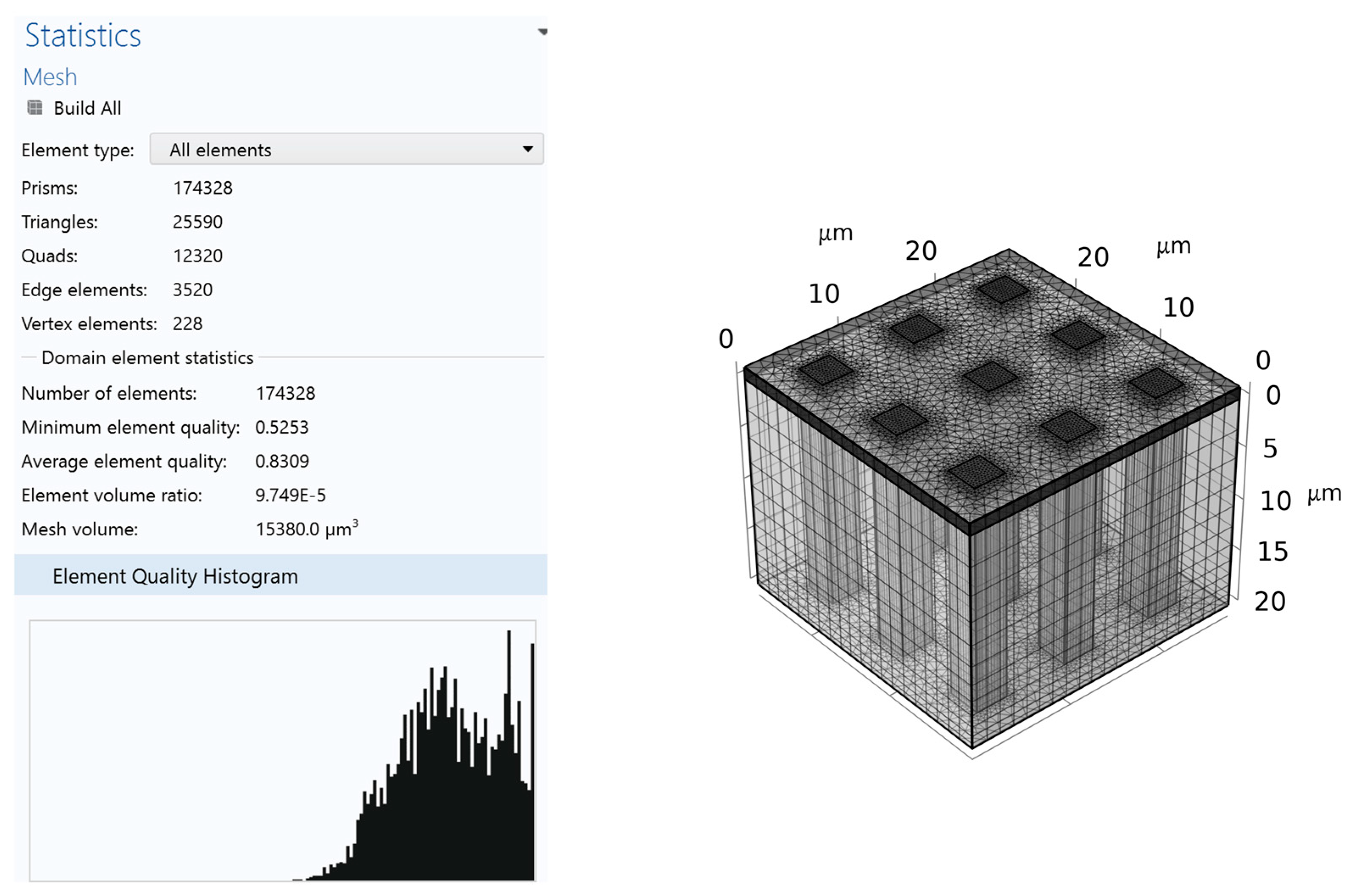
After constructing the geometric model, mesh discretization is required to partition the continuous domain into finite elements. Precise and rational meshing is critical to ensure solution convergence and accelerate convergence rates. Due to significant thermal gradients and non-uniform heating during laser irradiation, a uniform mesh distribution was inadequate. A hybrid meshing strategy was therefore implemented; a free triangular mesh with local refinement was applied at material interfaces, while swept meshing discretized bulk regions. This generated 174,328 elements collectively. The maximum element size was 2.0 μm, and the minimum element size was 0.038 μm. The final mesh configuration is illustrated in Figure 2.
When a nanosecond pulsed laser irradiates the CCD, the laser beam passes through the silicon dioxide layer in the light sensor region due to its low absorption coefficient. The laser energy then reaches the photosensitive surface of the silicon substrate directly, as silicon absorbs laser energy volumetrically [24]. The laser energy deposition function is defined as follows:
Q s i , l a s e r = α ( 1 R ) e ( α · z ) f ( t ) 2 E 0 π ω 0 2 τ e ( 2 · ( x 2 + y 2 ) ω 0 2 ) ,
where x, y, and z denote coordinate axes, t represents time, ω 0 is the spot radius, α is the absorption coefficient of the silicon for the laser, R is the reflectivity of the silicon substrate, and E 0 is the single pulse energy and τ is the pulse width.
The temporal distribution function of the laser beam can be expressed as follows:
f ( t ) = 1   ,   t τ 0   ,   τ t
Considering the CCD’s fill factor, it is crucial to note the presence of laser light shining on the light-shielded area. The laser directly heats the surface of the aluminum shielding layer. The thickness of the aluminum layer is much greater than its laser absorption depth [19], so it is treated as a surface heat source in the model. The laser energy deposition function is as follows:
Q A l , l a s e r = β f ( t ) 2 E 0 π ω 0 2 τ e ( 2 · ( x 2 + y 2 ) ω 0 2 )
where β is the absorption of the aluminum for the laser.
The temperature field on the CCD due to laser energy is governed by the differential equation of heat conduction, assuming uniform distribution and isotropy in each layer. The temperature field control equation can be expressed using Fourier’s law of thermal conduction.
ρ c T t = k 2 T x 2 + 2 T y 2 + 2 T z 2 + Q l a s e r
where Q l a s e r is the laser heat source, and ρ , c, and k are the material density, specific heat, and heat conductivity, respectively.
Accounting for surface heat dissipation via radiation and convection, the boundary condition is governed by the following:
k T n = h ( T a m b T w ) ε σ ( T a m b 4 T w 4 )
where Tw is the detector surface temperature, Tamb is the ambient temperature, h is the convective heat transfer coefficient, ε is the surface emissivity, and σ represents the Stefan’s constant. The initial temperature setting of the model is 298 K.
The temperature field is discretized spatially using quadratic serendipity elements and temporally with the Backward Differentiation Formula (BDF) scheme. These specific operational settings for numerical methods can be completed in COMSOL software.

3. Results and Discussion

3.1. Validation of the Model

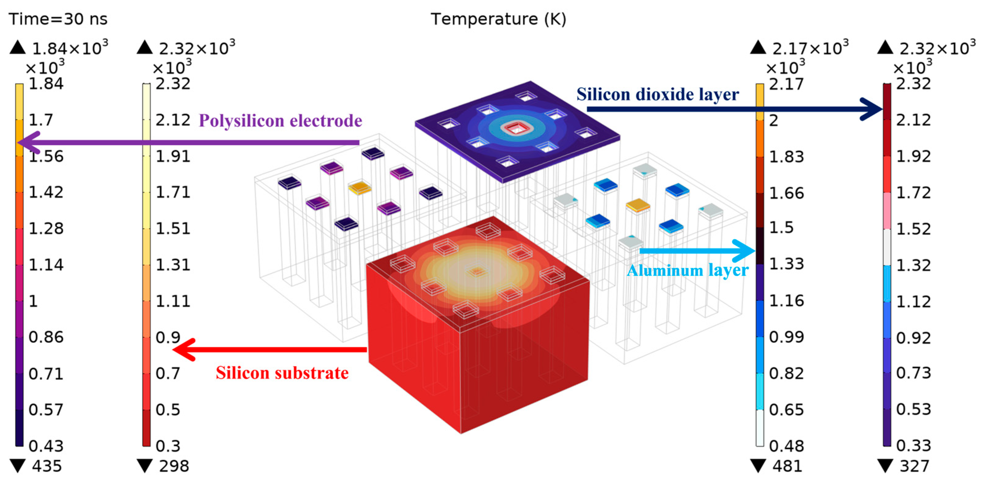
The simulation employed a Gaussian beam with a spot radius of 13 μm, a pulse width of 30 ns, and a single-pulse fluence of 1.065 J/cm2. As shown in Figure 3, upon irradiation completion (t = 30 ns), a high-temperature region formed on the silicon substrate surface, with a temperature exceeding 1685 K. Temperatures in the central area of the aluminum shielding layer rose above 2000 K but dropped below 1160 K at the edges. Among all layers, the polysilicon electrode had the lowest peak temperatures, with a maximum temperature difference of 1405 K between the central and edge regions, attributed to the thermal resistance of the silicon dioxide layer.
The temperature field evolution showed two distinct phases across all layers: rapid heating and slow cooling (Figure 4a). The aluminum shielding layer and silicon substrate reached their maximum temperatures at irradiation termination (t = 30 ns) due to laser energy absorption. The polysilicon electrode’s temperature rise depended on heat conduction, causing a 5 ns delay in reaching its peak temperature after the pulse ended. Figure 4b magnifies the heating phase from Figure 4a. The aluminum shielding layer melted at t = 6.9 ns, leading to degraded light-blocking capability and disrupting detector signal output. The silicon substrate melted at t = 19.1 ns, impairing the CCD’s photoelectric conversion function. By t = 27.2 ns, the polysilicon electrode reached its melting point (1685 K), causing internal circuit shorting and disrupting detector operation.
In the light sensor region, the laser heat source in the silicon substrate was defined as a volumetric heat source, creating significant localized temperature gradients. As shown in Figure 5a,b, at the irradiation termination time (t = 30 ns), the silicon material within a radius of 6.382 μm on the upper surface of the silicon substrate was molten. In the light-shielded region, the heat in the polysilicon electrode and silicon substrate was primarily due to thermal diffusion through lateral conduction from the irradiated silicon substrate and vertical conduction from the aluminum shielding layer. The surrounding silicon dioxide layer restricted heat diffusion, leading to local heat accumulation at the insulation layer interface. In the light-shielded region, heat diffusion from the light-shielded region caused the temperature at the four corners of the substrate surface and under the corresponding electrodes to exceed the melting point of silicon. Heat diffusion from the aluminum layer resulted in thermal damage in about 48% of the area on the electrode surface.
To quantitatively validate the model, the predicted laser fluence threshold for functional failure was compared with experimental results from Shao et al. [25]. As shown in Figure 5 and Figure 6 our simulation predicted the onset of functional failure (characterized by polysilicon electrode melting and significant substrate damage) at a laser fluence of 1.065 J/cm2 under 30 ns pulse irradiation. This result is in excellent agreement with the experimentally observed functional failure threshold of 1.146 J/cm2 reported by Shao et al. for a visible light CCD irradiated by a 532 nm laser with 8 ns pulse width [25]. The difference between the simulated and experimental thresholds is merely 7.07%, demonstrating the high accuracy of the model in predicting the critical energy density required for CCD damage. Furthermore, the simulated spatial pattern of damage involving the polysilicon electrode and substrate within the light-shielded region (Figure 5c,d and Figure 6) aligns with the established physical mechanism of thermal damage effects commonly observed in laser-induced damage experiments [13,20].

3.2. Influence of Laser Fluence on Thermal Damage
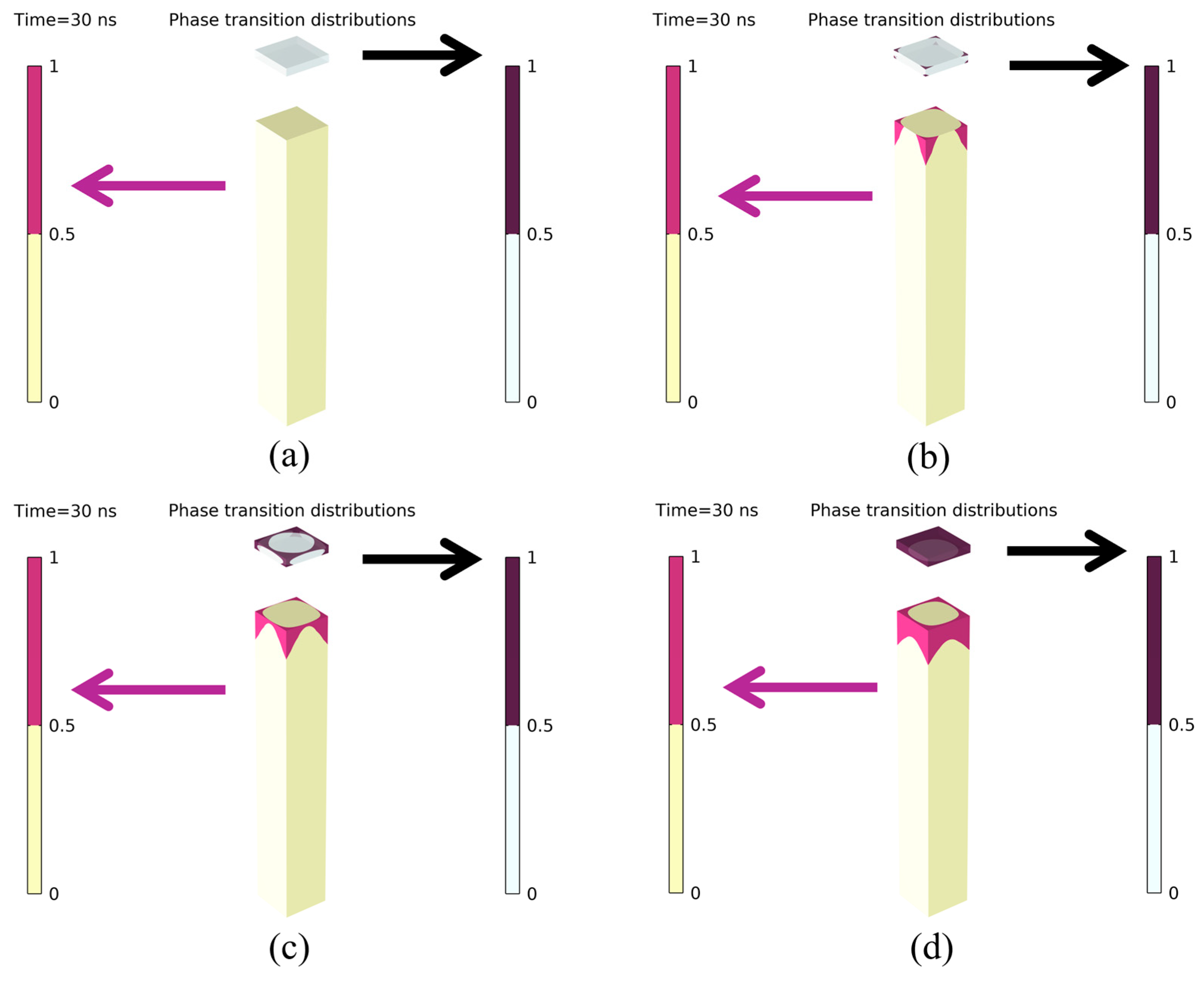
The single-pulse laser fluence values were 0.751 J/cm2, 0.987 J/cm2, 1.065 J/cm2, and 1.184 J/cm2, respectively. The temperature field distribution across the central cross-section of the CCD is shown in Figure 7, and the phase transition distribution of the polysilicon electrode and silicon substrate in the light-shielded region is depicted in Figure 6.
Figure 6. Phase transition distribution of the polysilicon electrode and silicon substrate in the light-shielded region (the laser fluence is (a) 0.751 J/cm2, (b) 0.987 J/cm2, (c) 1.065 J/cm2, and (d) 1.184 J/cm2, respectively; 0 and 1 in the phase transition images denote solid phase and liquid phase, respectively).
Aerospace 12 00791 g006
At a laser fluence of 0.751 J/cm2, the aluminum shielding layer and the photosensitive silicon substrate were damaged by direct laser irradiation, causing melting. The silicon dioxide layer and aluminum shielding layer provided protection, preventing thermal damage to the polysilicon electrode and silicon substrate in the light-shielded area. However, as the laser fluence increased, the overall temperature of the CCD increased, leading to more thermal damage. In the light sensor region, the molten size in the silicon substrate expanded more in the transverse direction than in the longitudinal direction. For example, at a laser fluence of 1.184 J/cm2, the maximum transverse molten size in the silicon substrate was 5.355 μm, while the longitudinal molten size was about 2.766 μm. In the light-shielded area, the melting of the polysilicon electrode and silicon substrate spread from the edges toward the center as the laser fluence increased. The upper surface of the electrode suffered more thermal damage than the lower surface due to additional heat accumulation from the thermal diffusion of the aluminum layer.
The results of our simulation show that there is greater transverse thermal damage in the light sensor region of silicon compared to longitudinal damage, which is consistent with findings by Kou et al. [20]. However, our study included some model enhancements, considering the absorption of laser heat by the aluminum shielding layer, and accounting for structural differences between the light sensor region and the light-shielded region. These improvements changed the pathways of heat conduction, resulting in damage progressing from the edge to the center in the light-shielded region.
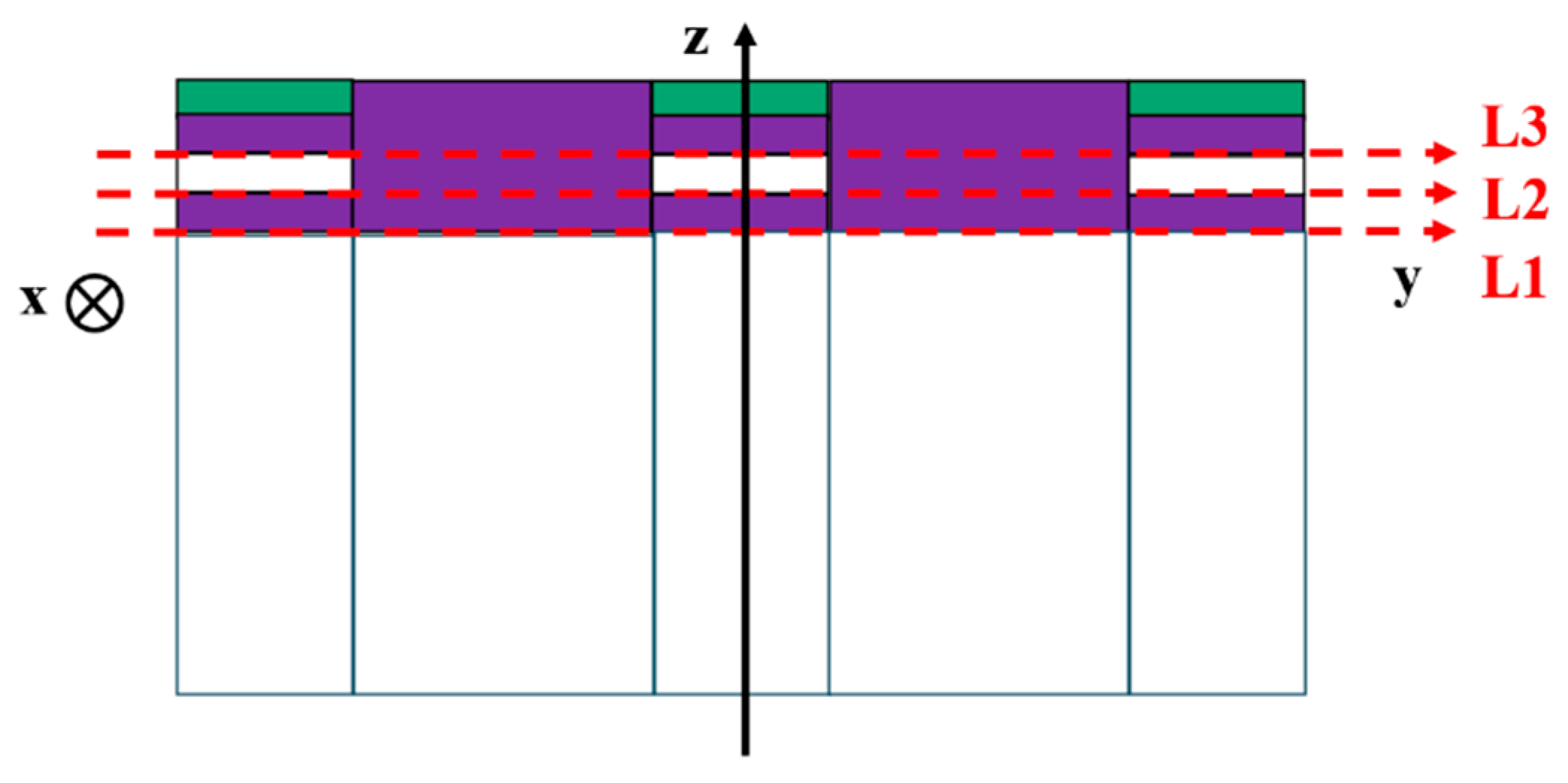
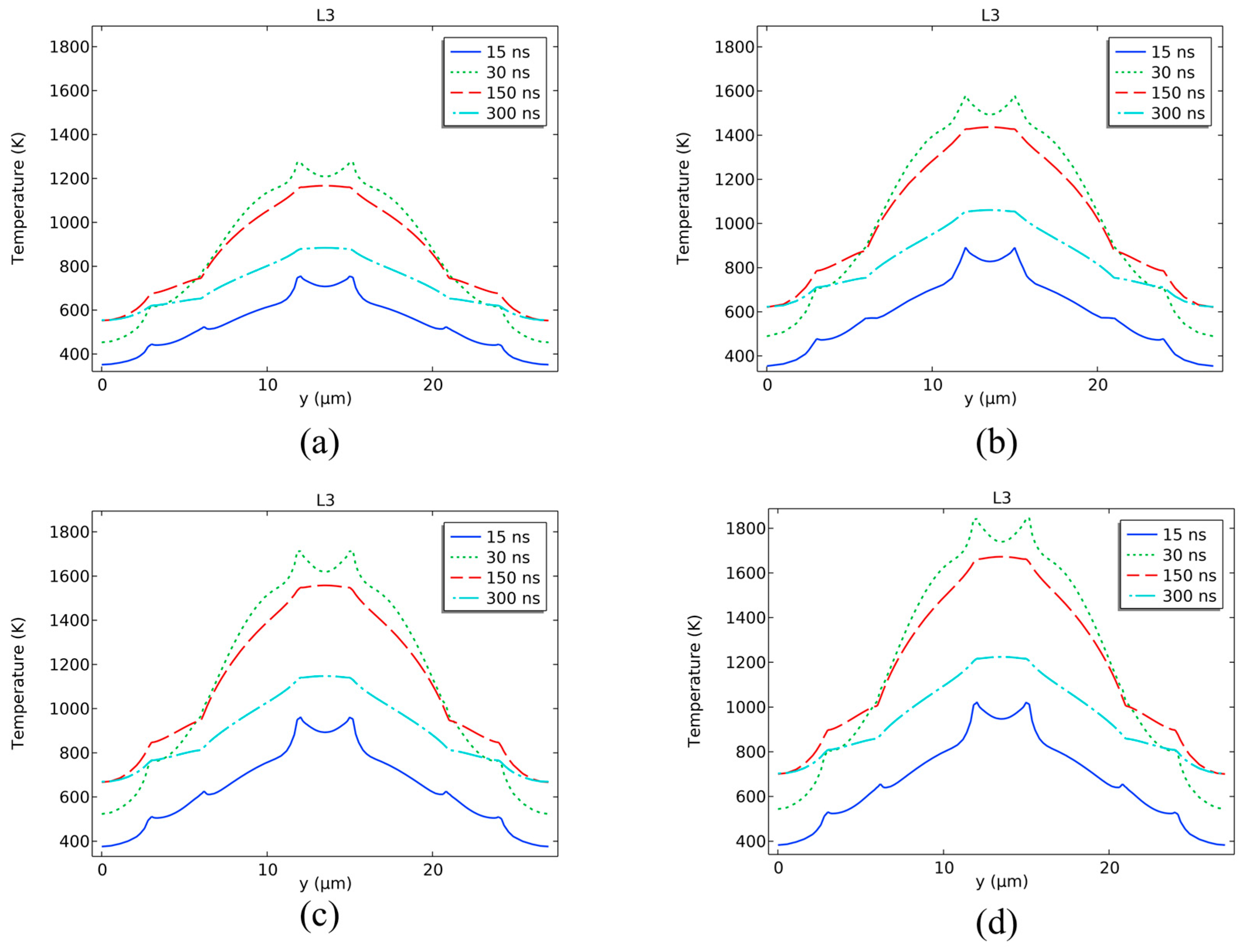
As shown in Figure 8, three special lines were set along critical interfaces of the multilayer structure to analyze the impact of laser fluence on the temperature field of the CCD. L1 was at the interface between the upper surface of the silicon substrate and the silicon dioxide layer. L2 was at the interface between the lower surface of the polysilicon electrode and the silicon dioxide layer. L3 was at the interface between the upper surface of the polysilicon electrode and the silicon dioxide layer. Temperature distributions were analyzed at four typical irradiation time points: t1 = 15 ns, t2 = 30 ns, t3 = 150 ns, and t4 = 300 ns.
As shown in Figure 9, during laser exposure (t ≤ 30 ns), localized hot zones were observed in the silicon substrate of the light sensor region (y = 0–3 μm, 6–12 μm, 15–21 μm, 24–27 μm) due to direct absorption of laser energy. In contrast, the silicon substrate in the light-shielded region did not directly absorb laser heat but rather experienced a temperature increase through thermal diffusion from the light sensor region. This resulted in a sharp temperature jump near the boundary between the two regions, creating a wavelike temperature profile with a twin-peak symmetric structure centered on the irradiation axis (y = 13.5 μm). With increasing laser fluence, the maximum temperature difference between the edges of the light-shielded region (y = 12 μm, y = 15 μm) and its center (y = 13.5 μm) increased from 347 K to 548 K. The edges of the light-shielded region melted first and gradually spread towards the center. During the cooling phase (30 ns < t ≤ 300 ns), more heat from the aluminum layer and photosensitive silicon substrate diffused into the light-shielded region, causing the isolated hot zones to merge and form a single-peak, centrally symmetric temperature distribution.
The heat received by the L2 region primarily came from thermal conduction in the photosensitive silicon substrate. As shown in Figure 10, the temperature distribution in L2 showed a wavelike pattern similar to L1 during laser exposure (t ≤ 30 ns), but due to the thermal insulation effect of the silicon dioxide layer, the temperature values in L2 were about 100 K lower than in L1. During the cooling phase (30 ns < t ≤ 300 ns), the temperature field shifted from a wavelike distribution to a single-peak pattern with higher temperatures at the center and lower values at the edges.
L3 was closer to the aluminum shielding layer compared to L2 and L1, resulting in higher temperatures in the polysilicon electrode beneath the aluminum during heating. As shown in Figure 11, the temperature distribution in the polysilicon electrode showed a saddle-shaped pattern during laser exposure (t ≤ 30 ns), with the edges (y = 12 μm, 15 μm) being hotter than the central region (y = 13.5 μm). This was due to lateral heat diffusion from the silicon substrate accumulating at the edges of the electrode. With increasing laser fluence, melting damage started at the edges and spread towards the center. During the cooling phase (30 ns < t ≤ 300 ns), the temperature distribution at L3 exhibits changes similar to those at L1 and L2, forming a unimodal, centrally symmetric temperature profile centered at y = 13.5 μm, with the peak temperature gradually decreasing.

4. Conclusions

The thermal damage of a CCD detector irradiated by the nanosecond pulsed laser was analyzed using finite element method simulations. The magnitude of temperature elevation in the CCD was primarily influenced by the laser fluence, with higher fluence resulting in a larger thermal damage area. The expansion of the molten zone within the silicon substrate in the light sensor region increased with higher laser fluence, with transverse expansion being more significant than longitudinal expansion. Damage in the light-shielded region extended from peripheral areas towards central areas with increasing laser fluence due to different energy deposition patterns and structural differences between the light sensor region and the light-shielded region.

Author Contributions

Conceptualization, H.C. and W.Z.; methodology, H.C.; software, Z.J.; validation, W.Z.; formal analysis, W.Z.; investigation, W.Z.; resources, H.C. and W.Z.; data curation, W.Z., Z.J., Y.M., X.Q. and Z.W.; writing—original draft preparation, W.Z. and H.C.; writing—review and editing, H.C.; visualization, Z.J.; funding acquisition, H.C. and W.Z. All authors have read and agreed to the published version of the manuscript.

Funding

This research was funded by the National Natural Science Foundation of China under Grant 11602304 and Grant 11502301.

Institutional Review Board Statement

Not applicable.

Informed Consent Statement

Not applicable.

Data Availability Statement

The data presented in this study are available on request from the corresponding author. Informed consent was obtained from all subjects involved in the study.

Acknowledgments

The authors would like to acknowledge Z.J. and X.Q. for their assistance with the model.

Conflicts of Interest

The authors declare no conflicts of interest.

References

  1. Towaranonte, B.; Gao, Y. Application of Charge-Coupled Device (CCD) Cameras in Electrochemiluminescence: A Minireview. Anal. Lett. 2022, 55, 186–202. [Google Scholar] [CrossRef]
  2. Wang, H.; Zhang, H.; Wang, J.; Feng, Q.; Guo, Y.-F.; Zhang, J.; Wang, Z.-Y.; Geng, Z.; Gao, J.; Liu, H.; et al. Development and performance test of a scientific CCD camera prototype for the Earth 2.0 mission. J. Astron. Telesc. Instrum. Syst. 2024, 10, 016002. [Google Scholar] [CrossRef]
  3. Wang, Z.; Ma, R.; Zeng, C.; Liu, L.; Li, X.; Wang, X.; He, B.; Ehret, G.; Chen, B.; Han, S. A fast and precise autofocus method using linear array CCD. In Optical Metrology and Inspection for Industrial Applications XI; SPIE: Cergy, France, 2024; Volume 13241. [Google Scholar]
  4. Baranov, M. Image Processing of Biological Liquids Films for Medical Diagnostics. J. Electron. Sci. Technol. 2020, 18, 100027. [Google Scholar] [CrossRef]
  5. Jamaludin, J.; Rahim, R.A.; Rahim, H.A.; Rahiman, H.F.; Muji, S.Z.M.; Fadzil, N.S.M.; Ling, L.P.; Jumaah, F.; Ahmad, A.; Ayob, N.M.N.; et al. Introducing an application of a charged coupled device (CCD) in an optical tomography system. J. Teknol. (Sci. Eng.) 2015, 73. [Google Scholar] [CrossRef][Green Version]
  6. Yu, Y.; Zhao, X.-F.; Luo, H.; Mao, Y.-D.; Tang, Z.-H. Application of CCD drift-scan photoelectric technique on monitoring GEO satellites. Adv. Space Res. 2018, 61, 2320–2327. [Google Scholar] [CrossRef]
  7. Mori, S.; Enokuchi, A.; Konoue, K. Time delay integration using COTS IT-CCD for remote sensing and other applications. In Sensors and Systems for Space Applications XIII; SPIE: Cergy, France, 2020; Volume 11422. [Google Scholar][Green Version]
  8. Schwarz, B.; Ritt, G.; Koerber, M.; Eberle, B. Laser-induced damage threshold of camera sensors and micro-optoelectromechanical systems. Opt. Eng. 2017, 56, 034108. [Google Scholar]
  9. Schwarz, B.; Ritt, G.; Koerber, M.; Eberle, B. Impact of threshold assessment methods in laser-induced damage measurements using the examples of CCD, CMOS, and DMD. Appl. Opt. 2021, 60, F39–F49. [Google Scholar] [CrossRef] [PubMed]
  10. Han, M.; Nie, J.S.; Sun, K.; Wang, X.; Dou, X.A. Experiment on the temporal evolution characteristics of a CCD multilayer structure irradiated by a 1.06-µm continuous laser. Appl. Opt. 2018, 57, 4415–4420. [Google Scholar] [CrossRef] [PubMed]
  11. Zhang, Y.N.; Niu, C.H.; Zhao, S.; Lv, Y. Investigation of interference on photodetector CCD by lasers with different wavelengths. Optik 2020, 202, 9. [Google Scholar] [CrossRef]
  12. Cheng, X.Z.; Shao, M.; Qu, W.D.; Shao, J.F.; LI, W.Z.; Fan, Y. Research on high-power laser damage to CCD detectors. Laser Infrared 2023, 53, 1743–1749. [Google Scholar]
  13. Cao, H.; Xie, X.; Chang, H.; Li, Y.; Yue, J.; Yu, Y.; Wang, G.; Tang, Z.; Li, L.; Wang, Y.; et al. Laser-induced damages to charge coupled devices with combined nanosecond/picosecond short-pulse lasers. Front. Phys. 2024, 12, 1345859. [Google Scholar] [CrossRef]
  14. Nie, J.S.; Wang, X.; Li, H.; Bian, J.T.; Hao, X.N. Thermal and mechanical damage in CCD detector induced by 1.06 μm laser. Infrared Laser Eng. 2013, 42 (Suppl. S2), 380–386. [Google Scholar]
  15. Li, G.; Shen, H.B.; Li, L.; Zhang, C.; Mao, S.J.; Wang, Y.B. Laser-induced damages to charge coupled device detector using a high-repetition-rate and high-peak-power laser. Opt. Laser Technol. 2013, 47, 221–227. [Google Scholar]
  16. Li, Z.; Wang, X.; Shen, Z.; Lu, J.; Ni, X. Mechanisms for the millisecond laser-induced functional damage to silicon charge-coupled imaging sensors. Appl. Opt. 2015, 54, 378–388. [Google Scholar] [CrossRef]
  17. Zhang, F.; Niu, Y.X.; Liu, N.; Liang, Z.J.; Liu, S. Research of temperature field and thermal stress field of CCD under laser irradiation. Laser Technol. 2017, 41, 433–437. [Google Scholar]
  18. Li, M.X.; Jin, G.Y.; Tan, Y. Simulation of the Si-CCD irradiated by millisecond pulse laser. Optik 2017, 131, 67–71. [Google Scholar]
  19. Ren, X.D.; Lei, W.H.; Wang, Y. Study on thermodynamic effect of CCD detector irradiated by laser. Optik 2019, 185, 497–504. [Google Scholar] [CrossRef]
  20. Kou, Z.; Li, Y.; Wang, G.; Li, K.; Hou, Y.; Xie, X.; Yu, Y.; Wang, Y.; Lu, Z. Temporal evolution characteristics and mechanism analysis of CCD breakdown induced by nanosecond and picosecond pulse lasers. Optik 2022, 262, 169313. [Google Scholar] [CrossRef]
  21. Cao, X.; Kang, H.; Yu, H.; Zhang, Y.; Gao, X. Liquid-solid phase transition time characteristics of CCD aluminum layer metal induced by nanosecond pulse laser. J. Appl. Opt. 2023, 44, 898–903. [Google Scholar] [CrossRef]
  22. Luštica, A. CCD and CMOS image sensors in new HD cameras. In Proceedings of the ELMAR-2011, IEEE, Zadar, Croatia, 14–16 September 2011. [Google Scholar]
  23. Peng, B. Study on the Thermal Stress of Millisecond Pulsed Laser Irradiation CCD Image Detectors. Master’s thesis, Changchun University of Science and Technology, Changchun, China, 2014. [Google Scholar]
  24. Li, Y.; Kou, Z.; Wang, G.; Hou, Y.; Xie, X.; Yu, Y.; Wang, Y.; Lu, Z. Recent advances of short-pulse laser–induced breakdown effect on charge-coupled device detectors. Opt. Laser Technol. 2022, 156, 108533. [Google Scholar] [CrossRef]
  25. Shao, J.F.; Liu, Y.; Wang, T.F.; Guo, J. Damage effect of charged coupled device with multiple-pulse picosecond laser. Acta Armament. 2014, 35, 1408–1413. [Google Scholar]
Figure 1. (a) Schematic diagram of CCD multilayer structure. (b) Three-dimensional structure of the CCD constructed in this model.
Aerospace 12 00791 g001
Figure 2. Mesh configuration of the model.
Aerospace 12 00791 g002
Figure 3. Temperature field distribution in each layer of the detector.
Aerospace 12 00791 g003
Figure 4. (a) The temperature of each layer in the CCD vs. time. (b) Magnified view of the heating phase (0–30 ns).
Aerospace 12 00791 g004
Figure 5. (a) Phase transition of the silicon substrate in the light sensor region. (b) Temperature field distribution of the silicon substrate in the light sensor region. (c) Phase transition of polysilicon electrode and silicon substrate in the light-shielded region. (d) Temperature field distribution of polysilicon electrode and silicon substrate in the light-shielded region (0 and 1 in the phase transition images (a,b) denote solid phase and liquid phase, respectively).
Aerospace 12 00791 g005
Figure 7. Temperature field distribution across the central cross-section of the CCD (the laser fluence is (a) 0.751 J/cm2, (b) 0.987 J/cm2, (c) 1.065 J/cm2, and (d) 1.184 J/cm2, respectively).
Aerospace 12 00791 g007
Figure 8. Special lines for analysis in the model.
Aerospace 12 00791 g008
Figure 9. Temperature distribution of L1 (the laser fluence is (a) 0.751 J/cm2, (b) 0.987 J/cm2, (c) 1.065 J/cm2, and (d) 1.184 J/cm2, respectively).
Aerospace 12 00791 g009
Figure 10. Temperature distribution of L2 (the laser fluence is (a) 0.751 J/cm2, (b) 0.987 J/cm2, (c) 1.065 J/cm2, and (d) 1.184 J/cm2, respectively).
Aerospace 12 00791 g010
Figure 11. Temperature distribution of L3 (the laser fluence is (a) 0.751 J/cm2, (b) 0.987 J/cm2, (c) 1.065 J/cm2, and (d) 1.184 J/cm2, respectively).
Aerospace 12 00791 g011
Table 1. The thermodynamic parameters of materials.
ParametersPIAlSiO2Si
Density/(kg/m3)1530270926402330
Thermal conductivity/(W/m·K)0.122541.327
Specific heat/(J/kg·K)109010507871009
Melting point/K71093218801685
Disclaimer/Publisher’s Note: The statements, opinions and data contained in all publications are solely those of the individual author(s) and contributor(s) and not of MDPI and/or the editor(s). MDPI and/or the editor(s) disclaim responsibility for any injury to people or property resulting from any ideas, methods, instructions or products referred to in the content.