Article

Validation of PCB Strain-Based Methodology for Structural Design of Spaceborne Electronic Equipment Under Vertical Mounting Conditions in Launch Environments

by
Jae-Cheol Hwang
1,2,
Kwang-Woo Kim
1 and
Hyun-Ung Oh
1,2,*
1
Department of Aerospace and Mechanical Engineering, Korea Aerospace University, 76 Hanggongdaehak-ro, Deogyang-gu, Goyang 10540, Gyeonggi-do, Republic of Korea
2
Department of Smart Air Mobility, Korea Aerospace University, 76 Hanggongdaehak-ro, Deogyang-gu, Goyang 10540, Gyeonggi-do, Republic of Korea
*
Author to whom correspondence should be addressed.
Aerospace 2025, 12(9), 770; https://doi.org/10.3390/aerospace12090770
Submission received: 10 June 2025 / Revised: 24 August 2025 / Accepted: 25 August 2025 / Published: 27 August 2025
(This article belongs to the Section Astronautics & Space Science)

Abstract

Spaceborne electronic equipment printed circuit boards (PCBs) installed under vertical mounting boundary conditions are exposed to a tougher environment than horizontal mounting due to the boundary conditions under the launch environment. Steinberg’s theory, which was previously applied to evaluate the structural safety of spaceborne electronic equipment, generates large errors and leads to inaccurate results. Although the vertical mounting of spaceborne electronic equipment is increasing due to its thermal/structural advantages, no high-reliability methodology or research has been developed to secure structural safety in the launch environment. In this study, the Oh-Park methodology, a highly reliable technique for evaluating the structural safety of solder joints in space-use electrical components based on the strain of the PCB, was verified for vertical spaceborne electronic equipment. Consequently, fatigue life tests were performed on specimens with structures similar to those of the actual spaceborne electronic equipment. The results were compared and analyzed with predictions made using Steinberg’s theory and Oh-Park methodology, respectively. The structural safety assessment using the Oh-Park methodology represented the test results more accurately, indicating that the critical strain-based methodology is effective for the design of vertical spaceborne electronic equipment exhibiting more complex behaviors due to their structural characteristics.

1. Introduction

Spaceborne electronic equipment provides essential functions for operating satellite systems during on-orbit missions. With the ongoing development of small satellites, a growing demand for higher-performance spaceborne electronic equipment has emerged, which constitutes a significant portion of mission-critical systems. Concurrently, recent trends in satellite electronic systems have increasingly emphasized miniaturization and weight reduction as essential approaches for lowering development and launch costs. Kim and Hwang [1] evaluated the random vibration reliability of PBGA electronic packages under space conditions, highlighting the need for compact, high-performance, and reliable components for small satellite platforms. Jang et al. [2] proposed a modular housing design using composite materials, achieving a significant reduction in mass compared to conventional metallic housings, thereby demonstrating that lightweight design can directly contribute to reducing satellite development costs. Krumweide and Tremblay [3] discussed the mechanical and thermal limitations associated with the application of composite materials in electronic packaging, underscoring the challenges that must be addressed to ensure the reliability of lightweight structures. Fenske et al. [4] presented a lightweight housing that achieved up to 69% mass reduction and explicitly demonstrated that such reductions directly translate into lower development and launch costs. Similarly, Aglietti [5] introduced lighter housings for spaceborne electronic equipment, achieving approximately 20% mass reduction while maintaining mechanical and thermal safety, thereby demonstrating that lightweight design can be realized without compromising reliability.
Highly integrated electronic packages are being deployed to satisfy the increasingly demanding requirements of satellites. However, these packages are highly susceptible to solder joint fatigue in extreme random vibration environments during launch. Repetitive bending motions caused by random vibrations are a leading factor in the initiation of fatigue failures in solder joints, which serve as both electrical and mechanical connections between electronic packages and printed circuit boards (PCBs) [6,7,8]. The failure of these solder joints can generate electrical malfunctions or even mission failure; therefore, the structural safety of solder joints is crucial for the success of satellite missions. As a result, high-reliability structural design techniques are essential [9,10].
Steinberg’s fatigue failure theory, proposed in the 1970s, is the most widely applied approach for the structural design of spaceborne electronic equipment [11]. This theory predicts the allowable displacement of solder joints in PCBs and single electronic packages that are exposed to random vibrations. When internal PCB bending occurs due to external disturbances, a fatigue life of approximately 20 million cycles in a random vibration environment can be achieved if the maximum displacement is kept below the allowable limit. A study demonstrated that the board displacement can be reasonably estimated even when the finite element model of the electronic package, including the solder joint, is simplified with a beam or rigid link elements [12].
Several recent studies have highlighted the limitations of Steinberg’s theory [13,14,15,16]. One significant limitation is the relative positioning factor in Steinberg’s formula, which determines the location of an electronic package on a PCB. This factor tends to overestimate the margin of safety (MoS) as the mounting area of the electronic package approaches the corners of the PCB. In addition, the 20-million-cycle fatigue life standard proposed by Steinberg is often excessively conservative for spaceborne electronic equipment because the actual accumulated fatigue during vibration testing and launch is much lower [13]. Because Steinberg’s empirical formula assumes that the PCB has a half-sine mode shape, this formula does not consider the complex mode shapes caused by asymmetrical PCB geometries, irregular fastening-point locations, and reinforcement. These discrepancies result in errors in the calculated allowable displacement, compromising the reliability of the results of the structural safety evaluations of solder joints.
To address these limitations, Park et al. [17] proposed a critical strain-based structural design methodology (Oh-Park methodology). This approach evaluates the structural safety of joints under random vibrations based on MoS calculations derived from the PCB strain. Unlike Steinberg’s theory, which applies a fixed design criterion of 20 million cycles, the Oh-Park methodology calculates MoS based on the fatigue cycles accumulated from the ground test phase through to the actual launch of the spaceborne electronic equipment. The Oh-Park methodology prevents excessive MoS derived from Steinberg’s fixed cycle standard by using the design factor ( D F ) based on the required time to failure ( T T F r e q ). This D F reflects the accumulated fatigue in the solder joints during both the vibration test and launch phases. This method overcomes Steinberg’s theory by calculating MoS for the critical and in-plane maximum principal strains of the PCB’s derived from a finite element analysis (FEA). In addition, the methodology includes a simplified finite element modeling technique that enables faster model construction than detailed modeling, which is time-consuming for PCBs and electronic packages.
Previous studies have focused on the structural validation of spaceborne electronic equipment, primarily on configurations mounted horizontally to the ground [18,19,20]. However, vertical fastening has been increasingly used in recent spaceborne electronic equipment designs because this mounting may be advantageous in certain design situations. For example, in terms of thermal design, spaceborne electronic equipment with integrated high-heat components can provide a more effective heat dissipation path when mounted vertically. This mounting pattern can improve the thermal-management performance of the entire system. In particular, vertical mounting is considered, for spaceborne electronic equipment designed with high heat dissipation density [21]. Additionally, vertical mounting is often selected in terms of space utilization.
Recent satellite system designs require the integration of additional modules into a single panel to reduce their size and increase their performance. This is because, if spaceborne electronic equipment are arranged horizontally, heat dissipation is restricted and effective mitigation of the heat generated by high-heating components is challenging. Instead, mounting electronic equipment in a vertical direction ensures a heat conduction path between the spaceborne electronic equipment and the panel, while allowing heat to dissipate toward deep space through the outer wall of the panel. In addition to these thermal management advantages, the vertical mounting method is gradually expanding in various mission platforms, such as communication satellites, geostationary satellites, and small satellites, mainly because of advantages in limited panel areas. The proportion of system using the mounting arrangement is expected to increase in the future [22,23,24,25].
However, vertical mounting exhibits a different behavior compared to horizontal mounting in terms of the structural response, as shown in Figure 1. In a horizontal mounting configuration, the PCB is pressed against the base panel and across the front through the housing, mechanically constraining the entire structure. Under these conditions, even if an external vibration stimulus is applied, the elastic mode of the housing structure is suppressed, and the complex vibration behavior resulting from the mixing of the local mode of the PCB and the global mode of the housing is greatly limited. Because the out-of-plane bending deformation is suppressed in the direction perpendicular to the panel surface, the local deformation is reduced even under launch and dynamic load conditions. This contributes to reducing fatigue in solder joints and ensuring the structural stability of spaceborne electronic equipment [26].
Furthermore, in a vertically mounted structure, the entire system vibrates in a global mode, which may interact with the local modes of the PCB itself, resulting in complex mode mixing phenomena. This phenomenon is more prominent than that in horizontally mounted structures, and it increases structural vulnerability, especially in external vibration environments. This is due to the irregular boundary conditions appearing in the vertical mounting structure and the elastic mode effects of the housing. As shown at the bottom of Figure 1, the vertically mounted spaceborne electronic equipment vibrates in a global half-sine bending mode throughout the structure due to limited support conditions, which interacts with the elastic modes of the housing itself to induce an asymmetric and localized response. This causes the local modes of the PCB to be sensitive to housing deformation; consequently, the mode shape of the entire system is complex. In contrast, in the horizontal mounting structure (Figure 1, top), the PCB and satellite panel are in full contact with each other such that vibration energy is effectively dissipated, the intervention of the housing elastic mode is suppressed, and a symmetrical mode shape is maintained. Due to these differences, analysis approaches that assume single-mode-based local responses, such as Steinberg’s theory, do not sufficiently reflect the complex response characteristics in vertically mounted structures.
For horizontal mounting (Figure 1, top), the satellite panel acts as a structural foundation to effectively damp the vibrational energy, resulting in a symmetrical mode shape confined to the PCB itself. In this case, the out-of-plane deformation of the PCB is uniformly distributed, and the influence of the support structure is minimal. Furthermore, for vertical mounting (Figure 1, bottom), the satellite panel does not effectively damp vibration. Thus, the PCB is directly exposed to vibration loads. This results in an asymmetric and inhomogeneous deformation pattern, with the elastic mode influence of the housing structure, which is particularly noticeable in the upper region. These results suggest that vertically mounted spaceborne electronic equipment is vulnerable to dynamic coupling effects with the support structure and demonstrate that consideration of the mounting orientation is essential under dynamic conditions such as a launch environment. That is, the out-of-plane direction of the PCB matches the in-plane direction of the spaceborne electronic equipment, which has a structural limitation that prevents the satellite panel from providing a vibrational damping effect. This structural configuration causes the entire housing to act as a single support and exhibits the characteristic that the elastic mode of the housing structure of the spaceborne electronic equipment directly affects the vibrational mode of the PCB. These composite modes are not vibrations of the PCB alone, but rather a combination of global bending of the entire module and local modes of the PCB itself.
Moreover, vertically mounted spaceborne electronic equipment requires a completely different structural dynamic analysis compared to horizontally mounted spaceborne electronic equipment. However, most current evaluation theories have been developed based on horizontal mounting conditions and applying them directly to vertically mounted spaceborne electronic equipment is likely to lead to fundamental errors. In some studies, simple PCB specimens with attached single electronic packages were fabricated and tested to simulate vertical mounting conditions [27]. However, this is limited to observing the elastic mode effect of the housing structure. The tested specimens rarely reflected the complexity of real spaceborne electronic equipment, and featured a limited number of packages, simplified boundary conditions, and intentionally engineered modal responses. Therefore, there is an inherent gap that will be present between the structures of spaceborne electronic equipment in which various electronic packages are integrated in an actual space environment.
Finally, the research on vertical mounting to date has been limited to basic attempts and has clear limitations in extending the findings to structures targeting complex spaceborne electronic equipment in actual operation. In actual spaceborne electronic equipment, various types of electronic packages, such as the Plastic Ball Grid Array (PBGA), Quad-Flat Package (QFP), and Thin Small Outline Package (TSOP), are mixed and mounted, each of which has its own unique mass, stiffness, and damping characteristics. This results in the mode shapes of the entire housing and PCB system being complex and nonlinear, which cannot be realized in a single specimen. Moreover, it is difficult to evaluate structural safety in an actual space environment using a simplified test specimen. Another crucial aspect is that when multiple electronic packages are mounted on a single PCB, the failure of a solder joint on one package can change the boundary conditions at that location and affect the structural behavior of the surrounding packages. These changes in boundary conditions can affect the natural vibration characteristics and fatigue life of adjacent packages, which are difficult to predict using simplified specimens based on a single package. In a real spaceborne electronic equipment in which a comprehensive specimen is installed, each package acts as a dynamic boundary condition for the other packages. Thus, the system exhibits more complex and nonlinear mode shapes. These complex mode shapes are represented by global banding and local modes, which are important for more realistically reflecting the mechanisms of fatigue accumulation and failure occurrence inside spaceborne electronic equipment.
Therefore, vertically mounted spaceborne electronic equipment requires separate validation studies that consider their composite structures, and simple single-specimen tests or horizontally mounted-base results are insufficient. Previous studies [27] have been useful for understanding the basic characteristics of vertically mounted structures. However, reflecting the effects of structural asymmetry, interactions between multiple packages, and elastic modes of actual housing is challenging in simple specimens using a single electronic package. It is essential to verify the validity of the Oh-Park methodology by simulating real spaceborne electronic equipment with various electronic packages mounted on them and evaluating fatigue life and structural safety under vertical mounting conditions, which accurately reflect the complex and irregular deformation behavior unique to vertical mounting.
The purpose of this study is to evaluate the structural safety of vertically mounted spaceborne electronic equipment by applying the Oh-Park methodology and to verify the validity of the methodology by comparing it with the existing Steinberg’s theory. Through this, we aim to examine the practical applicability in designs that reflect various boundary conditions and structural complexity. Comprehensive PCB specimens with multiple electronic packages mounted and a housing simulating a vertically mounted structure were manufactured, and fatigue life tests were performed on them. By applying Steinberg’s theory and the Oh-Park methodology, respectively, the accuracy of life prediction and the validity of structural safety assessment of each technique were compared and analyzed.
The test results showed that Steinberg’s theory could not sufficiently reflect the local deformation and complex mode characteristics of the entire system, and the predicted life showed a large difference from the actual observed failure time. In contrast, the Oh-Park methodology was more precise in reflecting the structural behaviors occurring under various electronic package combinations and vertical mounting conditions within spaceborne electronic equipment, thereby enabling highly reliable life prediction and design verification.

2. Structural Design Methodology

Satellites are placed in very harsh environments due to noise and vibrations generated during the launch process. These forces are transmitted inside through the rocket structure, affecting both the satellite and its internal spaceborne electronic equipment [28]. Such excitation from noise and vibration has a significant impact on the PCBs and electronic packages within spaceborne equipment, where random vibrations during vibration testing and launch induce fatigue in the solder joints of electronic packages. This accumulated fatigue is the main cause of functional failure. Therefore, predicting the structural safety of electronic package solder joints during the design stage is critical for ensuring mission success.

2.1. Steinberg’s Theory

Steinberg’s theory is widely applied for evaluating the structural safety of spaceborne electronic equipment. It provides an empirical formula for estimating the allowable displacement δ a l l o w of PCBs, which is calculated as follows:
δ a l l o w = 0.0028 d C t r L   [ m m ] ,
where C is a constant related to the electronic package configuration, t is PCB thickness, r is a relative position coefficient of the electronic package on the substrate, L is the length of the electronic package, and d is the length of the electronic package parallel to the PCB. The MoS for the solder joint is then calculated based on the allowable displacement and maximum displacement using Equations (1) and (2).
M o S = δ a l l o w F o S × δ m a x 1 > 0 ,
where F o S is the Factor of Safety. This empirical formula for allowable displacement in Steinberg’s theory assumes that the PCB is rectangular, with all edges simply supported, resulting in an ideal half-sinusoidal mode shape. Consequently, in actual cases where the PCB has a complex mode shape due to its asymmetrical geometry, irregular constraint points locations, or the application of reinforcement, errors arise when calculating the allowable displacement using Equation (1). A significant source of error is the relative position coefficient r , which tends to overestimate the allowable displacement as the mounting location of the electronic package approaches the PCB edge. In addition, when the PCB mode shape becomes complex, determining accurate values for the d and r coefficients become ambiguous, leading to inaccurate predictions, such as excessive MoS compared with the actual fatigue life of solder joints.

2.2. Oh-Park Methodology

To overcome these limitations, Park et al. [17] proposed a structural design methodology based on critical strain theory (Oh-Park methodology). This method evaluates structural safety by focusing on PCB strain rather than displacement. The critical strain ε c , representing the threshold shear direction strain for electronic packages on the PCB, is calculated by modifying the d and r coefficients in Equation (1), which are the primary sources of error. The critical strain ε c is expressed as follows:
ε c = ζ C L ,
where ζ is calculated as the PCB allowable strain as in Equation (4).
ζ = 2.35 t × 1900 300 × log ε ˙ ,
ε ˙ = 2 π × ε p m a x × f n ,
where ε ˙ is the PCB strain obtained using Equation (5). In Equation (5), ε p m a x represents the maximum principal strain of the PCB derived from random vibration analysis results. ε p m a x is calculated as the 3 σ value of the principal strain under random vibration conditions, assuming a Gaussian normal distribution, as shown in Equation (6) [29].
ε p m a x = 3 × ε x r m s + ε y r m s 2 + ε x r m s ε y r m s 2 + ε x y r m s 2 ,
where ε x r m s and ε y r m s represent the root mean square (RMS) strains of the PCB in the x-axis and y-axis directions, respectively, while ε x y r m s represents the RMS strain in the PCB shear direction.
One of the primary limitations of Steinberg’s theory is that the design criterion of 20 million cycles provides an excessive margin compared to the actual fatigue cycles accumulated during vibration testing and launching of spaceborne electronic equipment. This results in structural overdesign, leading to unnecessary increases in weight and cost [13]. To overcome this issue, the Oh-Park methodology establishes a preemptive framework that aligns with the actual test and launch procedures for satellite system and spaceborne electronic equipment. This approach derives MoS by calculating T T F r e q and D F based on the actual fatigue cycles accumulated during testing and launch. The test procedure was performed by gradually increasing the vibration level and converting it into an equivalent test duration to the 0 dB standard. This conversion is crucial because the structural analysis of spaceborne electronic equipment is typically conducted at the 0 dB qualification level using random vibration inputs. When calculating the MoS based on critical strain, T T F r e q was estimated as the design life by considering the accumulated fatigue cycles until solder joint failure during the test and launch processes, as expressed in Equation (7) as follows:
T T F r e q = Σ T C Q + Σ T s / s A + Σ T L × F o S t t f ,
T C Q , T S / S A = T x d B ,
where F o S t t f is a safety factor for T T F r e q , with a value of 4, as recommended by the European Cooperation for Space Standardization (ECSS) [30]. The term Σ T C Q represents the fatigue time during component-level qualification testing, while Σ T S / S A represents the fatigue time during satellite system-level acceptance testing. The equivalent fatigue time at different excitation levels x is used to calculate these terms, as shown in Equation (9).
T x d B = ( t t e s t or   t l a u n c h ) ×   G b × N ,
G = 10 x 20 ,
where t t e s t and t l a u n c h represent the duration of the level-specific vibration test time and the actual random vibration during launch, respectively. N is the number of vibration tests per axis, and G is the ratio of the RMS input test level to the excitation level x , calculated using Equation (10). A fatigue exponent b of 6.4 was applied for the Sn-Pb solder material. Σ T L is the damage time during the actual launch stage, if an acceptance test level of −3 dB vibration occurs simultaneously along all three axes, with the device exposed to random vibration for 4 min [31]. MoS based on the critical strain was calculated using Equation (11), where D F is calculated using in Equation (12) with T T F r e q reflecting the accumulated fatigue cycles during the test and launch stage, and the design factor derived from the natural frequency.
M o S = D F × ε c ε p m a x 1 > 0 ,
D F = n o r g n r e q 1 / b = 2 × 10 7 T T F r e q × 60 × f n 1 / b ,
where n o r g represents the fatigue failure under random vibration, and n r e q represents the total fatigue life cycle required for the survival of the electronic package.
D F is a factor that relatively corrects the reference fatigue life based on the cumulative fatigue life that a solder joint must withstand under actual vibration environment. When calculating MoS, it is multiplied by the critical strain and used as the corrected allowable strain. It is then compared to the maximum principal strain to quantitatively determine fatigue life is suitability.
To verify whether the calculated MoS accurately reflects the electronic package T T F obtained from the test results, T T F was estimated using both Steinberg’s theory and the Oh–Park methodology for comparison. The predicted T T F p r e d using Steinberg’s theory based on PCB displacement is as follows:
T T F p r e d = N c × ( Z a l l o w Z m a x ) b × ( 1 f n × 60 ) ,   [ min ]
The T T F p r e d predicted by Oh-Park methodology based on PCB strain is as follows:
T T F p r e d = N c × ( ε c ε p m a x ) b × ( 1 f n × 60 ) ,   [ min ]
where N c is 2 × 10 7 , which is the number of random vibration cycles.
This methodology was validated under vertical mounting conditions in a previous study using a single-mounted electronic package [27]. Under these simple conditions, the mode response appears as a relatively standardized shape, but in the case of actual spaceborne electronic equipment, various shapes and numerous electronic packages are mixed and mounted on the PCB, so the entire structure exhibits a complex mode shape. These composite modes cause a nonlinear response, which affects the fatigue life of each solder joint. Therefore, in this study, to verify the validity of the Oh-Park methodology under conditions that actually reflect such complex structures, comprehensive PCB specimens and housing modules consisting of various electronic packages with different boundary conditions were fabricated, and the validity of the methodology was verified under vertical conditions in terms of actual design through fatigue life tests.

3. Fatigue Life Test of Electronic Equipment Module

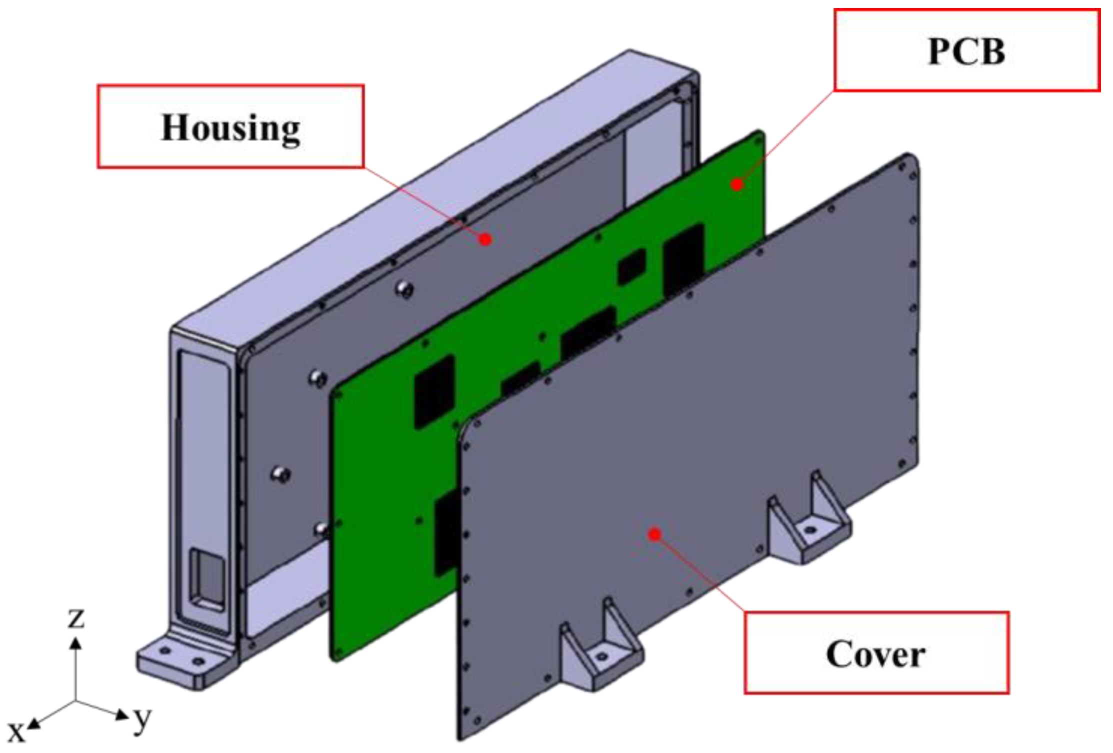
To validate the Oh-Park methodology for vertically mounted spaceborne electronic equipment, a comprehensive PCB specimen and housing module with various electronic packages were designed and manufactured, as shown in Figure 2.

3.1. Description of Electronic Equipment Module

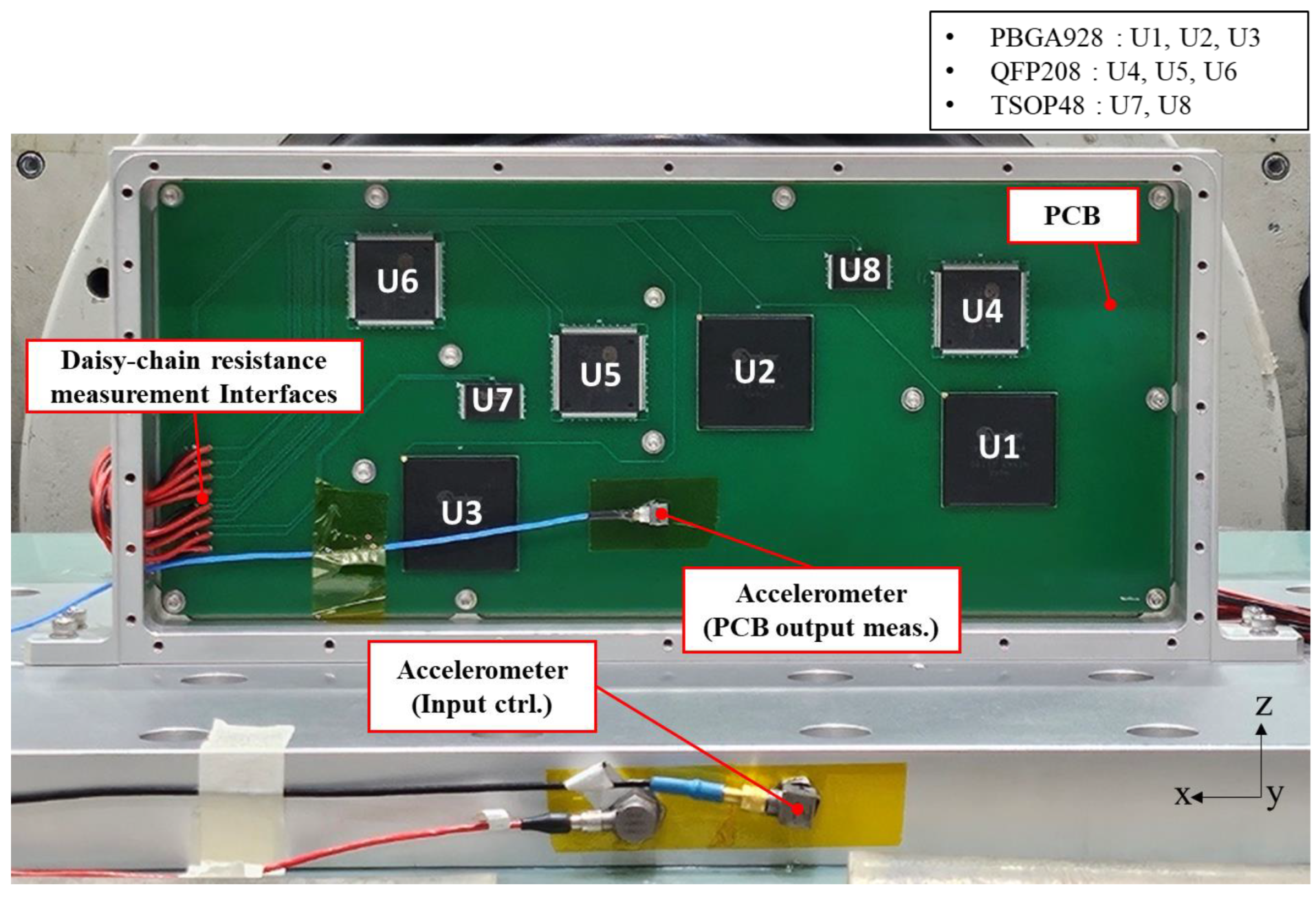
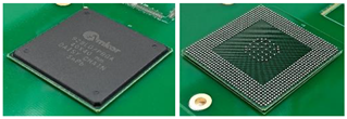
For the comprehensive PCB specimen, the electronic packages and fastening-points were intentionally placed at irregular locations to create various boundary conditions. The PCB was manufactured using FR-4 laminate with an area of 150 × 350 mm and a thickness of 1.6 mm. Eight electronic packages, including three PBGA928, three QFP208, and two TSOP48 packages, were mounted on the specimen. These three types of packages were selected due to their relatively high probability of failure among those commonly used in spaceborne electronics. Dummy packages with electrical functionality were used instead of standard packages with specifications identical to those listed in Table 1.
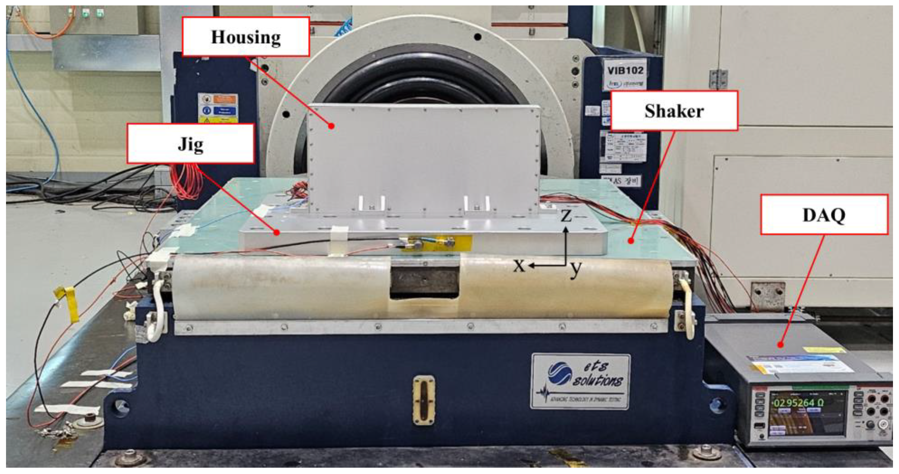
A dummy package fabricated with a daisy-chain circuit, in which all solder joint pins are connected in series, was used to detect cracks in the solder joints by monitoring changes in circuit resistance. The comprehensive PCB specimen was mounted on a housing module made of Al-6061 T6. The housing module measured 370 × 206 × 30 mm and weighed approximately 2.0 kg. Figure 3 and Figure 4 show the fatigue-life test setup for the comprehensive PCB specimen and a housing module mounted on a vibration exciter, respectively.

3.2. Random Vibration Fatigue Life Test

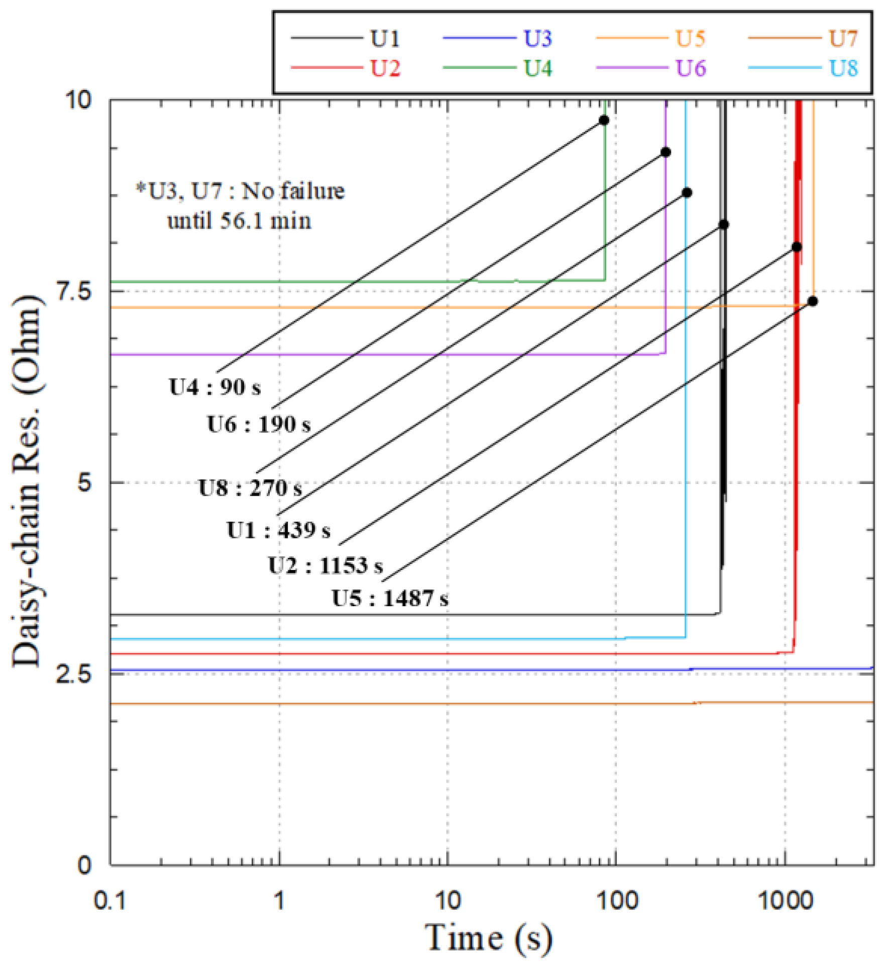
The fatigue life test was performed with excitation along the y-axis of 20 G r m s . Table 2 lists the acceleration spectral density (ASD) conditions used in the tests, including ASD values for each frequency range and overall amplitude level. These conditions were used as typical input conditions in both the Steinberg’s theory and the Oh-Park methodology. Although the actual launch vibration environment is typically at the level of 12–14 G r m s , a higher level was intentionally applied in this test to induce specimen failure and measure the time to failure. The test continued until the solder joint failure criterion was satisfied. A data acquisition device (DAQ6510. Keithley Co. Ltd., Cleveland, OH, USA) was used to measure the two-wire resistance of each electronic package to determine failure occurrence. The DAQ had a measurement accuracy of less than 10 2 Ω and a sampling rate of 1.7 samples per second. Based on the IPC-9701A standard, a solder joint failure was defined as a daisy-chain resistance exceeding 20% of the initial value for more than five consecutive measurements during the test [32].
Figure 5 and Figure 6 show the daisy chain resistance over time for each sample, with the corresponding values listed in Table 3. Samples 1 and 2 were manufactured using the same configuration and processes. Samples 1 and 2 in this study considered specimens with identical structures, each with the same electronic package, vertical mounting structure, housing module, and fixing conditions. However, to ensure experimental repeatability, fatigue life tests were conducted using two specimens, and the reliability of the methodology was assessed by comparing the results. The failure sequence of the electronic packages was U4 → U6 → U8 → U1 → U2 → U5, with failure generally occurring in the order of increasing distance from the mounting surface. Although packages U3 and U7 survived the testing despite negative MoS predictions, this result is attributable to boundary-sensitive nonlinear effects, such as local stiffener interactions, fastening-point proximity, and load redistribution. These discrepancies highlight the inherent challenge of fatigue-life prediction in vertical configurations, where uncertainty is amplified. In addition, the results confirm that the Oh–Park methodology provides higher overall reliability with reduced arbitrariness compared to Steinberg’s theory [33,34]. These test results were used to validate the Oh-Park methodology for comprehensive PCB specimen-level spaceborne electronic equipment with multiple vertically mounted electronic packages.

4. Verification of the Structural Design Methodology

The Oh-Park methodology was verified for vertically mounted spaceborne electronic equipment by constructing a finite element model. Subsequently, structural analysis was performed based on the simplified finite element modeling technique proposed by Park et al. [17].

4.1. Structural Analysis Modeling

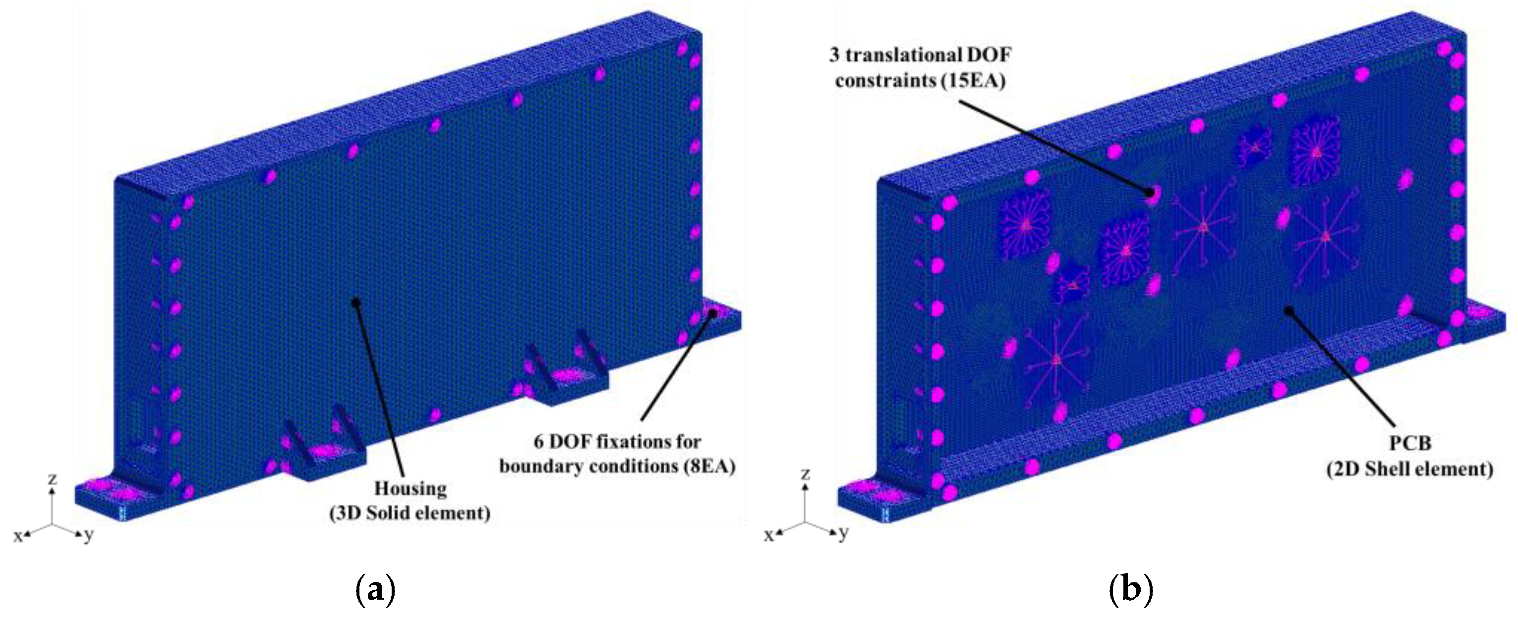
The structural safety of various electronic packages was evaluated based on fatigue-life test results, and a comparative analysis between the Oh-Park methodology and Steinberg’s theory was performed. Figure 7 shows the electronic package and finite element modeling configuration for the housing module and the comprehensive PCB specimen. Table 4 summarizes the material properties used in the finite element analysis of the PCB and housing structures. The elastic modulus, Poisson’s ratio, and density were defined for FR-4 for the PCB substrate and A6061-T6 aluminum for the housing module, and the properties were applied consistently throughout all structural analysis steps. The housing module was modeled using tet10 3D solid elements, and six degrees-of-freedom (DOF) constraints were applied at the eight bottom surface fastening-points.
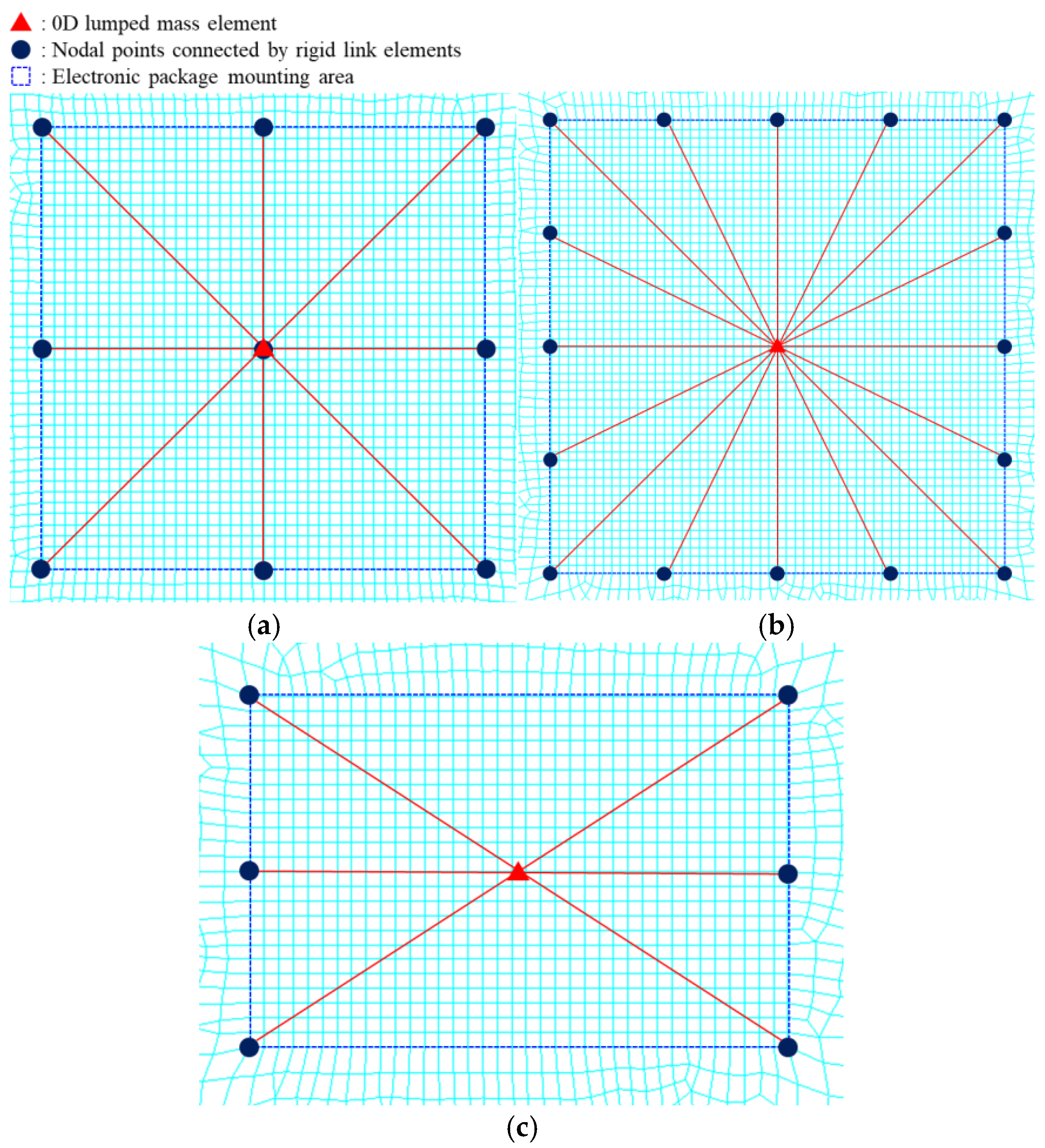
The following is a simplified modeling technique for PBGA928, QFP208, and TSOP48. The PCB was modeled using QUAD4 and Tria3 2D shell elements. For flat structures such as PCBs, shell elements offer less deformation than solid elements, reducing mesh density and leading to more accurate strain estimates. In contrast, solid elements can overestimate stiffness, leading to inaccurate staining results. Additionally, determining an appropriate shell size is essential to avoid overestimation of strain. The specimen strain may be exaggerated when the elements are constrained by rigid rinks [17]. To address this, Park et al. [17] developed a mesh modeling method that enables reasonable strain estimation, which was applied in this study. The PCB area occupied by an electronic package was uniformly meshed with a size equal to the body length of the package divided by the number of solders balls or leads on one side. The remaining PCB area was meshed with a mesh of 1.5 mm size. Bolt joints between the electronic package and PCB were subjected to three degrees of freedom (DoF) constraints. The electronic packages were modeled as 0D lumped masses, concentrating the mass of each device at a single point, as suggested in previous studies [17,35,36]. This simplified finite element modeling technique significantly reduces the time required to develop the model while maintaining accuracy. Based on repeated structural safety evaluations of various electronic packages in previous studies, appropriate node modeling was applied to each package. Figure 8 illustrates the node configuration: (a) PBGA 928 with nine nodes, (b) QFP208 with 16 nodes, and (c) TSOP48 with six nodes, each modeled in the same area as the corresponding electronic package size.
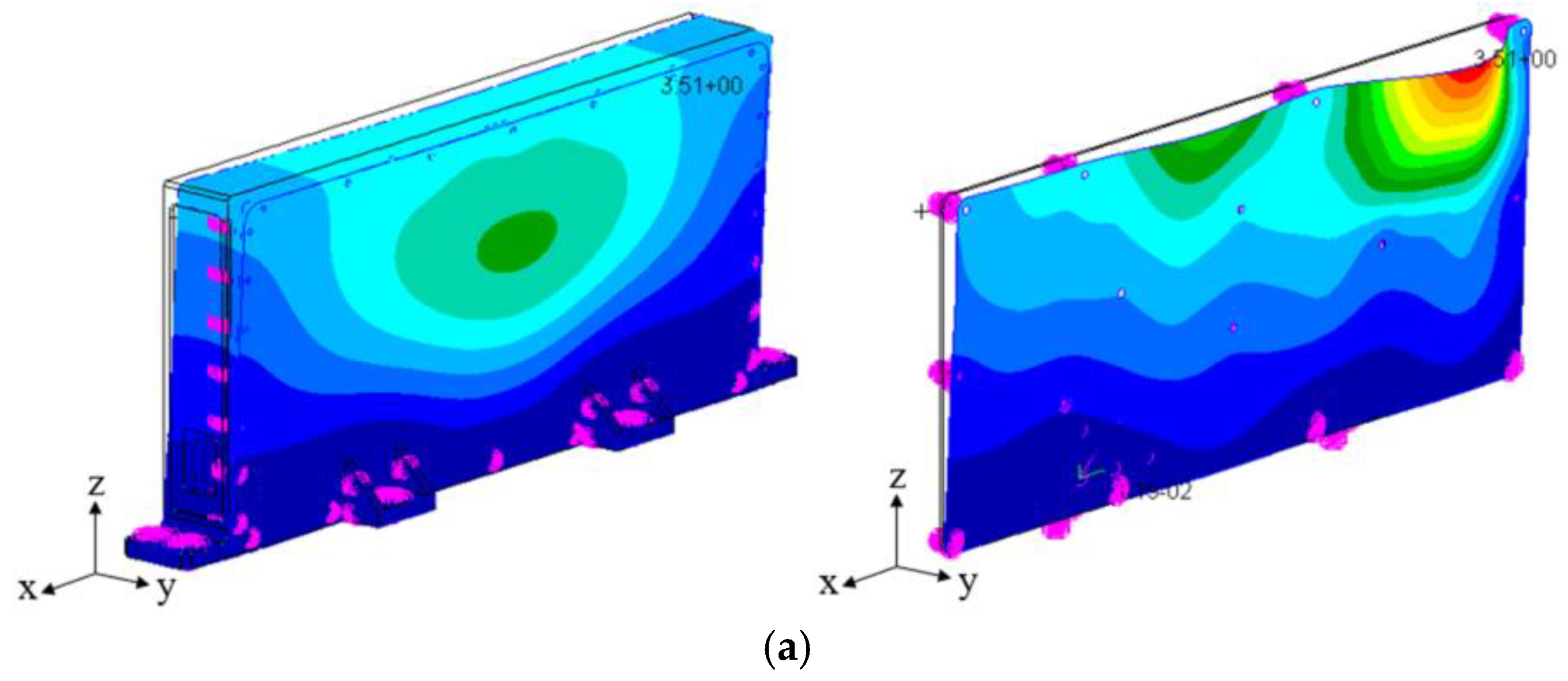
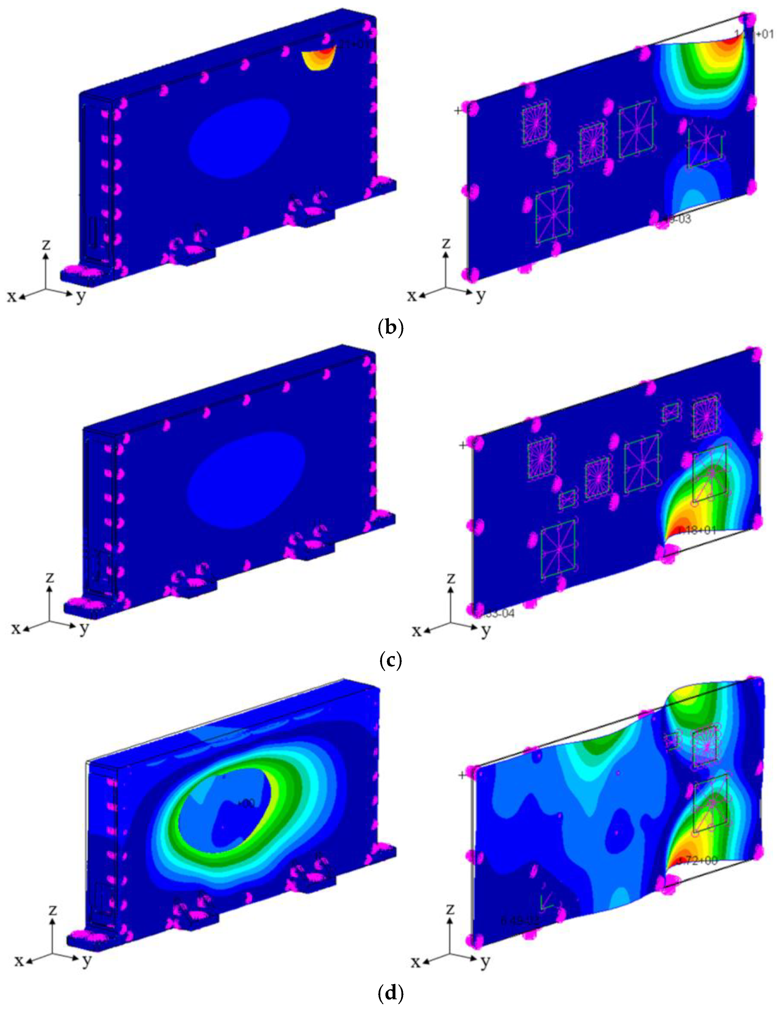
ε p m a x is the average strain at each corner. The methodology presented in this study is an integral part of the Oh-Park methodology and was used to evaluate the structural safety of solder joints in comprehensive PCB specimens. A modal analysis was performed on the constructed finite element model, and the natural frequency of the most vulnerable first mode was 298.5 Hz. The corresponding mode shape is as shown in Figure 9. A random vibration analysis was performed according to these mode shapes to evaluate the structural safety of the solder joints for each electronic package, and the results were compared with those from the fatigue-life test.

4.2. Analysis and Test Results

To predict and evaluate structural safety based on the Oh-Park methodology, various conditions for test and launch process procedures were established. It was assumed that spaceborne electronic equipment is exposed to random vibrations in three stages: component level qualification test, satellite system level qualification test, and launch. The vibration test was first performed by sequentially increasing the excitation levels for each axis to −12 dB, −9 dB, −6 dB, −3 dB, and finally 0 dB. Fifteen tests were conducted, and calculations were performed to convert the test into an equivalent test duration for 0 dB. This calculation is expressed as a 0 dB equivalent because structural analyses typically use the 0 dB standard random vibration as input for evaluating spaceborne electronic equipment. Here, the 0 dB standard corresponds to the qualification-level test condition. In this way, the 0 dB equivalent time for qualification test, acceptance test, and launch was calculated. Acceptance testing usually excludes the 0 dB test from the calculation because it is a −3 dB standard compared to the qualification test. For the launch phase, the equivalent time was calculated assuming that −3 dB vibration occurred simultaneously on each axis, and the duration was 4 min [31]. Based on the above procedures and formulas, T T F r e q was calculated, as listed in Table 5, and design methodology was validated using the experimental results obtained in this study and this assumed value.
Table 6 presents the calculation results for each electronic package type, along with the first mode frequency of the eight electronic packages on the comprehensive PCB specimen. The table also includes the results of the solder joint structural safety evaluation derived from both Steinberg’s theory and Oh-Park methodology.
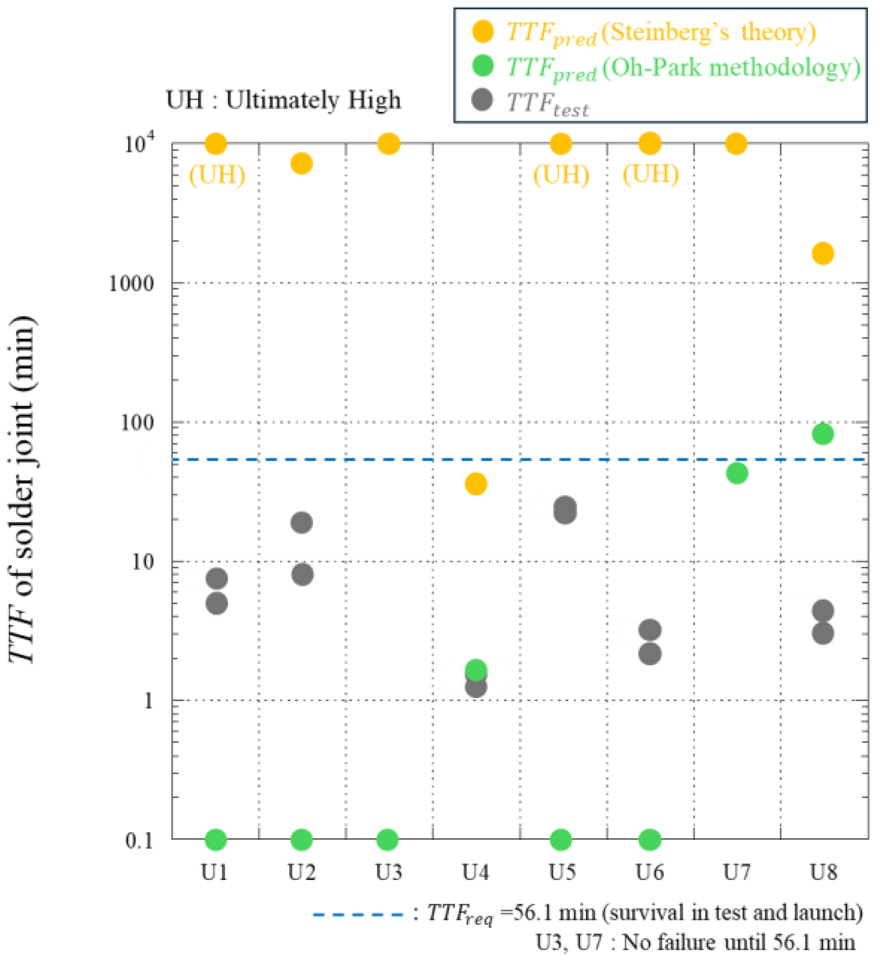
Table 7 and Figure 10 present the T T F p r e d estimated using each methodology and the actual test results T T F t e s t .
The structural safety assessment was used to calculate the PCB critical strain ( ε c ) for each electronic package. In addition, the PCB allowable strain ( ζ ) and PCB strain ( ε ˙ ) used to calculate the PCB critical strain reflected the natural frequency ( f n ) derived for each element from the mode analysis results. Moreover, to derive the PCB maximum strain ( ε p m a x ), RMS nodal strain analysis was performed, and the average RMS values, which were derived from the nodes corresponding to the four corners of the electronic package mounting area in the vertical, and shear directions were considered [17]. The result values were compared with the MoS calculation values obtained using Steinberg theory, which is the conventional structural safety evaluation method. For MoS calculated using Steinberg’s theory, positive margins were observed for all cases except for one package. In contrast, MoS calculated using the Oh-Park methodology showed negative margins in all cases except for one package. During actual testing, all electronic packages, except U3 and U7, failed indicating that Steinberg’s theory produced overly optimistic results. In addition, the Steinberg’s theory overestimated the T T F p r e d compared to the T T F t e s t output value and the T T F p r e d estimated by Oh-Park methodology. This discrepancy arises because Steinberg’s theory involves imprecise boundary conditions when calculating allowable displacement, resulting in uncertainty and low reliability under these conditions.
In contrast, the Oh-Park methodology, which is based on the critical strain, produced more reasonable and accurate results, closely matching the test outcomes. For packages that did not fail, the continuous random vibrations during testing likely caused cumulative damage to the solder joints, thereby gradually mitigating the deformation response transmitted to the surrounding packages. This phenomenon is affected by complex factors such as changing conditions and boundary effects, which are difficult to interpret. The results indicate that the Oh-Park methodology provides a more reliable structural safety evaluation than the Steinberg’s theory. In addition to its technical validation, the proposed methodology offers practical benefits for spacecraft design. The engineering-qualification model (EQM) of spaceborne electronic equipment is generally not used as a flight model (FM) because of the stresses it experiences during testing. However, the proposed methodology can be considered for FM applicability when MoS guarantees that structural safety is judged by considering the accumulated time in the test and launch environments according to the proposed method. This significantly reduces development costs and is advantageous for implementing low-cost satellites in line with the low-cost mass production flow demanded by the Newspace trend.

5. Conclusions

In this study, the structural safety of solder joints in vertically mounted spaceborne electronic equipment was evaluated using the critical strain-based Oh-Park methodology. Thus, the validity of the methodology was verified. Unlike the conventional Steinberg’s theory, which relies on simplified boundary conditions and fixed fatigue life criteria, the Oh-Park methodology reflects the PCB strain response, cumulative fatigue cycles during testing and firing stages, and boundary conditions. Fatigue life tests using a comprehensive PCB specimen including PBGA928, QFP208, and TSOP48 packages and vertically mounted housing showed that the Oh-Park methodology accurately predicted failures in five of eight packages and produced fatigue lives that closely matched the test results. In contrast, Steinberg’s theory overestimates the MoS in most packages and does not sufficiently reflect the local strain and multimode interactions that appear in vertical mounting. The strength of the Oh-Park methodology is that it enables accurate fatigue life prediction even in complex structural configurations by reflecting boundary condition variations between multiple packages and global-local mode coupling effects, and that it can maintain accuracy while securing analysis efficiency through a simplified finite element modeling technique. Furthermore, unlike previous studies that verified the methodology, this study expanded the verification scope to a multi-package configuration similar to the actual, thereby demonstrating its applicability to the design of actual spaceborne electronic equipment. In summary, Oh-Park methodology has been validated as a reliable and efficient design methodology for designing vertically mounted spaceborne electronic equipment, with improved predictive accuracy and practical applicability compared to Steinberg’s theory.

Author Contributions

Conceptualization, H.-U.O.; methodology, H.-U.O.; validation, J.-C.H., K.-W.K. and H.-U.O.; formal analysis, J.-C.H. and K.-W.K.; investigation, J.-C.H. and H.-U.O.; data curation, J.-C.H. and K.-W.K.; writing—original draft preparation, J.-C.H.; writing—review and editing, J.-C.H. and H.-U.O.; visualization, J.-C.H.; supervision, H.-U.O.; project administration, H.-U.O.; funding acquisition, H.-U.O. All authors have read and agreed to the published version of the manuscript.

Funding

This work was supported by a Korea Research Institute for Defense Technology Planning and Advancement (KRIT) grant funded by the Korean government Defense Acquisition Program Administration (DAPA) (KRIT-CT-22-040, Heterogeneous Satellite Constellation based ISR Research Center, 2022).

Data Availability Statement

The data used to support the findings of this study are available from the corresponding author upon request.

Conflicts of Interest

The authors declare no conflict of interest.

References

  1. Kim, Y.K.; Hwang, D.S. PBGA packaging reliability assessments under random vibrations for space applications. Microelectron. Reliab. 2015, 55, 172–179. [Google Scholar] [CrossRef]
  2. Jang, T.S.; Cho, H.K.; Seo, H.S.; Kim, W.S.; Rhee, J.H. Lightweight composite electronics housing design of modular type for space applications. J. Korean Soc. Aeronaut. Space Sci. 2010, 38, 1209–1216. [Google Scholar] [CrossRef]
  3. Krumweide, G.C.; Tremblay, G.A. Issues to Address in Use of Composite Materials for Electronic Packaging. In Proceedings of the 17th Digital Avionics Systems Conference, Bellevue, WA, USA, 31 October–7 November 1998; pp. H35-1–H35-8. [Google Scholar]
  4. Fenske, M.T.; Barth, J.L.; Didion, J.R.; Mul, P. The development of lightweight electronics enclosures for space applications. SAMPE J. 1999, 35, 25–34. [Google Scholar]
  5. Aglietti, G.S. A Lighter enclosure for electronics for space application. Proc. Inst. Mech. Eng. Part G J. Aerosp. Eng. 2002, 216, 131–142. [Google Scholar] [CrossRef]
  6. Wijker, J.J. Spacecraft Structures; Springer Science & Business Media: Berlin/Heidelberg, Germany, 2008. [Google Scholar]
  7. Lee, W.B.; Kim, G.W. Random vibration analysis for satellite design. Aerosp. Eng. Technol. 2006, 5, 102–107. [Google Scholar]
  8. Meyyappan, K.; Vujosevic, M.; Wu, Q.; Malatkar, P.; Hill, C.; Parrott, R. Knowledge Based Qualification Process to Evaluate Vibration Induced Failures in Electronic Components. In Proceedings of the ASME 2017 International Technical Conference and Exhibition on Packaging and Integration of Electronic and Photonic Microsystems Collocated with the ASME 2017 Conference on Information Storage and Processing Systems, San Francisco, CA, USA, 29 August–1 September 2017; p. V001T05A001. [Google Scholar]
  9. Lee, W.W.; Nguyen, L.T.; Selvaduray, G.S. Solder joint fatigue models: Review and applicability to chip scale packages. Microelectron. Reliab. 2000, 40, 231–244. [Google Scholar] [CrossRef]
  10. Fan, X.; Ranouta, A.S.; Dhiman, H.S. Effects of package level structure and material propreties on solder joint reliability under impact loading. IEEE Trans. Compon. Packag. Manuf. 2012, 3, 52–60. [Google Scholar] [CrossRef]
  11. García, A.; Sorribes-Palmer, F.; Alonso, G. Application of Steinberg vibration fatigue model for structural verification of space instruments. AIP Conf. Proc. 2018, 1922, 100003. [Google Scholar] [CrossRef]
  12. Steinberg, D.S. Vibration Analysis for Electronic Equipment, 3rd ed.; John Wiley & Sons: New York, NY, USA, 2000. [Google Scholar]
  13. Bèda, M.G. A curvature-based interpretation of the Steinberg criterion for fatigue life of electronic components. Int. Symp. Microelectron. 2015, 2015, 707–712. [Google Scholar] [CrossRef]
  14. Kavitha, M.; Mahmound, Z.H.; Kishore, K.H.; Petrov, A.M.; Lekomtsev, A.; Iliushin, P.; Zekiy, A.O.; Salmani, M. Application of Steinberg model for vibration lifetime evaluation of Sn-Ag-Cu-based solder joints in power semiconductors. IEEE Trans. Compon. Packag. Manuf. Technol. 2021, 11, 444–450. [Google Scholar] [CrossRef]
  15. Jeon, Y.-H.; Kim, H.-S.; Lim, I.-O.; Kim, Y.; Oh, H.-U. Mechanical reliability evaluation on solder joint of CCB for compact advanced satellite. J. Korean Soc. Aeronaut. Space Sci. 2017, 45, 498–507. [Google Scholar] [CrossRef]
  16. Irvine, T. Extending Steinberg’s Fatigue Analysis of Electronics Equipment Methodology to a Full Relative Displacement vs. Cycles Curve. Vibrationdata. 2013. Available online: https://www.vibrationdata.com/tutorials2/electronic_rd_n.pdf (accessed on 1 May 2025).
  17. Park, T.Y.; Oh, H.U. New PCB strain-based structural design methodology for reliable and rapid evaluation of spaceborne electronics under random vibration. Int. J. Fatigue 2021, 146, 106094. [Google Scholar] [CrossRef]
  18. Kim, J.K.; Chae, B.G.; Lee, S.H.; Oh, H.U. Structural design of SAR control units for small satellites based on critical strain theory. J. Aerosp. Syst. Eng. 2024, 18, 12–20. [Google Scholar]
  19. Park, J.H.; Jeong, S.K.; Oh, H.U. Effectiveness of critical-strain-based methodology considering elastic mode vibration of mechanical housing of electronics. Aerospace 2023, 10, 974. [Google Scholar] [CrossRef]
  20. Kwon, S.C.; Son, J.H.; Song, S.C.; Park, J.H.; Koo, K.R.; Oh, H.U. Innovative mechanical design strategy for actualizing 80 kg-class X-band active SAR small satellite of S-STEP. Aerospace 2021, 8, 149. [Google Scholar] [CrossRef]
  21. Kang, S.J.; Park, S.W.; Choi, H.Y.; Ryu, G.H.; Kim, J.P.; Jung, S.H.; Kim, S.Y.; Lee, H.I.; Oh, H.U. Thermo-Mechanical Design and Validation of spaceborne High-Speed Digital Receiver Unit for Synthetic Aperture Rader Application. Aerospace 2021, 8, 305. [Google Scholar] [CrossRef]
  22. Yin, Q.; Xue, F.; Shen, L. Structural design and mechanical analysis for space-borne electronic equipment. J. Phys. Conf. Ser. 2023, 2492, 012009. [Google Scholar] [CrossRef]
  23. Zhang, L.; Liu, J.; Guo, H.; Wang, S.; Liang, D.; Yu, L. Thermo design technology of spaceborne radar electronic unit. J. Phys. Conf. Ser. 2025, 2955, 012054. [Google Scholar] [CrossRef]
  24. An, J.H.; Cho, H.K. structural and thermal analyses of image processing units of satellites. J. Korean Soc. Manuf. Technol. Eng. 2020, 29, 42–50. [Google Scholar] [CrossRef]
  25. Jang, T.S.; Seo, J.K.; Rhee, J.H. A study on fabrication of monolithic lightweight composite electronics housing for space application. J. Korean Soc. Aeronaut. Space Sci. 2013, 41, 975–986. [Google Scholar] [CrossRef]
  26. Kim, J.K.; Park, T.Y.; Oh, H.U. dynamic response analysis with electronics mounting boundary conditions. J. Aerosp. Syst. Eng. 2024, 18, 9–15. [Google Scholar]
  27. Kim, K.W.; Park, J.H.; Park, T.Y.; Oh, H.U. Experimental evaluation of the effectiveness of the printed circuit board strain-based methodology in space-borne electronics with vertically mounted printed circuit boards. Aerospace 2024, 11, 562. [Google Scholar] [CrossRef]
  28. Jung, I.H.; Park, T.W.; Han, S.W.; Seo, J.H.; Kim, S.H. Structural vibration analysis of electronic equipment for satellite under launch environments. J. Korean Soc. Precis. Eng. 2004, 21, 120–128. [Google Scholar] [CrossRef]
  29. Clerck, J.D.; Epp, D.S. Rotating Machinery, Hybrid Test Methods, Vibro-Acoustics & Laser Vibrometry. In Proceedings of the 34th IMAC, A Conference and Exposition on Structural Dynamics, Orlando, FL, USA, 25–28 January 2016. [Google Scholar]
  30. ECSS-E-ST-32C; Space Engineering—Structural General Requirements. European Cooperative Space Standards: Noordwijk, The Netherlands, 2008.
  31. Yunis, I.; Ludwiczak, D. On the use of 3dB qualification margin for structural parts on expendable launch vehicles. In Proceedings of the 48th AIAA/ASME/ASCE/AHS/ASC Structures, Structural Dynamics, and Materials Conference, Honolulu, HI, USA, 23–26 April 2007; pp. 1–9. [Google Scholar]
  32. IPC. IPC-9701A: Performance Test Methods and Qualification Requirements for Surface Mount Solder Attachments; IPC: Bannockburn, IL, USA, 2006. [Google Scholar]
  33. Jeong, H.S.; Seo, K.W.; Bae, J.S.; Jang, G.H. Effect of boundary conditions on fatigue life of board-level BGA solder joints under random vibration. Microsyst. Technol. 2023, 29, 1651–1658. [Google Scholar] [CrossRef]
  34. Lee, J.S.; Jeong, H.S.; Jang, G.H. Optimization of the Boundary Conditions of a Board Level Reliability Test Board to Maximize the Fatigue Life of Ball Grid Array Solder Joints under Thermal Cycling and Random Vibration. Materials 2024, 17, 755. [Google Scholar] [CrossRef] [PubMed]
  35. Park, T.Y.; Park, J.H.; Oh, H.U. Experimental evaluation of vibrational stability of SOPs in aerospace industry using PCB strain effectiveness of a PCB-strain-based design methodology. Aerospace 2023, 10, 516. [Google Scholar] [CrossRef]
  36. Park, T.Y.; Oh, H.U. Validation of the critical strain-based methodology for evaluating the mechanical safety of ball grid array solder joints in a launch random vibration environment. J. Electron. Packag. 2022, 144, 011006. [Google Scholar] [CrossRef]
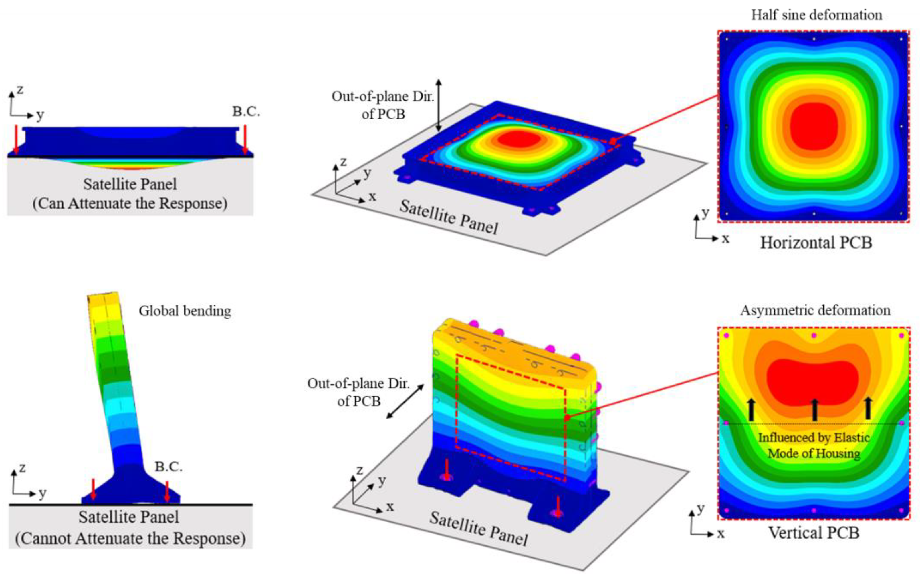
Figure 1. Comparison schematic between horizontal and vertical mounted spaceborne electronic equipment.
Aerospace 12 00770 g001
Figure 2. Structure for spaceborne electronic equipment module.
Aerospace 12 00770 g002
Figure 3. Comprehensive PCB specimen configuration.
Aerospace 12 00770 g003
Figure 4. Fatigue-life test setup for spaceborne electronic equipment module.
Aerospace 12 00770 g004
Figure 5. Time profile of measured daisy-chain resistance of each package for Sample 1 during random vibration excitation.
Aerospace 12 00770 g005
Figure 6. Time profile of measured daisy-chain resistance of each package for Sample 2 during random vibration excitation.
Aerospace 12 00770 g006
Figure 7. Finite element modeling for spaceborne electronic equipment module: (a) with cover; (b) without cover.
Aerospace 12 00770 g007
Figure 8. Simplified modeling for electronic packages: (a) PBGA928 (9 nodes); (b) QFP208 (16 nodes); (c) TSOP48 (6 nodes).
Aerospace 12 00770 g008
Figure 9. Representative mode shapes of housing module and PCB specimen: (a) 1st mode: 298.5 Hz; (b) 2nd mode: 377 Hz; (c) 3rd mode: 417.2 Hz; (d) 4th mode: 436.11 Hz.
Aerospace 12 00770 g009aAerospace 12 00770 g009b
Figure 10. Comparison between T T F t e s t and T T F p r e d obtained using Steinberg’s theory and Oh-Park methodology for each package (U1–U8: see package types in Figure 3).
Aerospace 12 00770 g010
Table 1. Specifications of PBGA928, QFP208 and TSOP48.
ItemSpecifications
PBGA928Dimension (mm): 40 × 40 × 2.23
Aerospace 12 00770 i001Weight (g): 6.7 (Incl. solder balls)
No. of solder balls: 928
Ball pitch (mm): 1.0
Solder material: Tin/lead
QFP208Dimension (mm): 28 × 28 × 3.7
Aerospace 12 00770 i002Weight (g): 5.4
Leads: Cu Lead Frame with Lead Finish
Lead pitch (mm): 0.5
Solder material: Sn-Pb37
TSOP48Dimension (mm): 18.4 × 12 × 1.2
Aerospace 12 00770 i003Weight (g): 0.6
Leads: Cu Lead Frame with Lead Finish
Lead pitch (mm): 0.5
Solder material: Sn-Pb37
Table 2. Specifications of input random vibration.
Frequency (Hz)ASD (g2/Hz)
200.052
500.32
8000.32
20000.052
Overall (full level (0 dB))20 grms
Table 3. T T F time measured in fatigue-life test.
Package No.Sample 1 (s)Sample 2 (s)
U1 (PBGA928)439305
U2 (PBGA928)1153502
U3 (PBGA928)No faliureNo faliure
U4 (QFP208)9076
U5 (QFP208)14871331
U6 (QFP208)190134
U7 (TSOP48)No faliureNo faliure
U8 (TSOP48)270183
Table 4. Material property information used in finite element modeling.
MaterialElastic Modulus (GPa)Poisson’s RatioDensity (kg/m3)
PCB (FR-4)18.730.1361850
Housing Module (A6061-T6)68.900.3302700
Table 5. Estimation Results of T T F r e q for survial of solder joint in test and launch process.
ItemFactorValueUnitRemarks
No. of vibration tests per each test levelN3-Assumption (damage for PCB out-of-plane excitation is accumulated in all test axis)
Fatigue exponent for solder jointB6.4-for solder or lead frame material
0 dB-equivalent vibration exposure time for the vibration tests at each test levelT−12dB0.00007minEquations (9) and (10)
T−9dB0.0007min
T−6dB0.006min
T−3dB0.11min
T0dB2.00min
Duration for single test (min)t10.50minfor low level tests (−12, −9, −6 dB)
t21.00minfor accp. test (−3 dB)
tQ2.00minfor qual. test (0 dB)
0 dB-equivalent vibration exposure time for qual. test (comp. level)ΣTC-Q6.35min-
0 dB-equivalent vibration exposure time for qual. test (S/S level)ΣTS/S-Q6.35min-
Eqv. time for launch (S/S level)ΣTL1.32minEqv. to AT (ΣD−3dB),
3 axis excitations
0 dB-equivalent vibration exposure time for the launch vibration (min)tL4.00minfor launch
FoS with respect to. design life (min)FoSttf4-Referred ECSS-E-ST-32C [30]
Design   life   ( T T F ) for solder joint (min)TTFreq56.1minEquation (7)
Table 6. Comparative results of structural safety evaluation for each package (U1–U8: see package types in Figure 3).
(a) Steinberg’s Theory
Package
No.
Package Type f n Allowable DisplacementMax. Disp.Structural SafetyTest
Results
r d δ a l l o w δ m a x D F M o S
Hz-mmmmmm--
U1PBGA928298.50.4781500.3970.156 1.60 3.07Failed
U2PBGA928298.50.947 1500.200 0.150 1.60 1.14Failed
U3PBGA928298.50.5351500.3540.034 1.60 15.73Not Failed
U4QFP208298.50.4521500.6971.190 1.60 −0.06Failed
U5QFP208298.50.960 1500.3280.116 1.60 3.52Failed
U6QFP208298.50.4361500.7230.136 1.60 7.51Failed
U7TSOP48298.50.8541500.4550.098 1.60 6.44Not Failed
U8TSOP48298.50.5031500.7730.730 1.60 0.69Failed
(b) Oh-Park methodology
Package No.Package Type f n Critical StrainMax. StrainStructural SafetyTest
Results
ε d o t ζ ε c ε p m a x D F M o S
Hz μ s t r . / s μ s t r . μ s t r . μ s t r . --
U1PBGA928298.51.08 × 10698.0 44.6 574.11.60 −0.88Failed
U2PBGA928298.57.60 × 105147.1 67.0 405.21.60 −0.74Failed
U3PBGA928298.57.92 × 105141.4 64.4 422.21.60 −0.76Not Failed
U4QFP208298.56.63 × 105166.5 125.8 353.41.60 −0.43Failed
U5QFP208298.58.17 × 105137.0 103.6 435.51.60 −0.62Failed
U6QFP208298.51.07 × 10698.5 74.4 572.11.60 −0.79Failed
U7TSOP48298.55.55 × 106191.5 178.5 296.11.60 −0.04Not Failed
U8TSOP48298.55.23 × 105200.0 186.5 278.81.60 0.07Failed
Table 7. Comparison between T T F t e s t and T T F p r e d calculated using Steinberg’s theory and Oh-Park methodology for each package (U1–U8: see package types in Figure 3).
Package No.Steinberg’s Theory
T T F p r e d (min)
Oh-Park Methodology
T T F p r e d (min)
T T F t e s t (min)
Sample 1Sample 2
U1440,000<17.325.08
U27110<119.228.37
U33,730,000,000<1No failureNo failure
U436.51.51.501.27
U5862,000<124.7822.18
U649,500,000<13.172.23
U720,900,00043.8No failureNo failure
U81610854.503.05
Disclaimer/Publisher’s Note: The statements, opinions and data contained in all publications are solely those of the individual author(s) and contributor(s) and not of MDPI and/or the editor(s). MDPI and/or the editor(s) disclaim responsibility for any injury to people or property resulting from any ideas, methods, instructions or products referred to in the content.