Article

Image Processor and RISC MCU Embedded Single Chip Fingerprint Sensor

School of Information Science and Telecommunication, Hanshin University, 137 Hanshindae-gil, Osan-si 18101, Korea
J. Sens. Actuator Netw. 2020, 9(4), 51; https://doi.org/10.3390/jsan9040051
Submission received: 28 August 2020 / Revised: 29 October 2020 / Accepted: 30 October 2020 / Published: 2 November 2020

Abstract

:
In this paper, we propose a single chip fingerprint sensor with the algorithm processor and 16-bit MCU. The algorithm processor is a logic circuit that implements the GABOR filter and the THINNING step, which occupies 80% of the fingerprint image processing time. The rest of the algorithm is processed by embedded 16-bit MCU with small circuit volume, so all steps of the algorithm can be processed on the single chip without an external CPU. The capacitive sensing circuit was designed by applying the parasitic-insensitive integrator with the variable clock generator. The function was verified by Cadence Spectre for a 1-pixel sensor scheme and RTL and post simulation for digital blocks synthesized by Synopsys Design Compiler in 180n 2-poly 6-metal CMOS (complementary metal–oxide–semiconductor) process. The layout is done by automatic P&R for the full chip in a 96 × 96 pixel array. The chip area is 5010 μm × 5710 μm (28.61 mm2) and the gate count is 2,866,700. The result is compared with a conventional one. The proposed scheme can reduce the processing time by 57%.

1. Introduction

Fingerprint is the most popular biometric method for authentication. Minutiae-based fingerprint recognition algorithms are widely used. Minutiae means the position and angle information of ending and ridge bifurcation. The image captured from the sensor is processed through an algorithm as shown in Figure 1. The fingerprint algorithm is divided into a process of registering an existing fingerprint and a step of confirming identity by matching a new fingerprint and a registered fingerprint [1,2,3]. Both steps go through a complex procedure of applying an algorithm and extracting feature points. In order to extract the feature points, pre-processing, feature point extraction, and matching are required. To date, various methods have been proposed mainly for software-oriented fingerprint image processing. A high-performance processor and processing time are required for such a complex algorithm. In order to perform the matching process on a large number of fingerprint images, the fast speed of image analysis is important [4,5,6]. One of the ways to get an obvious increase in speed is the hardware implementation of the algorithm [4,7,8,9,10,11,12,13,14]. In general, a sensor and an algorithm are separated in a fingerprint recognition system. There are many advantages if the sensor and algorithm can be operated on a single chip. Currently, the processing speed of the fingerprint recognition sensor applied to the general security system is around 500 ms. In particular, when applied to mobile, a processing speed of 500 ms or less is required. Embedded fingerprint identification systems require high-performance microcontrollers such as 32-bit or 64-bit CPUs. This is expected to reduce the operating speed and implement a small fingerprint identification system through the application of the hardware-oriented method.
Several attempts have been made in the hardware development of fingerprint recognition algorithms for each step of the algorithm [7,8,9,10,11,12,13,14]. The papers deal with the hardware implementation of Gabor filters [7,8,9,10] and thinning [13,14], respectively, or a combination of two stages [11,12], while the final implementation is limited to simulation and FPGA (Field Programmable Gate Array) verification. Although VLSI implementation has been proposed [9,10], it is only a simulation, and there is no case in which the entire algorithm and MCU are integrated on single chip. Since there are differences in target device, image size, process conditions, etc., it is difficult to compare performance with old research results [7,8,9,10,11,12,13,14] for the two stages implemented in hardware. Therefore, instead of step-by-step performance comparison, this will be dealt with in terms of improved processing time and increased chip area when implemented with an integrated single VLSI chip.
In this paper, we propose a single-chip fingerprint sensor structure with a built-in algorithm processor and small MCU. The CPU occupancy of the algorithm was analyzed using the ARM emulator and the FPGA environment. The algorithm processor handles only the binarization and thinning step. The 16-bit RISC MCU handles the remaining steps that are processed by software. The algorithm processor is designed by applying the Gabor filter for binarization and the ZS (Zhang-Suen) algorithm for thinning [15]. The rest of the algorithm is processed by an embedded 16-bit MCU with a small circuit volume, so all steps of the algorithm can be processed on a single chip without an external CPU. The operation of the circuit was verified by Cadence Spectre for a 1-pixel sensor system in 0.18 μm standard CMOS process and 1.8 V power condition, and the logic synthesis circuit using Synopsys Design Compiler was performed by RTL and post layout simulation. The layout is done by a full custom flow for the sensor cell array and automatic P&R for the entire chip.

2. Sensor Array Design

2.1. Sensor Design

As shown in Figure 2 [16,17,18,19], a capacitive sensing circuit is introduced. The difference in capacitance between a ridge and valley is very small, with a few femtofarads. This circuit is designed to detect weak capacitances by using a non-overlapping clock to eliminate the effect of parasitic capacitance. The sensor plate is shielded with a second metal to prevent noise from occurring in the circuit under the sensor plate, which forms a parasitic capacitance between the sensor plate and the metal shield. The parasitic capacitance Cp1 is very large compared to the finger capacitance Cf and must be removed. To eliminate this parasitic capacitance, we apply an output to the lower node of Cp1 to maintain the same potential between the two nodes of Cp1, maximizing the sensitivity of the fingerprint sensor. The operational amplifier acts like a buffer between the top metal with Cp1 and the shield metal.
Figure 2b shows the pattern of sensor output signals in the ridge and valley of the fingerprint. Because the capacitance at the ridge is greater than the valley, the output of the integrated signal is different. The integration signal is decreased much more slowly in the valley. The proposed circuit is resistant to noise and is advantageous in recognizing fingerprints with high sensitivity with low power, but it takes a long time to integrate charges. As a result of the simulation, the proposed sensing circuit requires a maximum of 112 clocks to charge the full range voltage. It needs about 0.922 s to obtain a 96 × 96 image frame at 10 MHZ. This is very long time, but the disadvantage can be solved through a pipelined charge integration method.

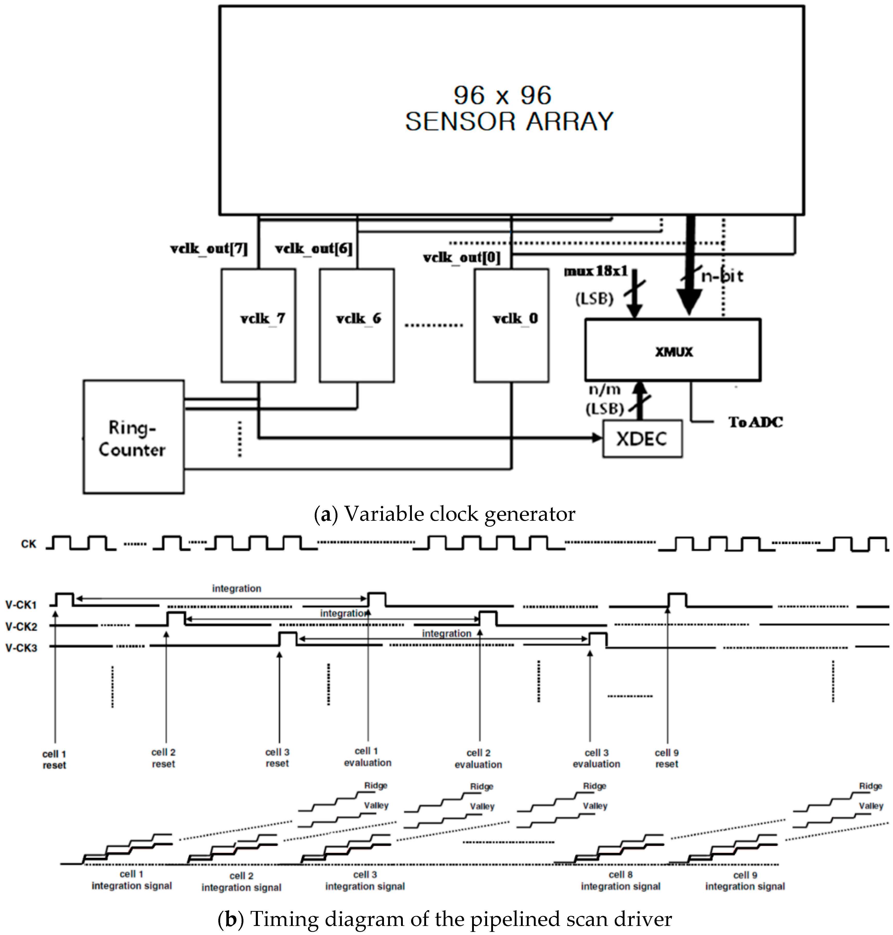
2.2. Sensor Array Design

A pipeline type control circuit is applied to simultaneously detect the next pixel before the integration of one pixel is completed. The pipelined scan driver can reduce image capture time dramatically. Figure 3 shows 96 × 96 array fingerprint sensor with the pipelined scan driver architecture [20]. Figure 3b shows the timing diagram of the pipelined scan driver. v-ck1 to v-ck8 are column control signals. This signal generates or resets the evaluation signal for the cell. The same clock signal is generated every eight cells. Therefore, we can expand the depth of the pipeline scan to evaluate eight cells simultaneously. Eight shift ring counters select the column clock generator every 16 clock intervals. The sensor cell is designed to be evaluated every 16 clocks. Thus, it is possible to effectively reduce the fingerprint image capture time without damaging the original signal. The fingerprint sensor consists of a sensor cell array, shift ring counter, multiplexer, and decoder. The shift ring counter generates a pipeline scan signal. The multiplexer selects the column output for the sensor cell. The ADC converts the sense signal output to gray-scale. The analog signal is fed to the ADC through an analog multiplexer. The proposed circuit provides three pipeline scan modes. v-ck1 generates a reset signal for the first sensor cell, then the evaluation of the first sensor cell begins, then v-ck2 generates a reset signal for the second sensor cell, and the evaluation of the second sensor cell proceeds simultaneously. The 9th sensor cell receives the reset signal generated by v-ck1. As a result, the evaluation of the sensor cell is performed every 16 clocks. As shown in Figure 3, the sensing signal is integrated to increase the output voltage of the sensor cell linearly.

3. Analysis of Fingerprint Algorithm

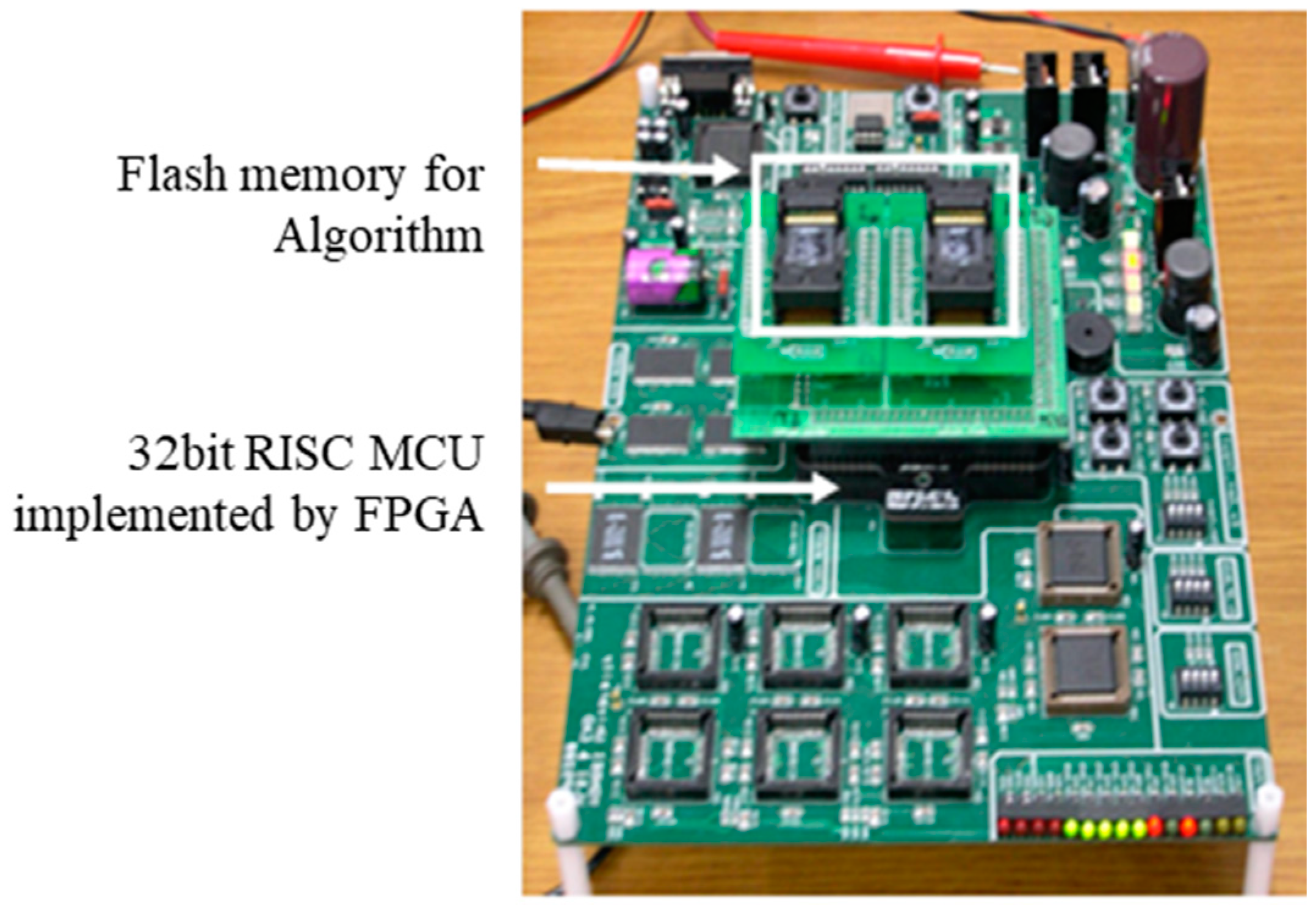
We built an FPGA environment and implemented a general-purpose ARM7 compatible RISC microcontroller to verify the correct operation of the Minutiae-based fingerprint algorithm. The applied fingerprint algorithm is based on Jain’s references [3,21,22,23]. Figure 4 shows the FPGA emulation board for algorithm verification. The sample image is a FVC2002 DB modified to a size of 96 × 96 pixels at 500 dpi. A point routine is inserted in the lower right corner of the board to check each step of the identification algorithm. The checkpoint routine turns on one of the eight LEDs in succession. Finally, we confirmed that the embedded 32-bit RISC core successfully performed the fingerprint authentication algorithm. All results of the algorithm instructions are compared with the results of the ARM emulator, the software emulator of the ARM processor.
Table 1 shows the results of the ARM emulation. The algorithm’s total CPU cycle was 4.64 M in 96 × 96 sample images. Gabor filters and Thinning algorithms occupy about 80% of the entire cycle. A description of each step of the algorithm is shown in Figure 1. Here, I-cycle means an internal cycle and the microprocessor does not request a transfer because it executes an internal instruction. N-cycle means non-sequential period, and the microprocessor sends a request to an address regardless of the address used in the previous cycle. S-cycle is a sequential period, where the microprocessor sends a request to an address with a word or half word after the previous address, or to the same address.

4. Algorithm Processor and MCU Design

4.1. Gabor Filter Design

Gabor filters are linear filters used for feature extraction, texture analysis, edge detection, and more. Gabor filters are used in many image processing applications. Gabor filters have frequency and direction information and have optimal coupling resolution in spatial and frequency dimensions. Therefore, it is appropriate to use a Gabor filter as a band pass filter to remove noise and recover the improved ridge and valley structures [21,22]. Figure 5 shows an example of a Gabor wavelet and 40 filter banks with five frequencies and eight directions.
The input image is divided into non-overlapping window sizes in order to calculate the Gabor filter coefficients. In this study, the window size of the Gabor filter kernel is 11 × 11. The Gabor filter is calculated based on the angle (θ) and frequency(f) of the ridge obtained through the block ridge orientation and frequency estimation steps shown in Figure 1. Gabor filters are two-dimensional filters made of Gaussian and cosine functions and have the following general form
h ( x , y : θ , f ) = exp [ 1 2 ( x θ 2 σ x 2 + y θ 2 σ μ 2 ) ] cos ( 2 π fx θ )
x θ = xcos θ + ysin θ y θ = ycos θ xsin θ
where x and y are the pixel positions on the entire image and σx and σy are Gaussian space constants. Appropriate care should be taken in determining the values of σx and σy. The smaller the value, the less likely it is to generate false ridges and valleys. The higher the value, the stronger the noise, but there is a possibility of generating wrong ridges and valleys. Therefore, the noise reduction effect is less. In this study, the mentioned parameters were analyzed and the values of σx and σy were set to 4.0.
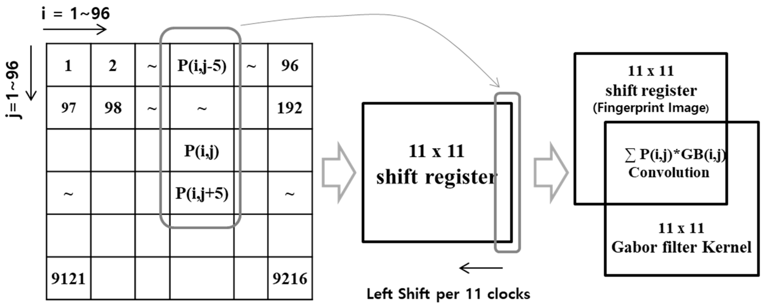
Cosine, sine and exponential functions are required for kernel calculation. In this study, a look-up table was applied to enable high-speed calculation for trigonometric function. It was designed in 0~2 π at 0.03 radian intervals. The exponential function also applied a look-up table rather than applying an IP requiring large chip area and complex operation. Pre-analysis was performed to predict the exponential function input range. As a result of applying the average frequency and orientation value of the fingerprint to Equation (2), the input range is −80 to 80, and an interval of 6.28 is applied. The functional block of the Gabor filter is shown in Figure 6. The designed circuit generates an address of memory that matched with 11 vertical images of the block image P(i,j). The proposed circuit transfers the images to the 2D shift register every 11 clock cycles and then performs a left shift operation. The designed circuit performs convolution by applying a shift register and Gabor filter. If the convolution result is positive, P(i,j) means valley and if it is negative, P(i,j) means ridge. The final output image is binary format.

4.2. Thinning Algorithm Design

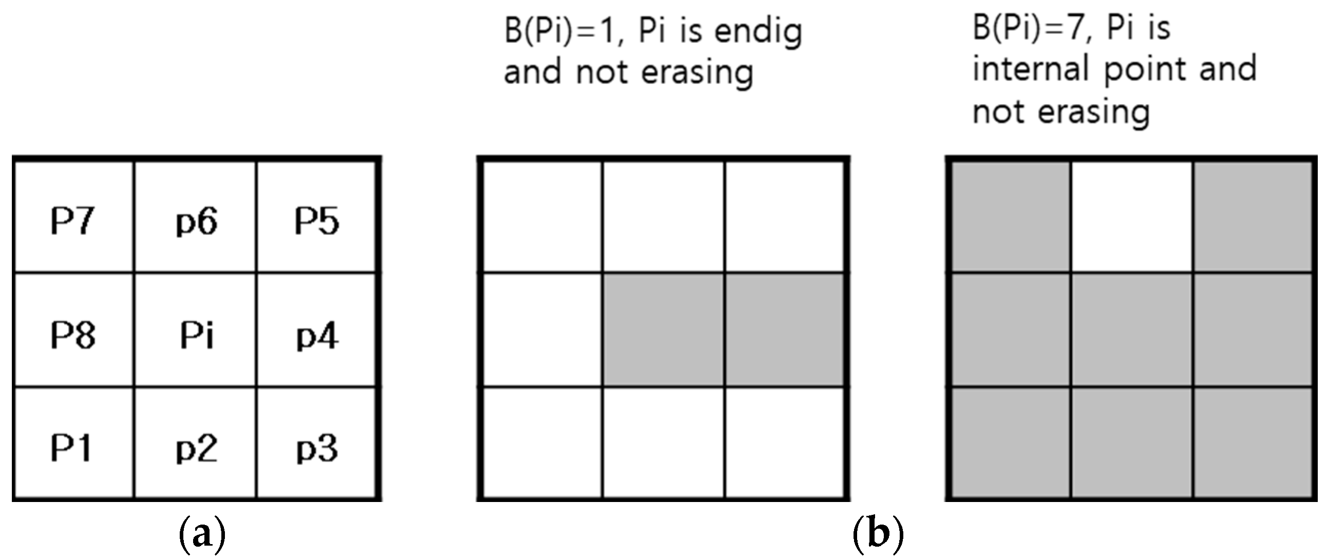
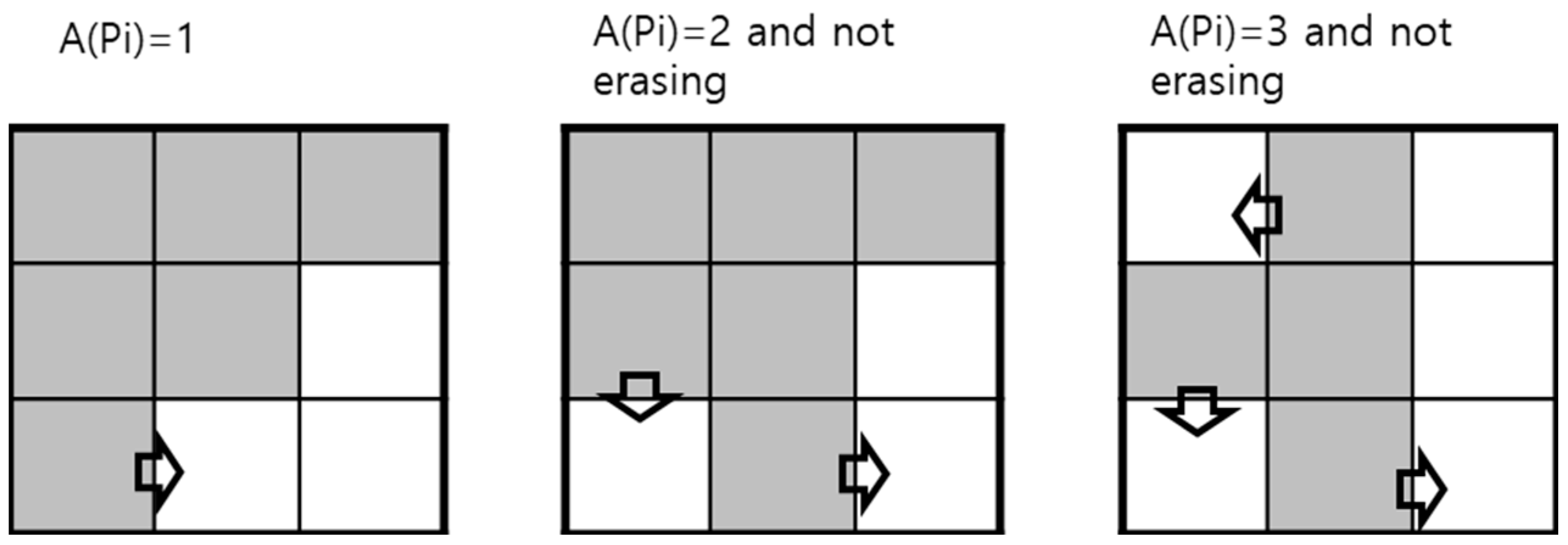
The thinning algorithm has long been used for pattern recognition and image analysis to extract feature points from images. Reduce the thick image to a binary digital pattern to obtain a unit width skeleton that retains its unique topology and geometric properties. The thinning process is to make the ridge a single line in the binarized image obtained by the Gabor filter. The best proven thinning algorithm is Zhang and Suen (ZS) in several algorithms [6,13,14]. The ZS algorithm performs two iteration steps in a 3 × 3 mask window. P(n) and P1 to 8 are the binary image values in Figure 7a. In this study, an image value of 0 means white and 1 means black. Thinning is only done when the center image Pi is black.
In the first sub iteration, the contour point Pi is deleted from the digital pattern if the following conditions are met: In the first step, the following conditions are evaluated for the central point Pi. When satisfied, the midpoint Pi turns white.
(i)
P(i) is a value between 2 and 6;
(ii)
A (Pi) = 1;
(iii)
At least one of P2 and P6 and P8 is 0;
(iv)
At least one of P4 and P6 and P8 is 0.
A(Pi) is the number of 01 patterns in Pi’s eight neighbors P1, P3, P4, …, P8 (Figure 8), and B(Pi) is the number of nonzero neighbors of P1, that is
B ( Pi )   =   N = 1 8 P n
As in the example in Figure 8, A (Pi) is 2 or 3. Since it is not 1, the Pi is not deleted. Where B(Pi) is the number of 1s in the neighboring pixels in Figure 7b.
In the second step only conditions (iii) and (iv) are changed. The image of the result of the first step is executed again under the following conditions.
(v)
At least one of P2 and P4 and P8 is 0;
(vi)
At least one of P2 and P4 and P6 is 0.
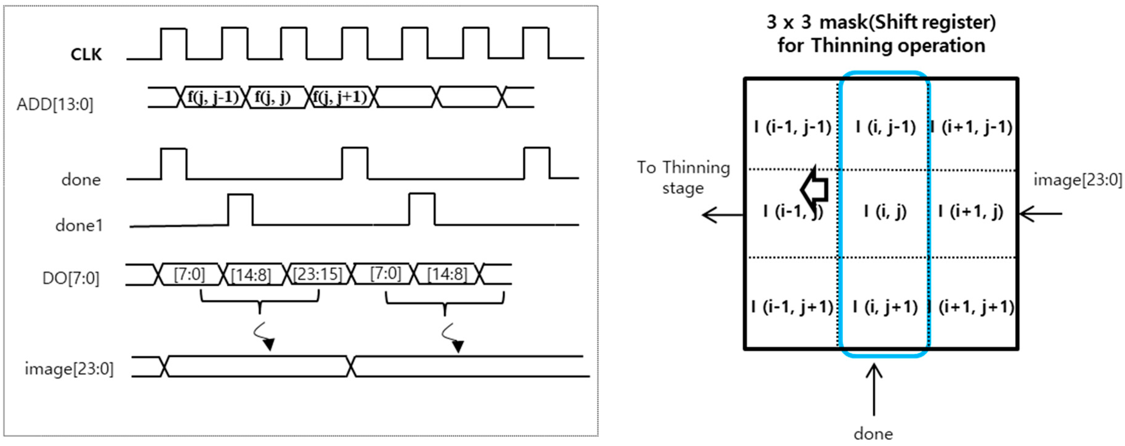
In this paper, we proposed the operation structure shown in Figure 9 for efficient operation of the ZS algorithm. The designed circuit generates an address of memory that matched with three vertical images. That is, every three clocks, an image of three pixels is transferred to the 3 × 3 2D shift register and simultaneously shifted to the left of the window. As shown in Figure 8, A(Pi) means the number of 1 to 0 (1 → 0) patterns in eight-neighbor pixels. In order to determine the coincidence of two consecutive P(n), P(n + 1) and 2 bit binary “10”, the circuit uses exclusive-OR operation and then not-OR. Add up all the values. In the case of this operation, it is possible to obtain a result faster than the previous SW operation because it is possible for one clock. The following Verilog-HDL code is applied to calculate the A[Pi] so that the value can be obtained within one clock by simple operation.
A(Pi) <= ~|({P1,P2} ^ 2′b10) + ~|({ P2,P3} ^ 2′b10) + ~|({ P3,P4} ^ 2′b10) + ~|({ P4,P5} ^ 2′b10) + ~|({ P5,P6} ^ 2′b10) + ~|({ P6,P7} ^ 2′b10) + ~|({ P7,P8} ^ 2′b10) + ~|({ P8,P1} ^ 2′b10) ;
It is possible to obtain a thinning result of Pi image in three clocks with simple circuit. The 24-bit image read from memory by three clocks is stored in the shift register by the ‘done’ signal, and 3 × 3 values and thinning operation is done, as shown in Figure 9.

4.3. Algorithm Processor Design

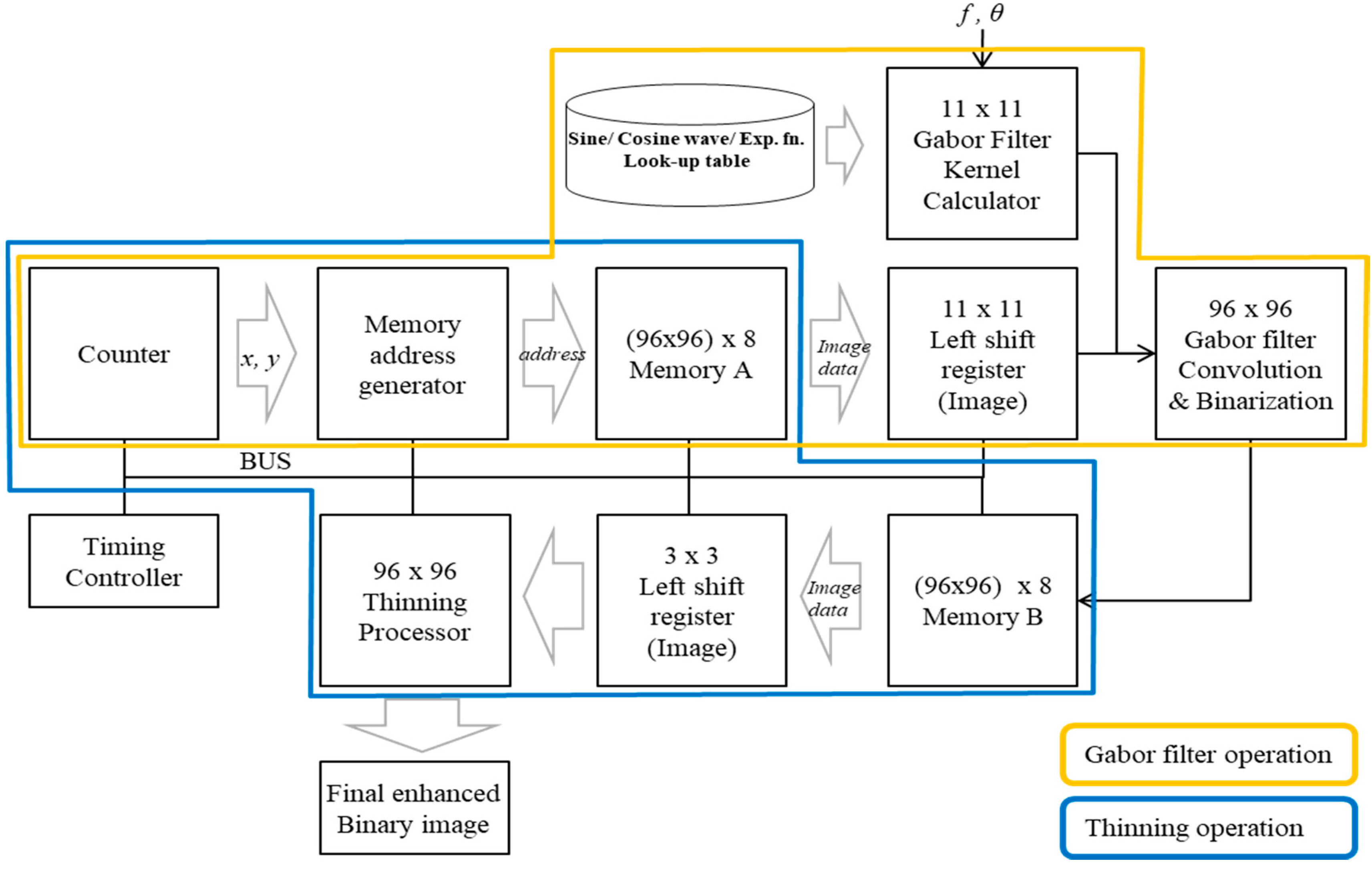
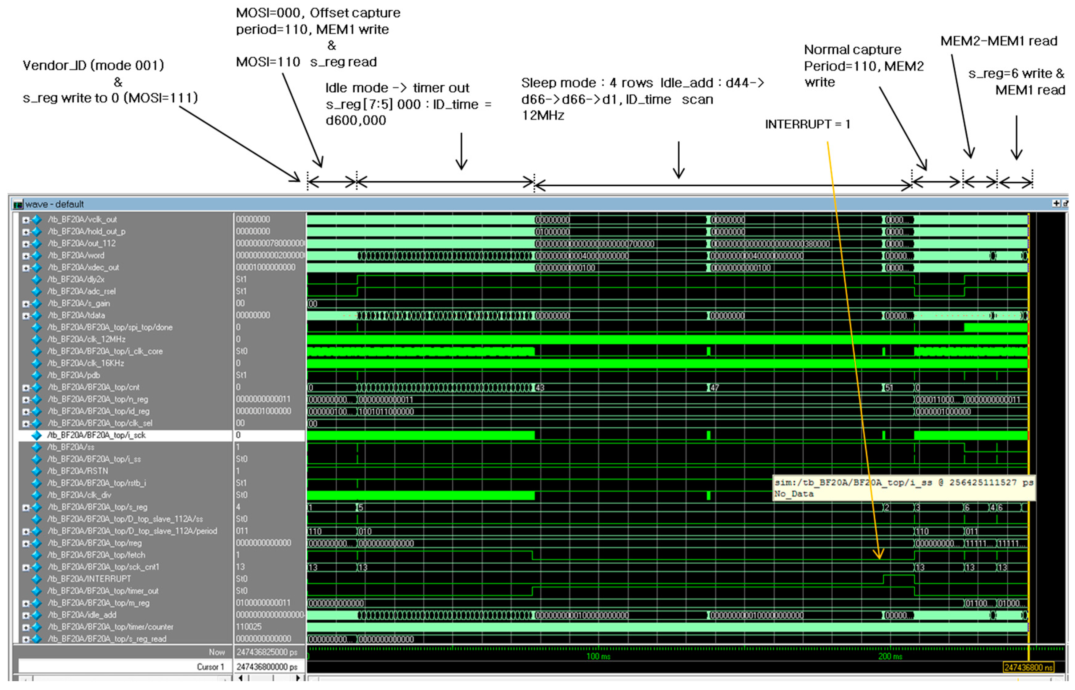
Figure 10 shows the integrated logic of proposed algorithm processor. The yellow box is Gabor filter block and blue box is thinning block. The address generator, counter and memory-A are shared. The logic was designed in RTL and synthesized by Synopsys Design Compiler using a 180n CMOS process. The Figure 11 shows the logic circuit simulation. Simultaneous operation is impossible because thinning must be processed with the image obtained as a result of Gabor filter. It took 266,439 cycles for Gabor filter operation and 55,303 cycles for thinning operation. The total required cycle is 321,742. The result shows a valid operation of proposed logic circuit. The layout is performed by auto P&R for the algorithm processor. The area is 0.962 mm2 and gate count is 96,393.

4.4. 16-Bit Risc MCU Design

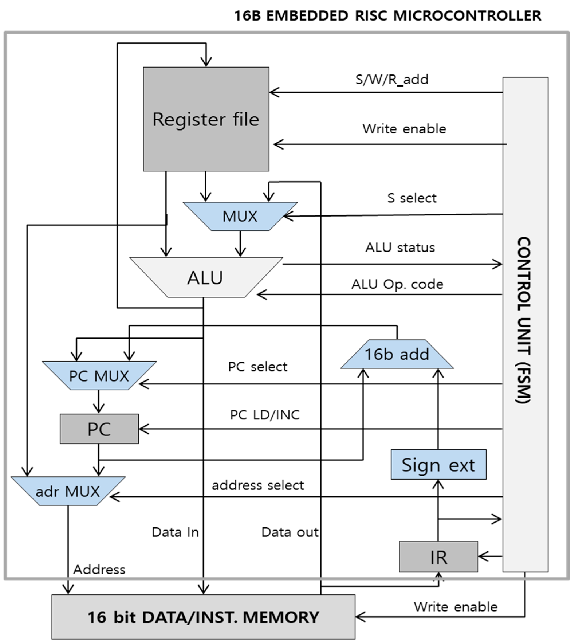
The 16-bit Reduced Instruction Set Computing (RISC) processor is designed using the Verilog harware description language (HDL), as shown in Figure 12. The processor handles the reset of the algorithm, except for Gabor and thinning. The processor has a four-stage pipeline. The applied embedded MCU is based on Harvard architecture with separate data memory and instruction memory to avoid bottlenecks and enable pipelines. Memory Access Instructions are Load and Store. Data Processing has eight instructions including arithmetic, logical and transfer operations. Control Flow Instructions are a branch on Equal, branch on not Equal and Jump. The basic architecture of a RISC processor is as given below. It includes eight general-purpose registers that can store 16-bit data and a 16-bit ALU that can perform logical and arithmetic operations. The flag register can check parity, carry, and zero status. Addressing Modes are Immediate, Register, Register Indirect and PC relative. The address for conditional jump instructions is calculated by adding the 16-bit sign-extension of an eight-bit signed offset to the program counter. The architecture was verified by Verilog with RTL and then synthesized at the Gate level using 180n CMOS design kit. The synthesized gate-level MCU first verified basic command operation in the FPGA environment. In the emulation environment, the number of cycles required for the rest of the algorithm except Gabor filter and thinning was analyzed. After the layout was performed with the Auto P&R tool, the back-annotation verification result was confirmed through post simulation. The layout area is 54,483 μm2 and gate count is 5460. The operating speed was maximum 50 MHz. It has been confirmed that the embedded 16-bit RISC core successfully performs steps excluding thinning and GB steps in the fingerprint authentication algorithm step.

5. Full Chip Integration

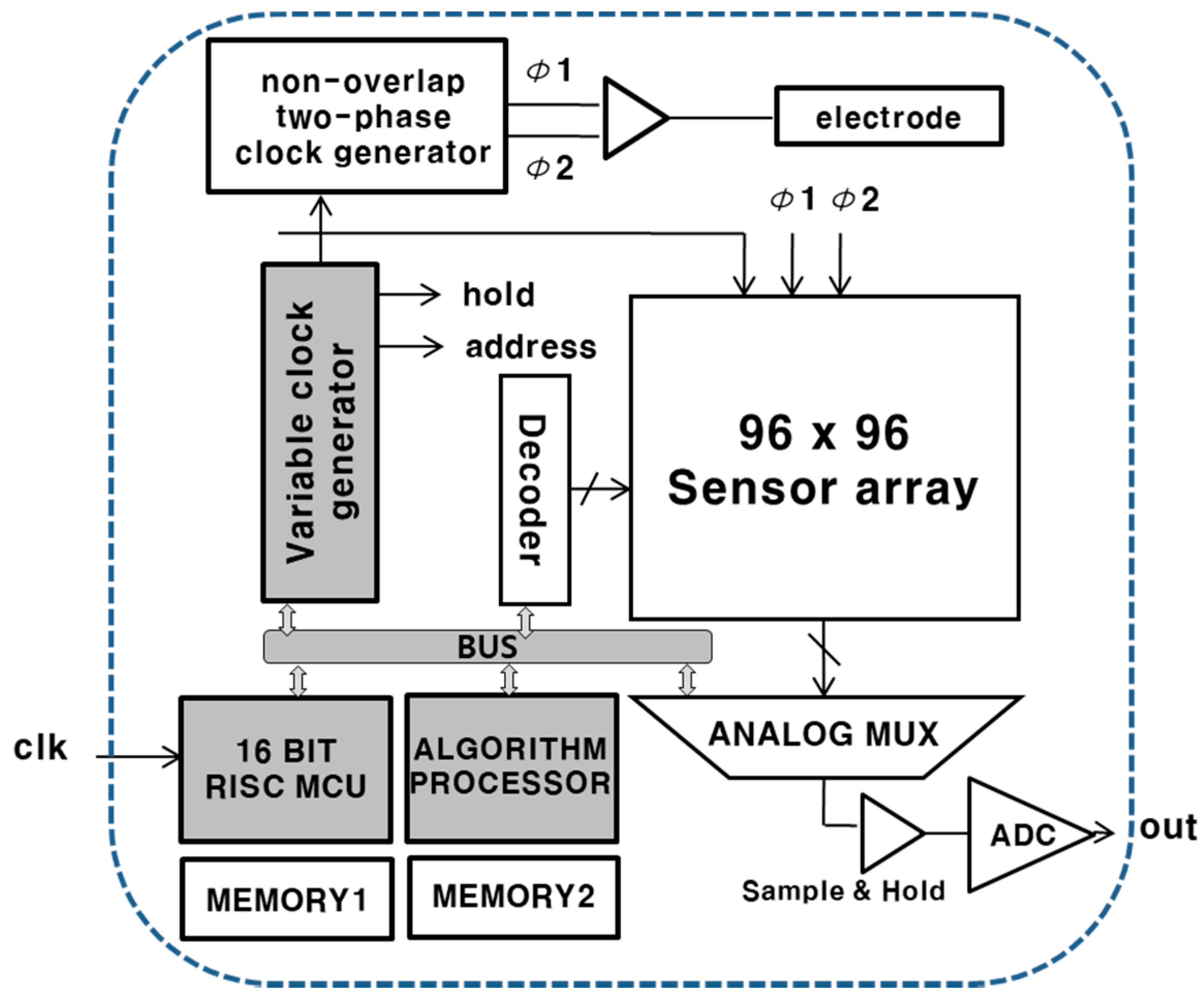
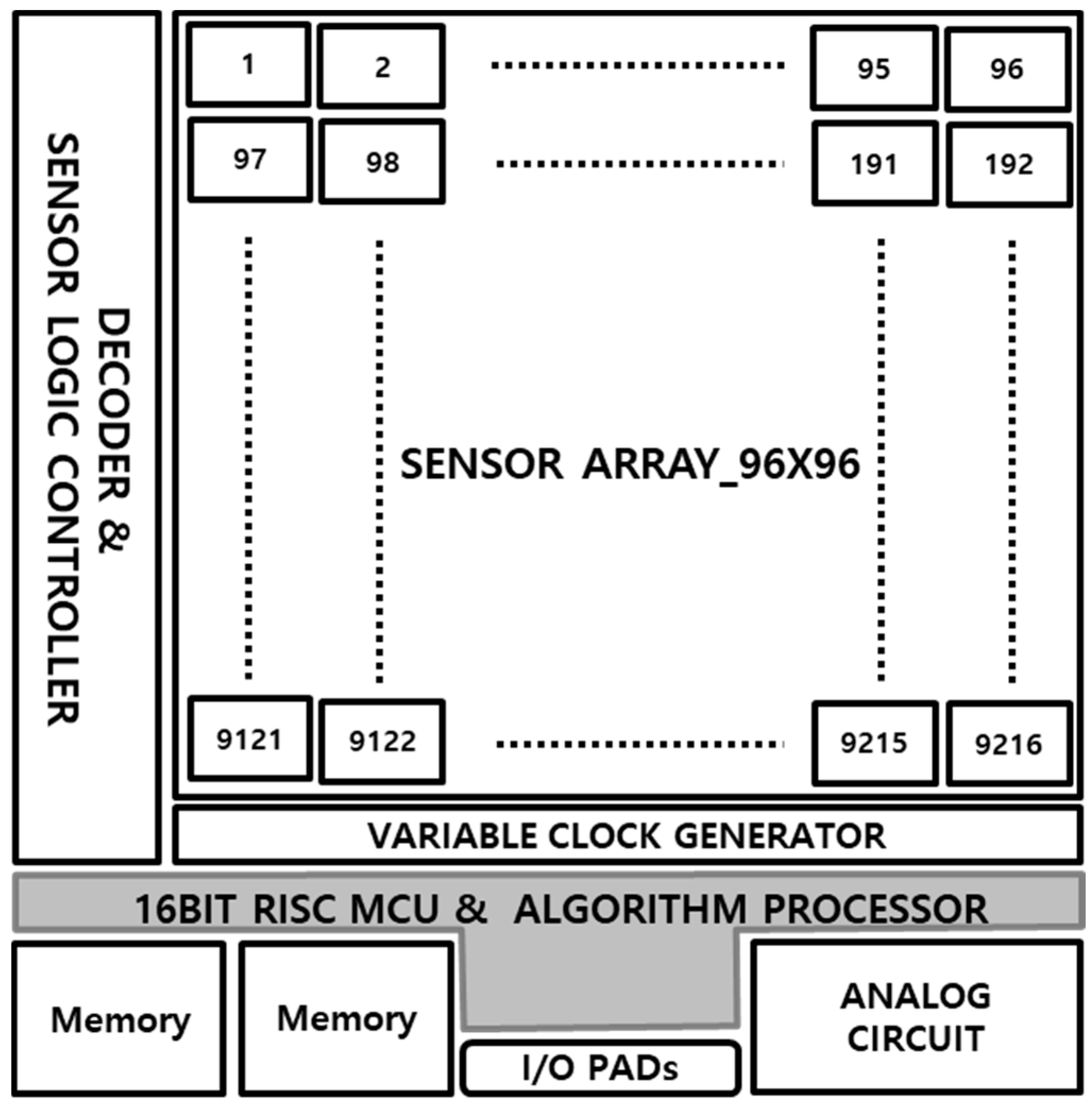
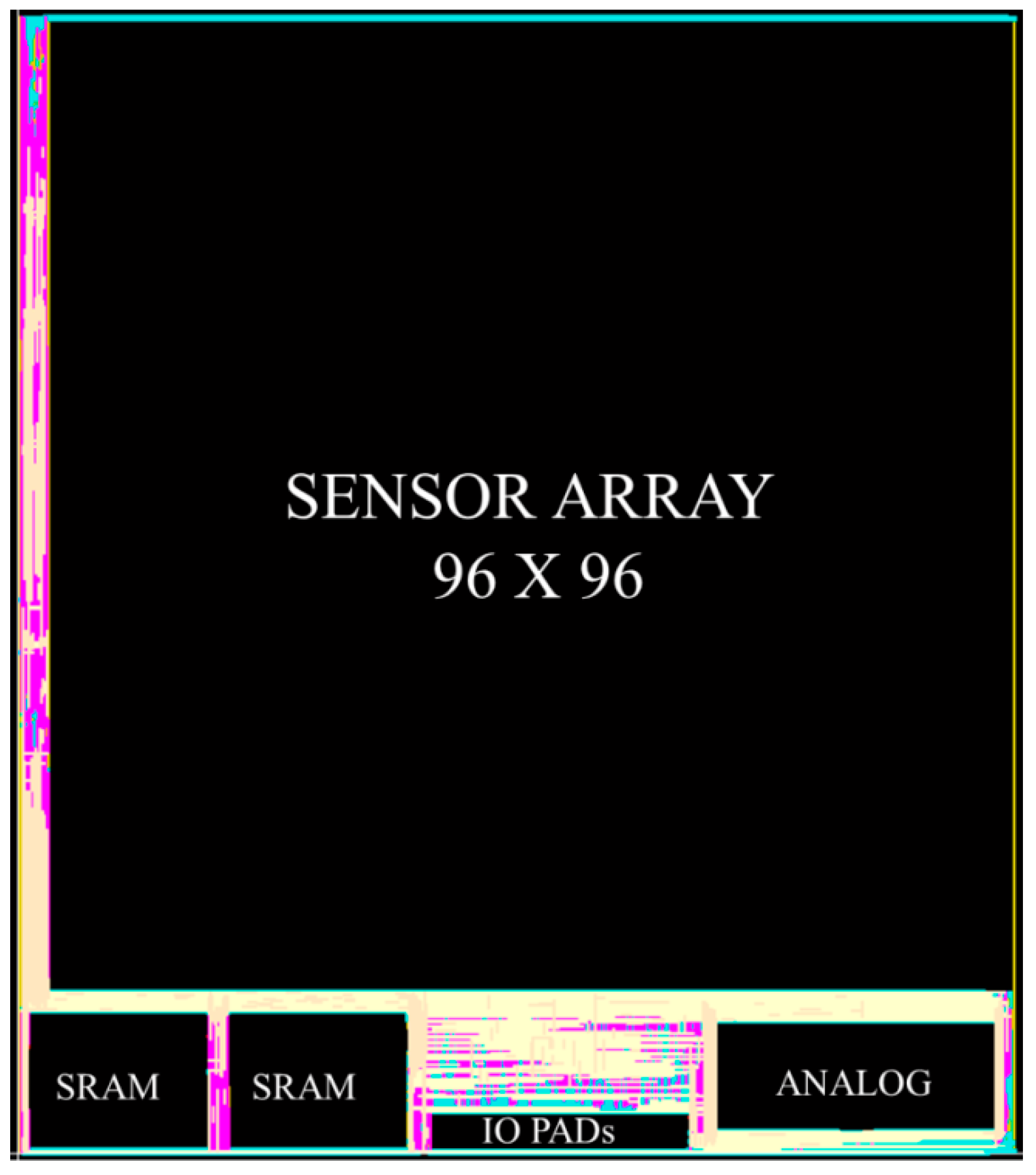
Figure 13 shows the functional block diagram and Figure 14 is floor planning of 96 × 96 fingerprint sensor chip. Figure 15 shows the logic simulation results of the single-chip architecture. Figure 16 shows the chip layout is 5010 μm × 5710 μm at 0.18 μm standard CMOS process. Since the sensor is an analog circuit, the design and layout are performed in a full custom method, and the entire chip is performed through automatic placement and routing in a cell-based design method. The circuit contains two compiled static memories, an input/output pad, and an analog block containing an ADC. Figure 17 shows the layout of the proposed single-chip fingerprint sensor scheme. The chip area is 28.61 mm2 and gate count is 2,866,700 with memory. To verify the behavior of the proposed processor, we extracted each parasitic capacitance from the layout and performed post-simulation with 180n CMOS conditions, as shown in Figure 15. This shows that the proposed method can effectively handle the fingerprint algorithm. The conventional fingerprint sensor does not include an algorithm processor and MCU. The area of an algorithm processor and MCU is 1.47 mm2. Therefore, the area of a conventional fingerprint sensor is 27.14 mm2. This means that the chip area increase in the proposed circuit is just 5.4%.
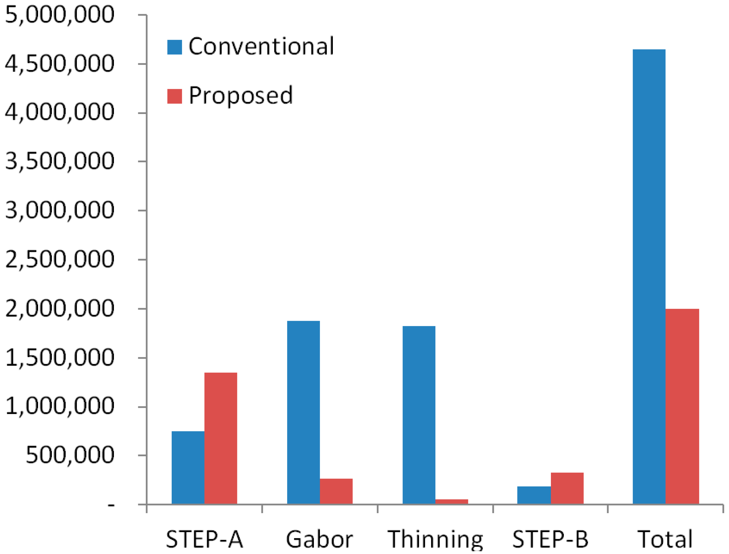
Table 2 compares the CPU occupancy of the conventional architecture and the proposed architecture. SETP-A means the algorithm before the GABOR filter, and STEP-B means the algorithm after THINNING. Figure 17 shows Table 2 as a graph, and shows that the proposed architecture shows 57% performance improvement in CPU cycle occupancy. Table 3 is a performance comparison considering the burden of increasing the chip area. Table 3 shows that even with a small area increase of 5.4% compared to the conventional chip, the proposed architecture can achieve 57% improvement in algorithm processing. It is a future work to analyze the improvement in power consumption through power analysis of the conventional circuit in the future. If the proposed architecture is embedded in the authentication fingerprint sensor system, it is expected to reduce the CPU burden and greatly improve the processing speed without significantly affecting the chip size.

6. Conclusions

This paper proposes a novel fingerprint sensor architecture that processes a binarization and thinning step, which occupy 80% of the algorithm processing time, in hardware, and the remaining steps, which is processed by embedded 16-bit RISC MCU. The CPU occupancy of the algorithm was analyzed using the ARM emulator and the FPGA environment. The algorithm processor was designed by applying the Gabor filter for a binarization and the ZS algorithm for a thinning. The rest of the algorithm is processed by an embedded 16-bit MCU with small circuit volume, so all steps of the algorithm can be processed on a single chip without an external CPU. In this paper, we implemented a 96 × 96 array high-sensitivity fingerprint sensor. In the sensor circuit of the pixel unit, an insensitive charge transfer integrator is applied that can effectively reduce the effect of parasitic capacitance. The proposed circuit in the paper uses an active output voltage feedback integrator. The whole circuit was verified by RTL simulation of digital blocks synthesized in a 180n two-poly six-metal standard process. The layout is performed by auto P & R for the full chip with 96 × 96 pixel array. The area of our chip is 5010 × 5710 μm (28.61 mm2) and the gate count is 2,866,700. The result is compared with a conventional one. The proposed scheme can reduce the algorithm processing time by 57% in total algorithm. If the designed architecture is adopted in the fingerprint AFIS, it is expected to reduce the CPU burden and greatly improve the processing speed without significantly affecting the chip size. Although not shown in the results of this paper, it is expected to reduce power consumption by minimizing the operation of the CPU implemented in a large-scale circuit. The addition of circuits for part of the algorithm leads to an increase in the chip area, but the proposed architecture has a relatively small burden on the chip area in terms of speed improvement. The proposed architecture improves the algorithm speed by up to 57%, so we can replace the traditional 64-bit or 32-bit CPU with a 16-bit or 8-bit CPU, which will enable low power consumption and the implementation of small fingerprint systems.

Funding

This research received no external funding

Acknowledgments

This work was supported by Hanshin University Research Grant.

Conflicts of Interest

The authors declare no conflict of interest.

References

  1. Chugh, T.; Cao, K.; Jain, A.K. Fingerprint spoof buster: Use of minutiae-centered patches. IEEE Trans. Inf. Forensics Secur. 2018, 13, 2190–2202. [Google Scholar] [CrossRef]
  2. Tolosana, R.; Gomez-Barrero, M.; Busch, C.; Ortega-Garcia, J. Biometric presentation attack detection: Beyond the visible spectrum. IEEE Trans. Inf. Forensics Secur. 2019, 15, 1261–1275. [Google Scholar] [CrossRef] [Green Version]
  3. Jung, S.-M.; Nam, J.-M.; Yang, D.-H.; Lee, M.-K. A CMOS integrated capacitive fingerprint sensor with 32-bit RISC microcontroller. IEEE J. Solid-State Circuits 2005, 40, 1745–1750. [Google Scholar] [CrossRef]
  4. Alibeigi, E.; Samavi, S.; Shirani, S.; Rahmani, Z. Real time ridge orientation estimation for fingerprint images. Computer Vision and Pattern Recognition. arXiv 2017, arXiv:1710.05027. [Google Scholar]
  5. Gayathri, S.; Sridhar, V. Design and simulation of Gabor filter using verilog HDL. Int. J. Latest Trends Eng. Technol. 2013, 2, 77–83. [Google Scholar]
  6. Chen, W.; Sui, L.; Xu, Z.; Lang, Y. Improved Zhang-Suen thinning algorithm in binary line drawing applications. In Proceedings of the 2012 International Conference on Systems and Informatics (ICSAI2012), Yantai, China, 19–20 May 2012; pp. 1947–1950. [Google Scholar]
  7. Voß, N.; Mertsching, B. Design and Implementation of an Accelerated Gabor Filter Bank Using Parallel Hardware. In International Conference on Field Programmable Logic and Applications; Springer: Berlin/Heidelberg, Germany, 2001; pp. 451–460. [Google Scholar]
  8. Spinei, A.; Pellelin, D.; Fernandes, D.; Heraults, J. Fast Hardware Implementation of Gabor Filter Based Motion Estimation. Integr. Comput. Eng. 2000, 7, 67–77. [Google Scholar] [CrossRef] [Green Version]
  9. Painkras, E.; Charoensak, C. A VLSI architecture for Gabor filtering in face processing applications. In Proceedings of the 2005 International Symposium on Intelligent Signal Processing and Communication Systems, Hong Kong, China, 13–16 December 2005. [Google Scholar]
  10. Jothi, S.A.; Dhatchayani, K.; Devi, G.G.R.; Raja, M.R. VLSI Implementation of Gabor Filter in Image Detection–Research Direction. Int. J. Circuit Theory Appl. 2017, 10, 133–138. [Google Scholar]
  11. Kheiri, F.; Samavi, S.; Karimi, N. Hardware design for binarization and thinning of fingerprint images. arXiv 2017, arXiv:1710.05749. [Google Scholar]
  12. Das, R.K.; De, A.; Pal, C.; Chakrabarti, A. DSP hardware design for fingerprint binarization and thinning on FPGA. In Proceedings of the 2014 International Conference on Control, Instrumentation, Energy and Communication (CIEC), Calcutta, India, 31 January–2 February 2014. [Google Scholar]
  13. Wakil, Y.; Tariq, S.G.; Humayun, A.; Abbas, N. An FPGA based Minutiae Extraction System for Fingerprint Recognition. Int. J. Comput. Appl. 2015, 111, 31–35. [Google Scholar] [CrossRef]
  14. Hermanto, L.; Sudiro, S.A.; Wibowo, E.P. Hardware implementation of fingerprint image thinning algorithm in FPGA device. In Proceedings of the 2010 International Conference on Networking and Information Technology, Manila, Philippines, 11–12 June 2010. [Google Scholar]
  15. SUPREMA. Available online: https://www.supremainc.com/embedded-modules/en/main.asp (accessed on 28 August 2020).
  16. Jung, S. Implementation of 144 × 64 Pixel Array Bezel-Less CMOS Fingerprint Sensor. Int. J. Smart Sens. Intell. Syst. 2018, 11, 1–5. [Google Scholar] [CrossRef] [Green Version]
  17. Jung, S. A Modified Architecture for Fingerprint Sensor of Switched Capacitive Integrator Scheme. Int. J. Bio-Sci. Bio-Technol. 2016, 8, 139–144. [Google Scholar] [CrossRef]
  18. Yeo, H. Analysis and Performance Comparison of Charge Transfer Circuits for Capacitive Sensing. J. Next Gener. Inf. Technol. 2014, 5, 16–26. [Google Scholar]
  19. Hyeopgoo, Y. A New Fingerprint Sensor based on Signal Integration Scheme using Charge Transfer Circuit. Int. J. Bio-Sci. Bio-Technol. 2015, 7, 29–38. [Google Scholar] [CrossRef] [Green Version]
  20. Yeo, H. Touch fingerprint sensor based on sensor cell isolation technique with pseudo direct signalling. Int. J. Smart Sens. Intell. Syst. 2019, 12, 1–9. [Google Scholar]
  21. Hong, L.; Wan, Y.; Jain, A. Fingerprint Image Enhancement: Algorithm and Performance Evaluation. IEEE Trans. Pattern Anal. Mach. Intell. 1998, 20, 777–789. [Google Scholar] [CrossRef] [Green Version]
  22. Molaei, S.; Abadi, M.E.S.A. Maintaining filter structure: A Gabor-based convolutional neural network for image analysis. Appl. Soft Comput. 2020. [Google Scholar] [CrossRef]
  23. Jung, S. Design of low power and high speed CMOS fingerprint sensor Design of low power and high speed CMOS fingerprint sensor. Int. J. Bio-Sci. Bio-Technol. 2013, 5, 1–16. [Google Scholar]
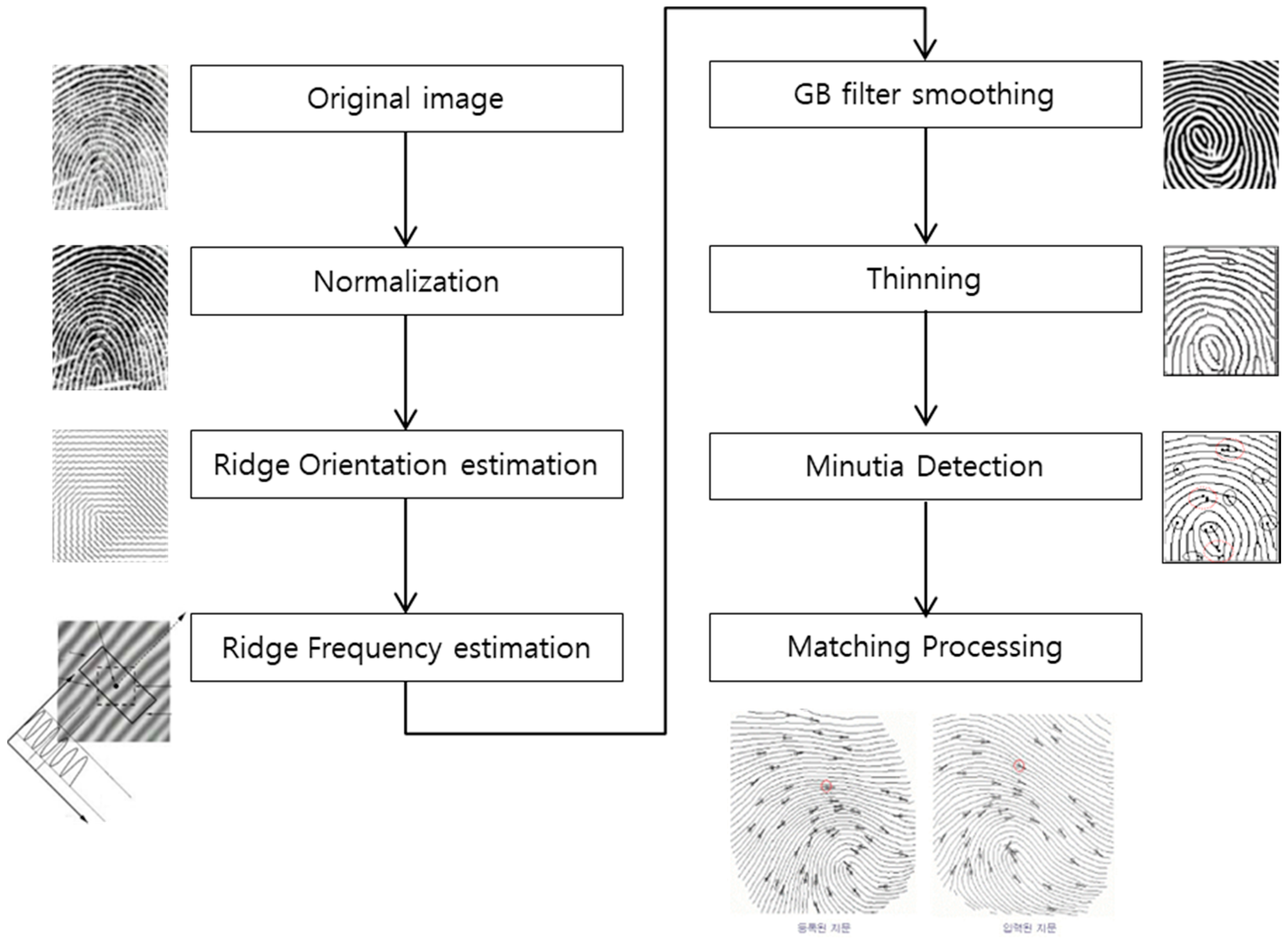
Figure 1. Fingerprint identification algorithm.
Jsan 09 00051 g001
Figure 2. Pixel-level Sensor scheme and output voltage.
Jsan 09 00051 g002
Figure 3. Pipelined scan driver architecture with variable clock generator.
Jsan 09 00051 g003
Figure 4. FPGA emulation board for verifying the algorithm.
Jsan 09 00051 g004
Figure 5. 2D Gabor wavelet and example of 5-frequency, 8-orientation 40 filter bank.
Jsan 09 00051 g005
Figure 6. Gabor filter convolution using 11 × 11 shift register.
Jsan 09 00051 g006
Figure 7. pixel order and sample of N(Pi). (a) 3 × 3 winow index (b) number of black pixel neighbor P(i).
Jsan 09 00051 g007
Figure 8. Number of black to white change around P(i).
Jsan 09 00051 g008
Figure 9. Thinning operation using 3 × 3 shift register.
Jsan 09 00051 g009
Figure 10. Functional block diagram of algorithm processor.
Jsan 09 00051 g010
Figure 11. Algorithm processor simulation results.
Jsan 09 00051 g011
Figure 12. Functional block diagram of proposed 16-bit RISC MCU.
Jsan 09 00051 g012
Figure 13. Logic diagram of fingerprint sensor chip.
Jsan 09 00051 g013
Figure 14. Floorplan of fingerprint sensor chip.
Jsan 09 00051 g014
Figure 15. Post-simulation result of full chip.
Jsan 09 00051 g015
Figure 16. Layout of proposed architecture (5010 × 5710 μm2 @180n 2-poly 6-metal CMOS process).
Jsan 09 00051 g016
Figure 17. Graph of CPU cycle distribution.
Jsan 09 00051 g017
Table 1. CPU cycle distribution of the algorithm in 96 × 96 pixel sample images.
Process StepInstruction Cycle
S-cycleN-cycleI-cycleTotal%
Normalization25,1686292314634,6060.75%
Orientation Estimation176,02347,70547,520271,2485.84%
Frequency Estimation307,42488,57750,706446,7069.62%
Gabor Filtering1,314,689329,066230,5021,874,25740.37%
Thinning983,279577,092265,9391,826,31039.34%
Minutiae Detection118,45340,74117,642176,8363.81%
Matching Processing11,54038981612,7460.27%
Total Clock2,936,5771,089,862616,2714,642,709100%
Table 2. Comparison of CPU cycle distribution.
STEP-AGaborThinningSTEP-BTotal
Conventional752,5601,874,2571,826,310189,5824,642,709
Proposed1,346,420266,43955,303330,4771,998,639
Table 3. Performance comparison between the proposed and previous method. (@180n CMOS process, 96 × 96 pixel array).
Conventional Architecture (SW only)Proposed Architecture ((SW+HW+MCU))Improvement (%)Remarks
Total CPU Cycle4,642,7091,998,63957
Chip Area (mm2) with 2 SRAM27.1428.61−5.496 × 96 pixels area full chip
Power Consumption-5.25 mW-20 MHz, 1.8 V
Publisher’s Note: MDPI stays neutral with regard to jurisdictional claims in published maps and institutional affiliations.