Article

A Design of Rectifier with High-Voltage Conversion Gain in 65 nm CMOS Technology for Indoor Light and RF Energy Harvesting

by
Jefferson Hora
1,*,
Gene Fe Palencia
1,
Rochelle Sabarillo
1,
Johnny Tugahan
1,
Yichuang Sun
2 and
Xi Zhu
3
1
Center for Integrated Circuits Design (CICD-Microlab), Mindanao State University-Iligan Institute of Technology, Iligan City 9200, Philippines
2
School of Physics, Engineering and Computer Science, University of Hertfordshire, Hatfield AL10 9AB, Hertfordshire, UK
3
School of Electrical and Data Engineering, University of Technology Sydney, Sydney, NSW 2007, Australia
*
Author to whom correspondence should be addressed.
J. Sens. Actuator Netw. 2025, 14(6), 117; https://doi.org/10.3390/jsan14060117
Submission received: 19 October 2025 / Revised: 30 November 2025 / Accepted: 2 December 2025 / Published: 11 December 2025

Abstract

In rectifier design, the key parameters are the voltage–conversion ratio and the power conversion efficiency. A new circuit design approach is presented in which a capacitor-based, cross-coupled, differential-driven topology is used to boost the voltage–conversion ratio. The scheme also integrates an auxiliary current path to raise the power conversion efficiency. To demonstrate its practicality, two three-stage rectifiers were designed and fabricated using standard 65 nm CMOS technology. The designs were tested under various conditions to assess their performance. The first rectifier targets indoor light energy harvesting applications. It achieves a peak voltage conversion ratio of 3.94 and a maximum power conversion efficiency of 58.7% when driving a 600 Ω load, while supplying over 2 mA of output current. The second rectifier is optimized for RF energy harvesting at 2.4 GHz. Experimental results indicate that it can deliver 70 µA to a 50 kΩ load, with a peak voltage conversion ratio of 5 and a power conversion efficiency of 17.5%.

1. Introduction

Over the past two decades, wireless sensor networks (WSNs) have evolved rapidly, and their integration into the Internet of Things (IoT) has expanded their potential applications in smart manufacturing, smart grids, and intelligent surveillance systems [1,2,3]. These systems rely on a large number of sensor nodes, many of which must operate in remote or inaccessible locations. Ensuring long-term autonomous operation, therefore, requires methods of harvesting energy from the surrounding environment, minimizing the need for wired power or battery replacements.
Various energy harvesting (EH) techniques have been developed, such as indoor light harvesting using photovoltaic (PV) cells [4,5], RF energy scavenging [6,7,8], thermoelectric generation [9], and piezoelectric conversion [10]. Among these, PV and RF energy sources are particularly suitable for indoor operation, providing complementary functionality for continuous energy availability [11,12]. In this work, both sources are integrated in a hybrid EH system, as illustrated in Figure 1. A custom-designed DC-to-pulsating-signal converter enables the PV output to share the same rectifier used for RF input, avoiding the need for bulky off-chip inductors or control circuits [13,14]. The rectified DC power is stored in an energy reservoir (battery or supercapacitor) that supplies key WSN subsystems such as the MCU and transceiver.
The rectifier circuit is the critical block determining the efficiency of the entire EH system. Conventional CMOS rectifiers, however, suffer from several inherent limitations:
(1) Threshold voltage drops across transistors reduce the achievable output voltage and voltage conversion ratio (VCR); (2) leakage and parasitic capacitances lower the power conversion efficiency (PCE); and (3) device mismatch and non-symmetric charge transfer cause efficiency degradation at low input power levels. Cross-coupled differential structures partially mitigate these issues by enhancing gate drive, yet their PCE remains limited under weak input signals and low supply conditions.
To overcome these challenges, this work proposes a capacitor-based, cross-coupled, differential-drive (CCDD) rectifier incorporating an auxiliary PMOS-diode path. The split coupling capacitor increases voltage boosting capability, while the auxiliary conduction path improves charge transfer efficiency and compensates for threshold losses. This com- combination achieves both higher VCR and PCE under low input amplitude, making it well-suited for compact and energy-constrained IoT sensor nodes.
The remainder of this paper is organized as follows: Section 2 reviews related rectifier topologies. Section 2.1, Section 2.2, Section 2.3, Section 2.4 and Section 2.5 detail the proposed CCDD rectifier and its auxiliary enhancement path. Section 3 presents measurement results and comparisons, and Section 4 concludes the work.

2. Materials and Methods

2.1. Definitions and Notation

Throughout this work, the input signal amplitude VIN refers to the peak value of the sinusoidal waveform. When input power is expressed in decibels relative to one milliwatt (dBm) for a 50 Ω system, the corresponding peak and peak-to-peak voltages can be obtained as
V R M S = P I N × R ,   V P = 2 P I N × R ,   V P P = 2 2 P I N × R
where PIN is the input power in watts and R = 50 Ω. For example, PIN = 0 dBm (1 mW) corresponds to VPP = 0.632 V across a 50 Ω source.
All simulated and measured waveforms presented in this paper adopt this voltage convention. PCE is defined as
P C E = P O U T , D C P I N , A C
where POUT,DC is the output DC power delivered to the load, and PIN,AC is the RF power delivered at the rectifier input after de-embedding probe and cable losses. Table 1 provides the list of symbols and abbreviations adopted throughout this work.

2.2. Rectifier Architecture and Operation

In the hybrid energy harvesting system discussed earlier, the rectifier plays a central role in converting the low-level AC or pulsating signal from the PV and RF sources into a stable DC output. The performance of the entire energy harvesting module, therefore, depends critically on the rectifier’s ability to achieve high VCR and PCE under low input amplitude. Designing such a circuit requires balancing multiple trade-offs, including device sizing, leakage reduction, and voltage boosting capability. To provide a foundation for the proposed design, this section first reviews conventional CMOS rectifier structures, discusses their limitations, and then introduces the improved CCDD rectifier with an auxiliary PMOS path.
CMOS rectifiers rely on transistors that act as switches to turn the AC input into DC. In EH applications, the input signal is weak, so a single-stage rectifier cannot reach the voltage needed to charge a battery. Designers therefore employ multi-stage rectifiers to raise the output voltage. This approach, however, creates a trade-off: increasing voltage often lowers PCE. A higher output voltage can be obtained only by reducing the forward voltage drop VDROP [15,16], which equals the peak output current ID multiplied by the on-state resistance RDS_ON of each transistor.
To reduce RDS_ON, larger transistors are typically preferred. However, increasing transistor size adversely affects PCE, as it lowers the OFF-state resistance, thereby increasing reverse leakage current [17,18]. This trade-off complicates the design process, since optimizing both output voltage and efficiency simultaneously is challenging. Consequently, developing rectifier circuits that can deliver high output voltage while maintaining high PCE requires innovative and carefully balanced design strategies.
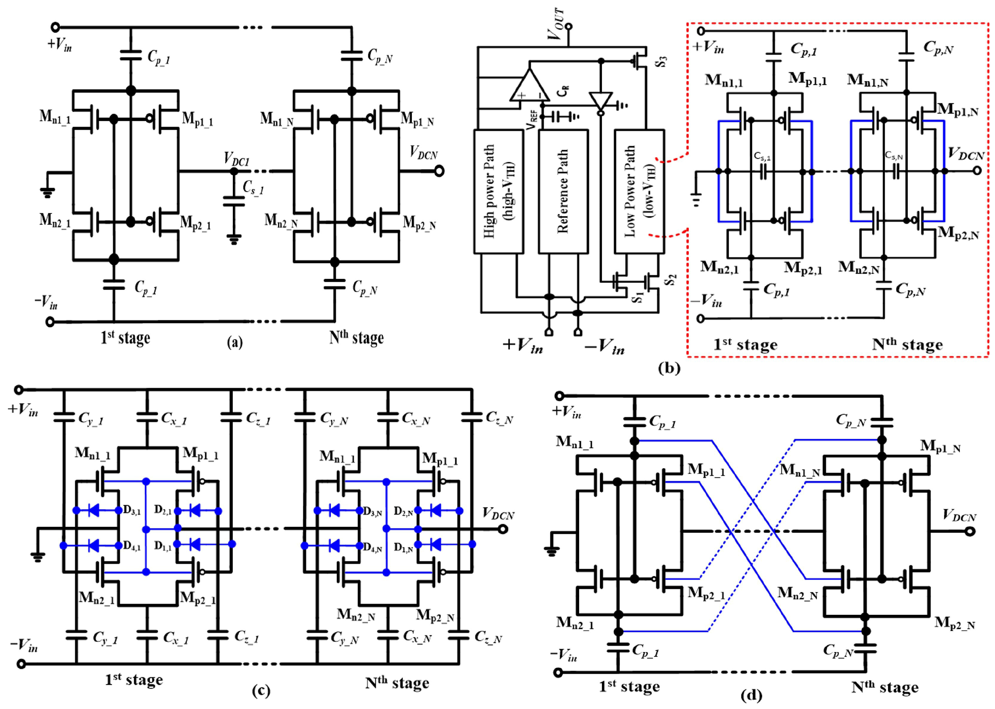
The dependence of the forward voltage drop VDROP on the threshold voltage VTH has prompted numerous threshold-cancelation schemes [19,20,21,22,23,24]. A widely adopted approach is the capacitor-based, cross-coupled, differential-drive (CCDD) structure [16,17,23,25], which effectively reduces the negative impact of VTH on both VCR and PCE. Among these techniques, the CCDD architecture has become a standard design, illustrated in Figure 2a [23].
Parallel efforts to enhance rectifier performance have led to several innovative schemes. One design [26], shown in Figure 2b, employs dual-current paths combining low- and high-VTH transistors to improve sensitivity and PCE. Another approach [17], shown in Figure 2c, uses a self-biased structure with feedback through diode-connected transistors to suppress reverse leakage while preserving efficiency. Figure 2d depicts the dynamic threshold control method in [25], which modulates the bulk voltage to vary VTH dynamically, further enhancing sensitivity and efficiency.
The preceding discussion shows that most recent work focuses primarily on improving PCE, while relatively few studies address boosting output voltage, or equivalently, the VCR, which is crucial for efficient battery charging. Cascading multiple stages increases voltage but also adds parasitics and complexity. Therefore, an ideal rectifier should achieve high output voltage with as few stages as possible to maintain simplicity and high efficiency.

2.3. Analysis of Conventional CCDD Circuit Structure

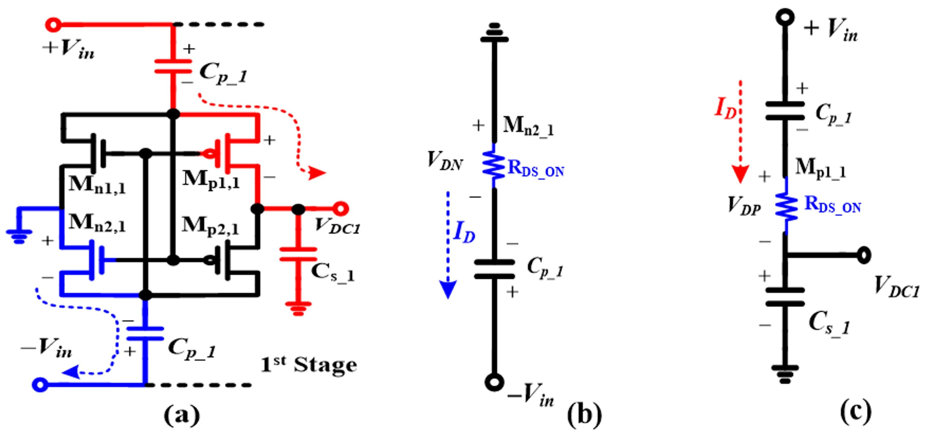
Earlier sections introduced the CCDD topology, one of the most widely used CMOS rectifier schemes. Figure 3 outlines its operation. The discussion that follows examines a single CCDD stage. In this circuit, pumping capacitors CP move charge in tandem with the NMOS and PMOS switches. Differential inputs, ±VIN, start the rectification process; VDN and VDP mark the drops across the NMOS and PMOS devices, respectively. The first stage produces a DC node VDC1 that is stored on capacitor CS1 and also feeds the next stage.
For clarity, the subsequent analysis considers only the forward-conduction losses of the NMOS and PMOS switches. Because the CCDD topology is symmetric and operates differentially, studying a single half-cycle is enough to extract the resulting DC output voltage.
In the first half-cycle, when |VIN| > VTH, the positive input (+VIN) switches on NMOS Mn2_1. The device then presents its on-state resistance RDS_ON, creating a low-impedance path for current to flow from ground toward −VIN. At the same moment, the negative input (−VIN) biases PMOS Mp1_1 into conduction, directing charge from +VIN through the pump capacitor CP1 into the storage capacitor CS1.
In the subsequent half-cycle, the roles of the transistors reverse: Mn1_1 and Mp2_1 conduct while Mn2_1 and Mp1_1 are turned off. By applying KVL during the charging phase, illustrated in Figure 3b, the corresponding voltage relationships and resulting equations for the expected DC output can be derived.
VinVcp_1 + VDN = 0
Rearranging Equation (3) gives the peak voltage Vcp_1 across the pumping capacitor Cp1, thus we obtain
Vcp_1 = −Vin + VDN
In the discharge half-cycle illustrated in Figure 3c, the peak input signal is given by
+Vin = Vcp_1 + VDP + VDC1
Substituting Equation (4) into Equation (5) yields the following expression for the output DC voltage of a single-stage rectifier,
VDC1 = 2Vin − (VDN + VDP)
The first stage’s rectified voltage, VDC1, serves as the input supply for the next stage. Because each stage uses the same circuit configuration, the overall DC output of a conventional N-stage CCDD rectifier can be estimated as
VDCN = N [2Vin − (VDN + VDP)]
As the analysis shows, the anticipated voltage-doubling effect is constrained by the cumulative forward voltage drop (VDROP = VDN + VDP) across the conducting NMOS and PMOS transistors. This drop negatively affects both VDC1 and the final output voltage VDCN. To achieve a higher output voltage, it is essential to minimize VDN and VDP as much as possible. However, while factors such as the load current (IL) and the transistor sizing (i.e., width-to-length ratio) can significantly influence the rectifier’s power-conversion efficiency, their impact on boosting the output voltage remains relatively limited [27,28]. Therefore, mitigating the effects of VDROP requires innovative circuit design strategies, as it cannot be addressed effectively through basic transistor sizing alone.

2.4. Study of the Capacitor-Based CCDD Rectifier Topology

Equation (5) implies that adding an auxiliary voltage Vaux can increase the rectifier’s output by compensating for the voltage drops in the last two terms. The resulting relationship is given by
VDCN = N [2Vin − (VDN + VDP) + Vaux]
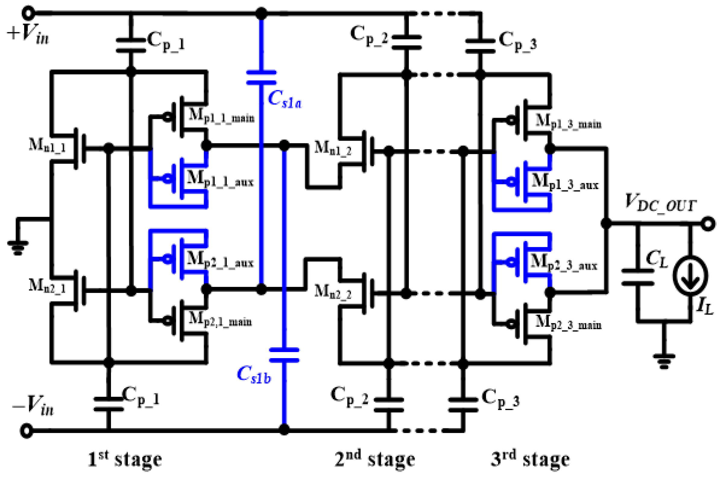
The Vaux in Equation (8) may be derived from on-chip circuitry or fed from an external source. To demonstrate the practical feasibility of this concept, a three-stage prototype rectifier was developed and is depicted schematically in Figure 4. To implement the Vaux term, two key modifications were introduced relative to the baseline CCDD architecture, both highlighted in blue within the schematic. The first enhancement involves adopting a capacitor-based CCDD structure, which facilitates voltage boosting by leveraging additional charge transfer paths.
In contrast to the conventional designs shown in Figure 2a and Figure 3, the storage capacitor CS, typically placed between the first and second stages, is divided into two separate capacitors, denoted as CS1a and CS1b. Furthermore, two PMOS transistors that are diode-connected are incorporated into the rectifier to counteract and mitigate the efficiency degradation introduced by the additional passive components. The theoretical analysis and operational impact of these two design modifications are discussed in detail in the following subsections.
Due to the differential topology, each split capacitor is set to one-half of the original CS_1 value and placed symmetrically, ensuring identical operation in both half-cycles. During the positive half-cycle, CS1b operates with Mp1 and Mn2; during the negative half-cycle, CS1a pairs with Mp2 and Mn1. Each split capacitor links the complementary input line to its corresponding complementary output node in the stage. As a result, during the discharging phase, the complementary input signal contributes additional voltage, effectively boosting the DC output.
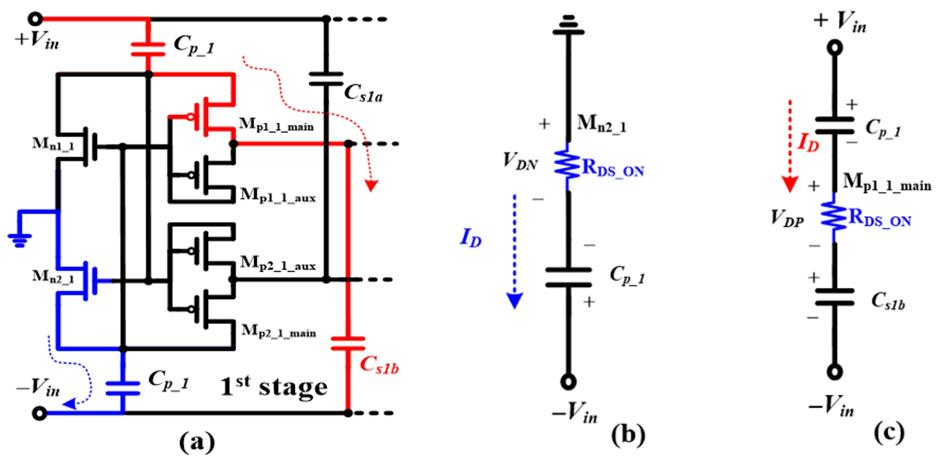
The steady-state charge and discharge behavior of this capacitor-enhanced CCDD rectifier is illustrated in Figure 5a and Figure 5b, respectively. Applying the analytical procedure used for the conventional CCDD rectifier shows that the charging phase follows the same expressions as Equations (3) and (4). However, analyzing the discharging cycle under this modified structure leads to an updated expression for the voltage across the pumping capacitor Vcp_1, given by
+Vin = Vcp_1 + VDP + VCs1bVin
Substituting Equation (4) into the modified discharge expression in Equation (9), the resulting voltage across the storage capacitor VCs1b can be expressed as
+Vin = −Vin + VDN + VDP + VCs1bVin
Rearranging Equation (10) yields the expression for the split storage capacitor Cs1b voltage in the proposed rectifier architecture,
VCs1b = 3Vin − (VDP + VDN)
With the input signal VIN reversed, the split-capacitor voltage VCs1a behaves identically to that given in Equation (11). It should be noted that the split-capacitor configuration is applied only between stages. As a result, each of these intermediate stages contributes roughly three times the input voltage, compared to two times per stage in the conventional design shown in Equation (7). However, in the final stage, the outputs are directly connected to the load without using split capacitors. This means the last stage contributes only twice the input voltage. With this combination of a differential structure in the intermediate stages and a standard output stage similar to the classical CCDD design, the total DC output voltage of an N-stage rectifier can still be reasonably estimated based on this mixed configuration and expressed as
VDCN_NEW = N [3Vin − (VDN + VDP)] − Vin
Equations (7) and (12) show that the proposed architecture gains an additional VIN per stage in the rectified output voltage.

2.5. Analysis of the Auxiliary Path Designed to Boost PCE

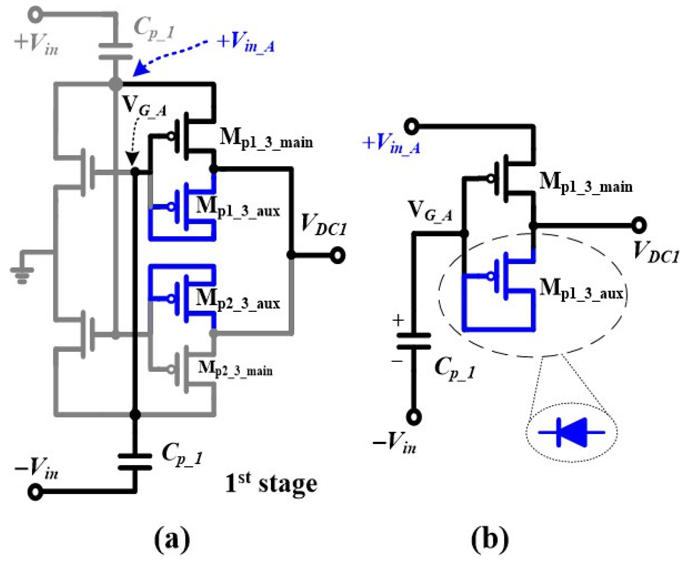
It is important to recall that both VDN and VDP in Equation (10) are closely linked to the ON-state resistance RDS_ON. Minimizing RDS_ON is desirable for improved performance; however, this comes with several design trade-offs that complicate the overall optimization process. To address this, a novel design strategy is introduced, as illustrated in Figure 6a. Two diode-connected PMOS devices are introduced to create auxiliary current paths. Because the circuit is symmetrical and driven by differential inputs, the discussion is limited to the upper switching branch, shown in Figure 6b.
In the positive half-cycle, +VIN exceeds −VIN, and PMOS Mp_N conducts once (+VIN_AVG_A) ≥ |VTHp_N|. A basic diagram is provided in Figure 6b. The gate potential VG_A is limited by the body diode linking the drain and bulk of the auxiliary PMOS Mp_N_aux and its source-gate voltage VSG. Evaluating the output-node voltages under these constraints yields the relationship that follows
VDC_OUT = VSG_aux + VCp_NVin
The voltage at the +VIN_A node can be written as
Vin_A = VSG_main + VCp_NVin
Here, the source-to-gate voltages of the auxiliary and main PMOS transistors are VSG_aux and VSG_main. Taking away Equation (14) from Equation (13) yields the DC output voltage, VDC_OUT, as
VDC_OUTVin_A = VSG_auxVSG_main
At this point, the terms VCP_N and Vin cancel out, and with additional simplification, the expression can be further reduced to its final form,
VDC_OUT = Vin_A − (VSG_mainVSG_aux)
When Vin falls below the output by roughly one threshold voltage VTH, the auxiliary PMOS transistor Mp_N_aux operates in weak inversion. As Vin rises and exceeds the output by at least VTH, this diode-connected device (VDS = VSG) shifts into strong inversion (saturation) [28]. The main PMOS Mp_N stays in the linear (ohmic) region, keeping RDS_ON low and conduction losses small. When the source node sits one VTH above the output, the diode current through Mp_N_aux can be approximated as follows [28]:
I S D 1 2 β V S G V T H _ p
solving VSG at the saturation region as
V S G V T H _ p + 2 I S D β
The approximate ohmic current flowing through Mp_N in the linear region is given by
I S D β V S G V T H _ p V S D
solving VSG at the ohmic region as
V S G V T H _ p + I S D β V S D
With
β = μ p C o x W L
Here, β is a technology-dependent constant that incorporates the hole mobility (µp), the gate oxide capacitance per unit area (Cox), and the geometric parameters of the transistor, namely the gate width (W) and length (L). By substituting Equations (18) and (20) into Equation (16), the resulting expression for VDC_OUT can be derived as
V D C _ O U T = V i n _ A V T H m a i n V T H a u x + I S D β V S D 2 I S D β
Equation (22) indicates that the diode-connected PMOS devices placed in the auxiliary paths serve as VTH compensators for the main PMOS transistors within the rectifier. PCE depends on the threshold voltage offset, the actual VTH of the conducting devices, the rectifier stage count, and the load current IL. By compensating the threshold drop, the auxiliary network lessens the impact of the equivalent series resistance introduced by the additional passive components, thus improving the total efficiency of the capacitor-enhanced CCDD rectifier. Consequently, the circuit achieves improved DC voltage extraction along with higher conversion efficiency.
To accurately evaluate the effect of this threshold-compensation scheme, all transistors in this work were intentionally designed with long channel lengths (L > Lmin) despite the use of a 65 nm CMOS process. Choosing device lengths substantially longer than the minimum—specifically 0.18 µm and 0.20 µm—suppresses short-channel effects such as velocity saturation and DIBL. This results in device behavior that more closely aligns with classical long-channel MOSFET characteristics, making the analytical square-law model in (17) a reasonable first-order approximation for the operating region of interest.
All simulations were performed using licensed Synopsys HSPICE together with the TSMC 65 nm CMOS PDK, which includes the foundry-supplied BSIM4 transistor models. The use of long-channel devices within a BSIM4-based simulation environment provides a consistent and practical framework for validating the analytical behavior predicted by the square-law model.
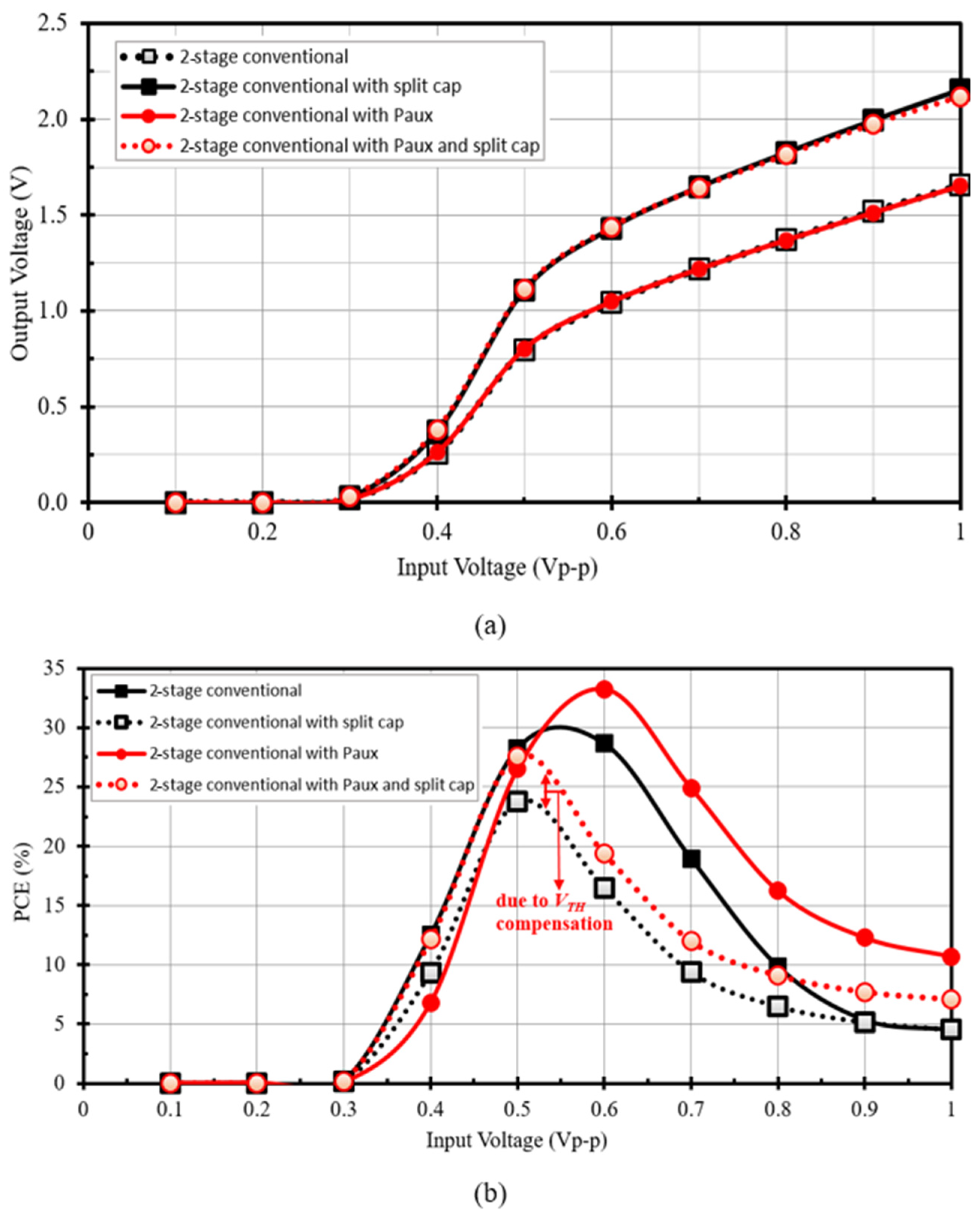
Figure 7 presents schematic-level simulation results (bond-pad and I/O-pad parasitics excluded) that compare several circuit variants. Each variant is evaluated at a 2.4-GHz RF sinusoidal input to highlight the influence of the split capacitors and auxiliary paths.

2.6. Indoor Light Energy Harvesting Rectifier Design

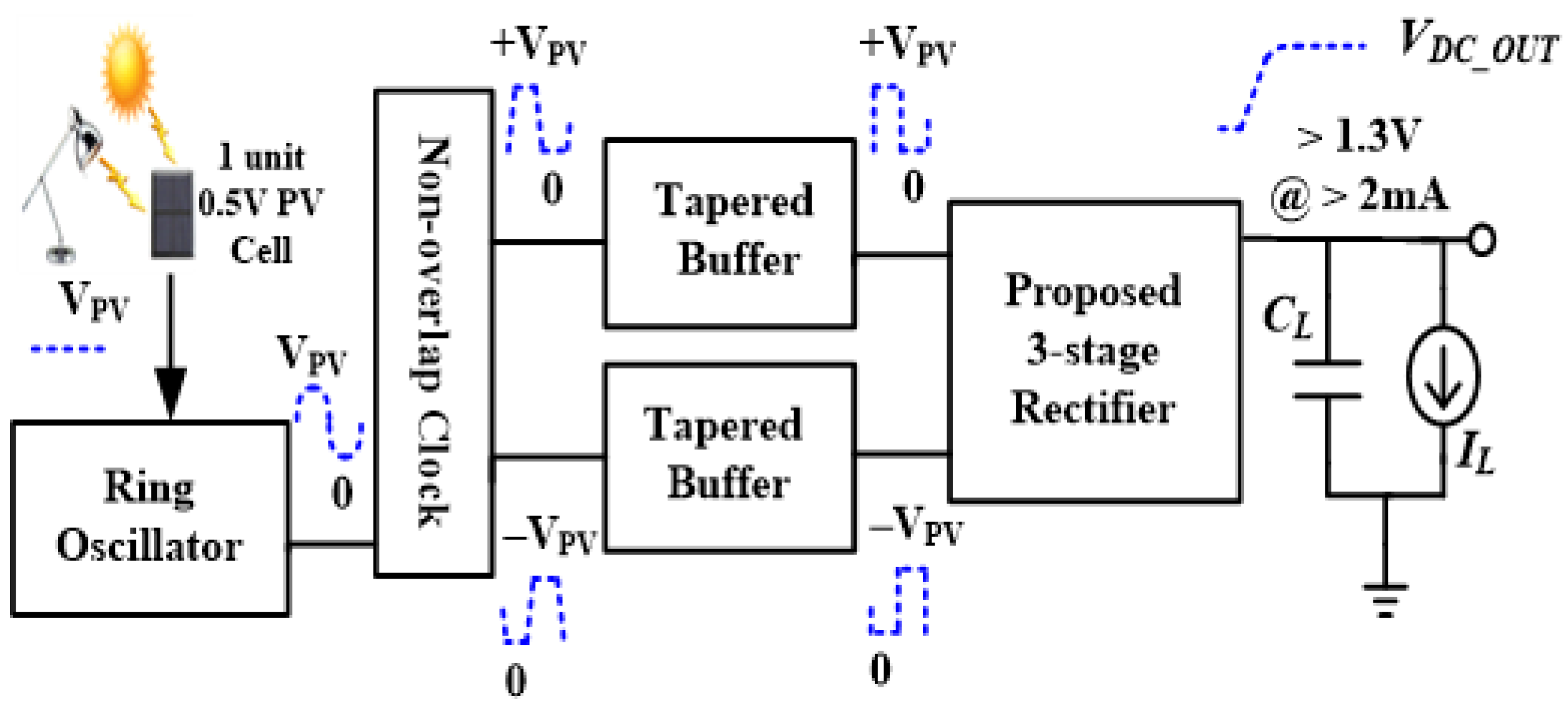
A three-stage rectifier based on the proposed technique was built for indoor light EH. Figure 8 presents the full block diagram of this system. As illustrated, a single unit PV cell with a nominal 0.5 V output voltage is used in this design. A ring oscillator is designed to convert the energy from the DC output voltage to AC. The operation frequency of the ring oscillator is selected to be 12.5 MHz so that the undesired switching loss can be minimized, and an optimum loading current can be maintained.
The AC signal generated by the oscillator is then fed to a non-overlapping clock generator. The output of the clock generator provides the required differential AC excitation to the rectifier through a tapered buffer. For consistency with the RF rectifier in the next subsection, the input AC amplitude used for both simulation and measurement of this 12.5 MHz rectifier is also referenced to a 50 Ω source impedance. All voltage and power values reported for this design follow this 50 Ω convention.
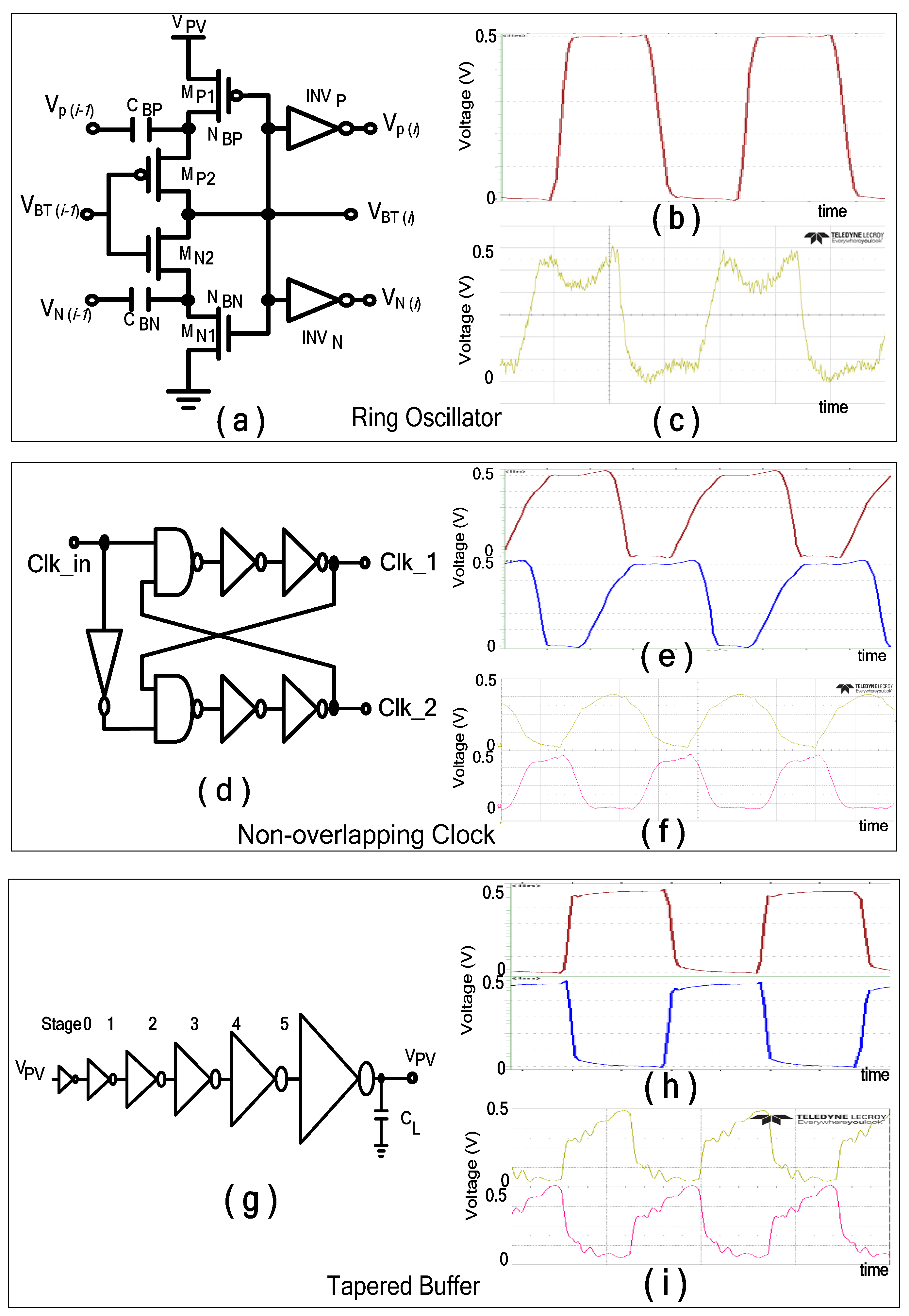
Figure 9 presents the schematic diagram along with the corresponding chip-level measurement results of the ring oscillator, non-overlapping clock generator, and output buffer.
The detailed circuit design and operational principles of these three building blocks were thoroughly discussed in our earlier work [29]. The ring oscillator and the non-overlapping clock only consumed a few nanowatts due to their digital switching capabilities. On the other hand, the taper buffer occupied the most significant area in the die to generate a robust pulsating signal and to drive the rectifier’s milliampere load requirements. The measured peak efficiency from the PV cell source to the rectifier was only around 35%.
The rectifier was set up according to the following baseline parameters:
  • The capacitor (CL) and load resistor (RL) were set to initial values of 1 nF and 100 Ω, respectively.
  • The pump capacitor CP was chosen to be 15× larger than each storage capacitor (CS1a and CS1b); thus, CP was set to 10 nF.
  • Initial transistor dimensions were PMOS width WP = 3 µm, NMOS width WN = 1 µm, and channel length L = 0.1 µm. Larger widths may later be selected to further lower RDS_ON
  • Device multiplicity was set with multiplier m = 500 and finger count f = 2.
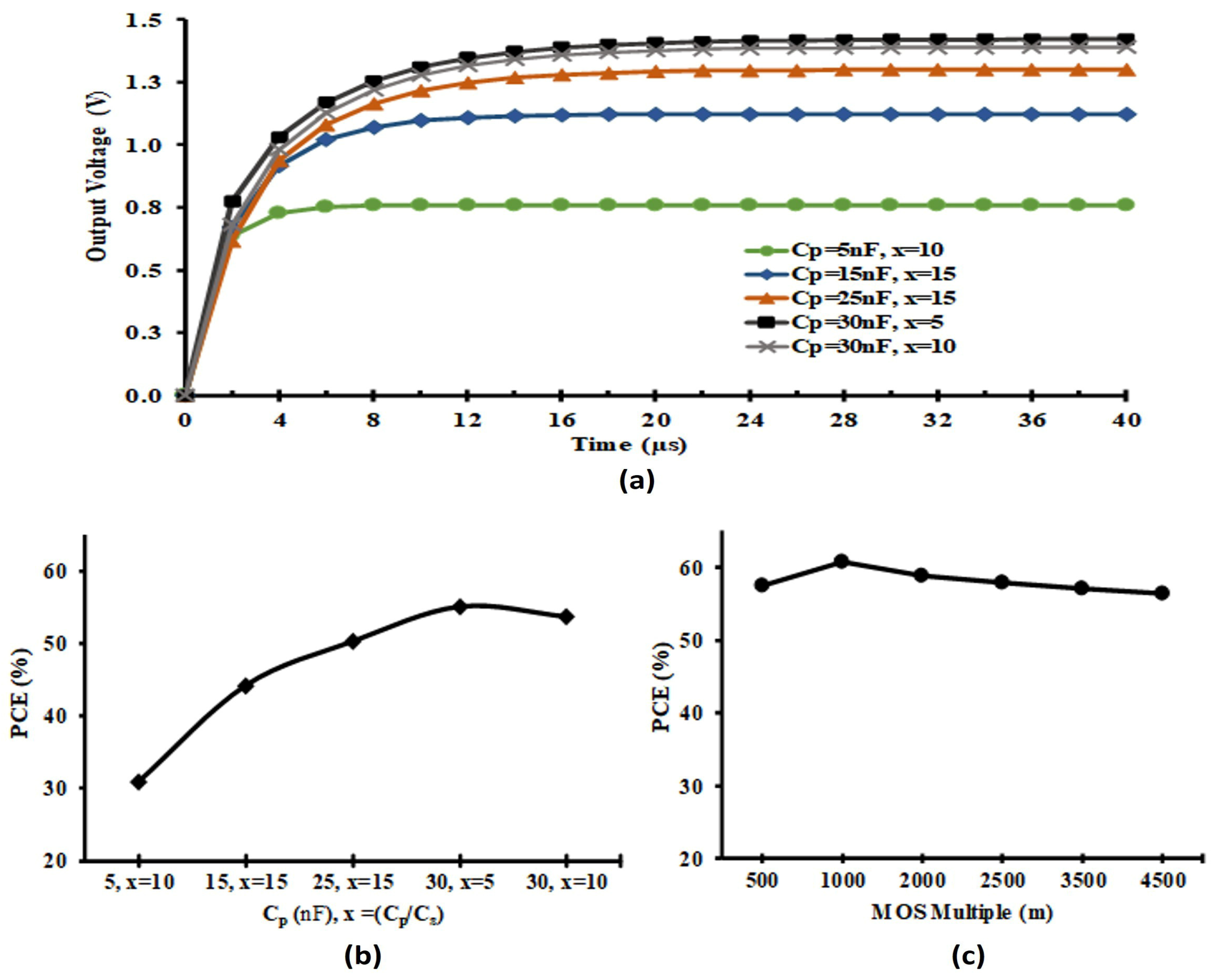
Earlier analysis showed that the DC output voltage of the rectifier depends heavily on the input AC amplitude and the values of capacitors Cs1a_b and Cp. To explore this dependency, a simulation study was conducted to examine how the ratio of these capacitors affects the DC output voltage. The results are shown in Figure 10. As shown in Figure 10a, the parametric simulation of the coupling capacitor Cp reveals that the output voltage begins to saturate when Cp = 30 nF and the capacitor ratio x = Cp/Cs1a_b = 5. Beyond this ratio, further increasing Cp does not lead to noticeable improvements in output voltage. A similar trend is observed in the parametric simulation of PCE, as illustrated in Figure 10b. Setting Cp = 30 nF and Cs1a = Cs1a_b = 6 nF provides the best trade-off, giving the highest simulated DC output voltage and a PCE of 55.1%. Because the DC level rises with the charge stored on Cp and Cs1a_b, efficiency improves up to this point. Beyond these capacitance values, however, additional loading from Cs1a_b exceeds the circuit’s capability, and PCE begins to fall. Additionally, Figure 10c shows that the rectifier achieves a peak simulated efficiency of 60.7% when the transistor multiplication factor is increased to m = 1000, as determined through a separate parametric simulation.
The transistor multiplication factor was determined through simulation to achieve optimal power conversion efficiency while providing sufficient current driving capability to support an output load ranging from 2 mA to 8 mA. As a result, an optimized DC output voltage of 1.98 V was achieved from an input voltage of 0.5 V.
Area–efficiency trade-offs are inherent in CMOS rectifier design. Increasing transistor multiplicity (m) and on-chip capacitor sizes reduces conduction loss and improves the voltage conversion ratio; however, these choices directly increase the silicon area and introduce larger parasitic capacitances, which can reduce the overall power conversion efficiency at higher frequencies. Conversely, reducing the number of rectifier stages or capacitor sizes decreases chip core area but limits the achievable output voltage. In this design, the selected transistor widths, capacitor sizes, and number of stages were chosen to meet the target output voltage and conversion ratio while keeping the chip area moderate and avoiding excessive parasitic-induced power losses.

2.7. Rectifier Design for 2.4 GHz RF Energy Harvesting

Designing the 2.4 GHz RF EH rectifier introduces additional challenges not encountered in the indoor-light version. Harmonic Balance analysis is performed with a CMOS RF model, a 50 Ω source, a 2.4 GHz carrier, and a swept input power range. At this frequency, the rectifier cannot drive large capacitors efficiently. As a result, the pumping capacitor Cp is limited to values between 0.2 pF and 1 pF, while the cross-coupled capacitors Cs1a_b are constrained to just a few femtofarads. This limitation significantly restricts the output current driving capability, with simulations indicating a maximum current of only 72.8 µA at the output node.
Using the same design approach as the indoor light EH rectifier, the starting values are set to Cp = 0.2 pF and CL = 1 pF, with an initial load resistance of 10 kΩ. Subsequent parametric simulations are performed to optimize key design variables—transistor multiplicity (m), number of fingers (f), and aspect ratio (W/L)—concerning output loading capability and input sensitivity.
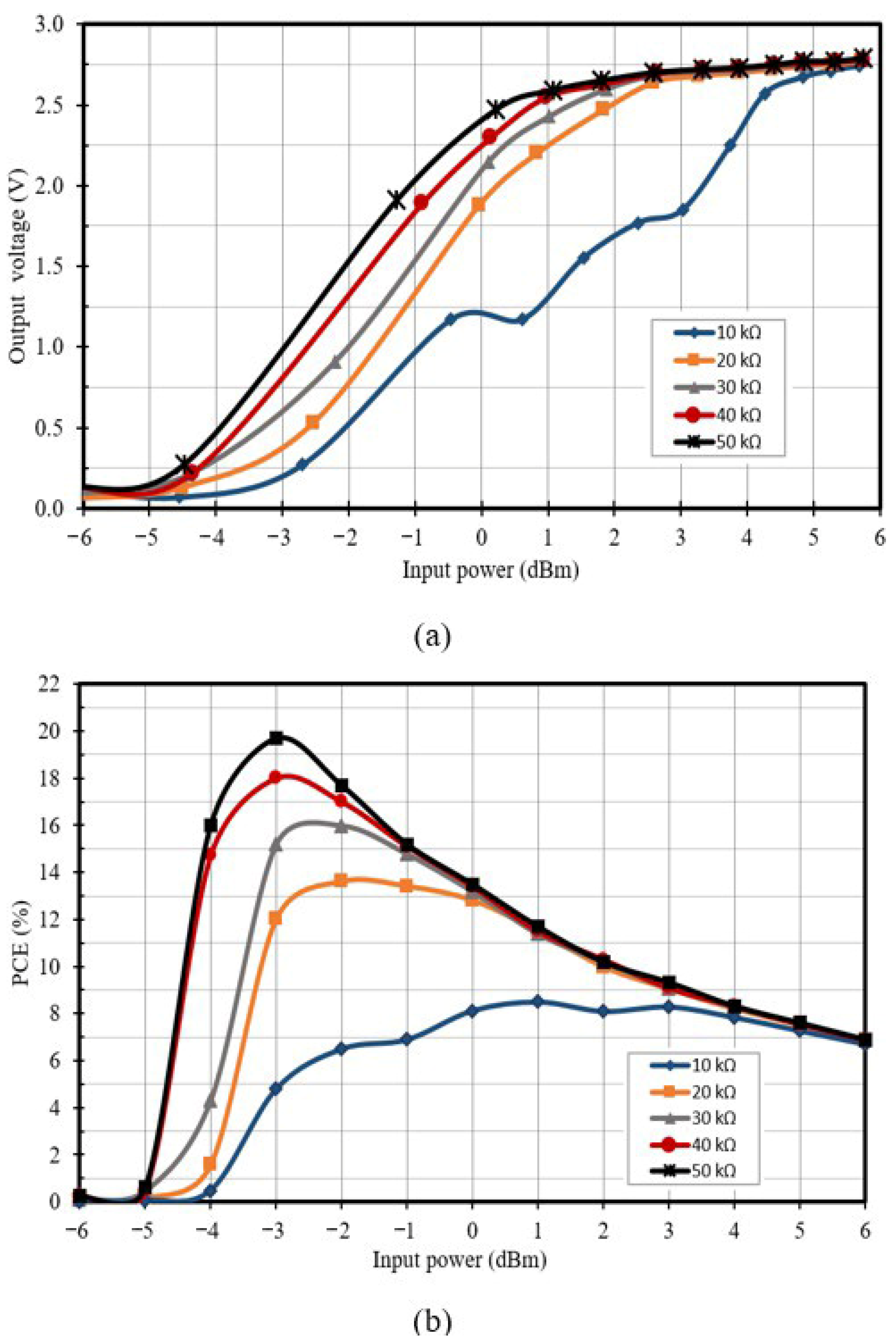
Figure 11a presents the simulated output voltage within the range of input power levels. With optimized capacitor and transistor parameters, the load resistance is further varied to assess the loading performance of the rectifier. The highest output voltage is observed when a load of 50 kΩ is applied, while lower resistance values lead to a degradation in output voltage. Figure 11b plots the rectifier’s PCE versus input power, indicating that peak efficiency is obtained with a 50 kΩ load.

3. Results

3.1. Measurement Setup

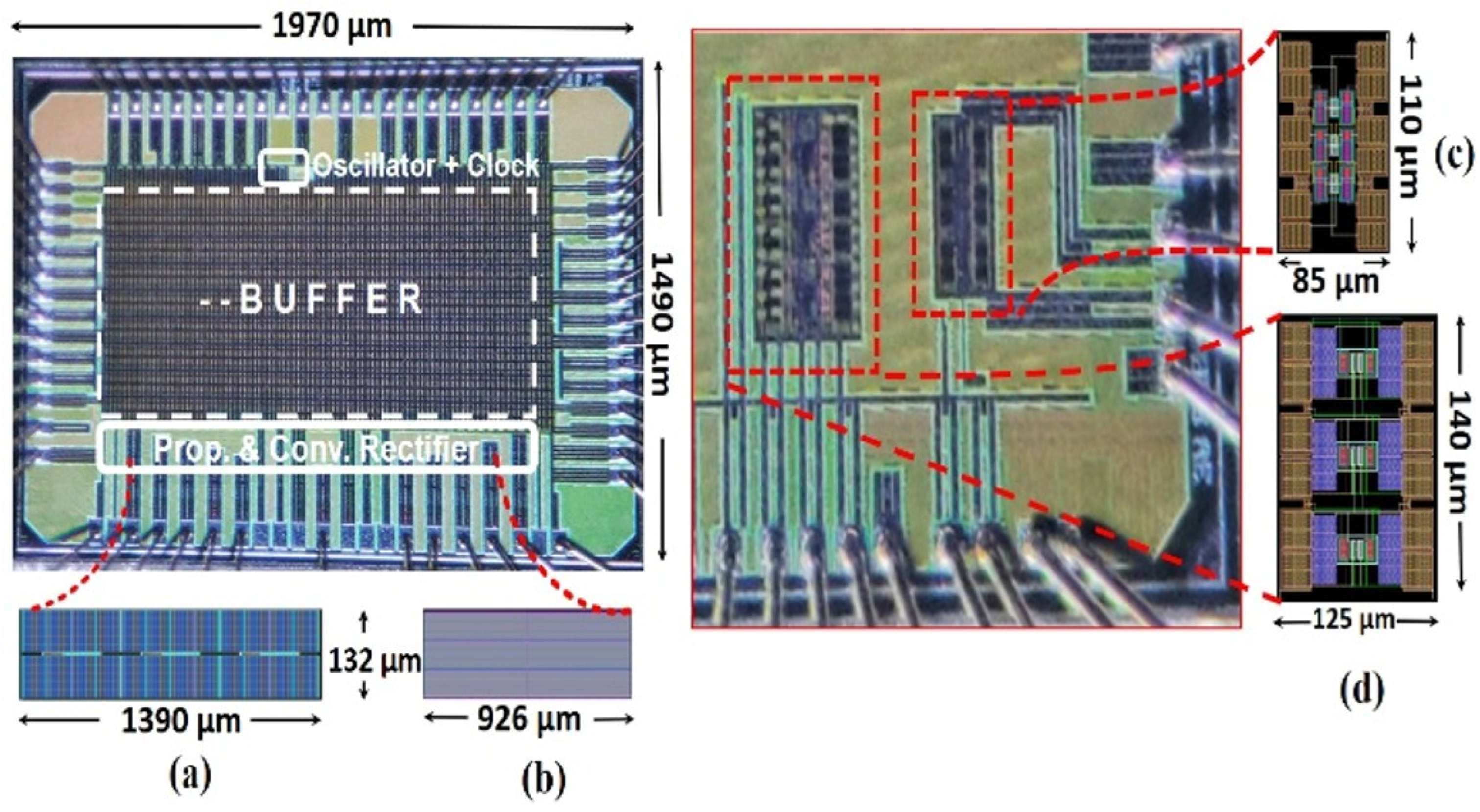
To validate the proposed architecture, four rectifier chips were fabricated using 65 nm 1P9M CMOS RF technology. Two units were aimed at indoor light energy harvesting, and two at 2.4 GHz RF harvesting. Figure 12 shows die photographs of all four chips. The indoor light rectifier occupies 0.183 mm2, while the 2.4 GHz version uses only 0.018 mm2. Each device is housed in a 44-pin quad flat package (QFP).
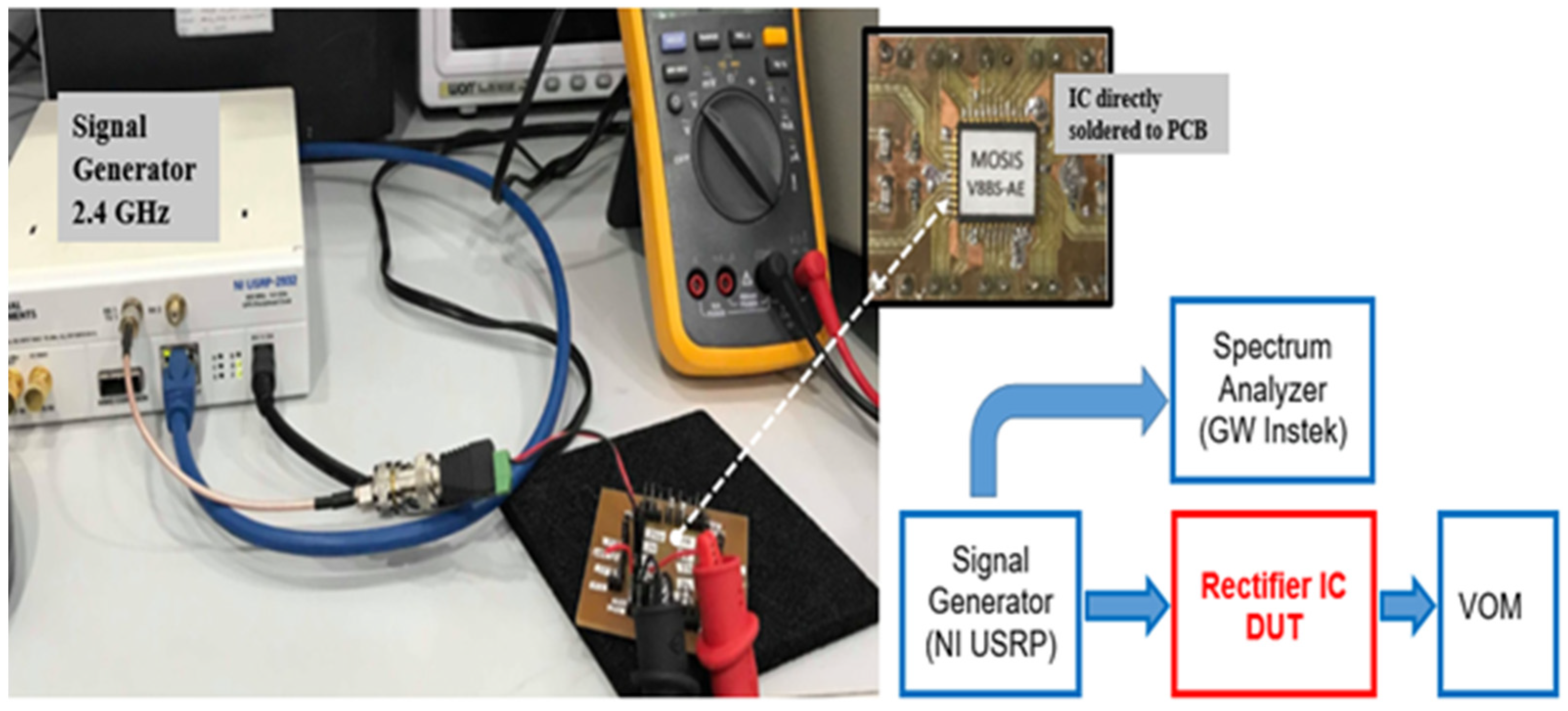
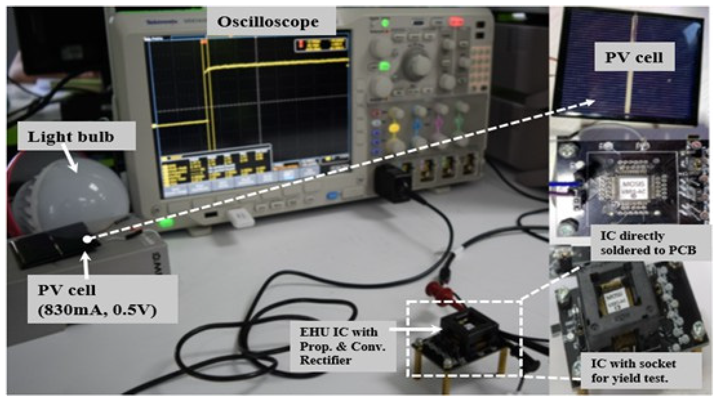
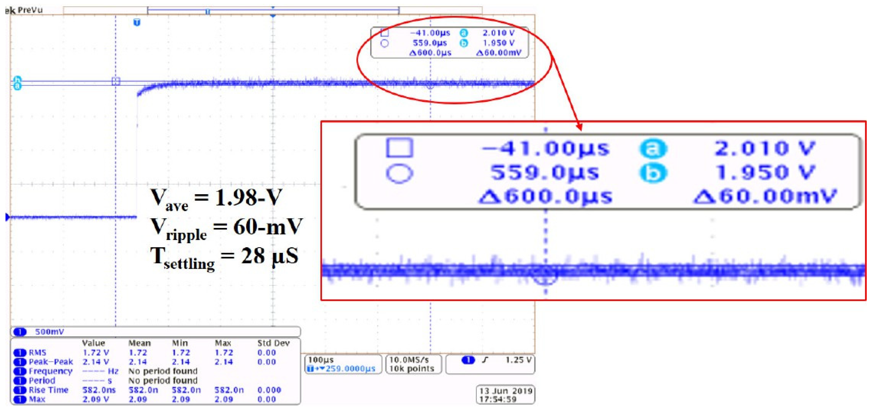
The 2.4 GHz rectifier was characterized using a signal generator (USRP Tx) and a spectrum analyzer (GW Instek) to evaluate its standalone RF-to-DC conversion performance, as shown in Figure 13. Due to the absence of a die-probing station, de-embedding of the measurements was not performed. Instead, pad and package parasitics were accounted for in both simulation and experimental evaluation, ensuring that the results reflect the fabricated device. In this study, the rectifier was intentionally tested without an LC matching network, so that the measured efficiency corresponds solely to the rectifier’s intrinsic performance. This setup provides a first-order assessment of the rectifier’s behavior at the target frequency. Whereas, to characterize the performance of the designed rectifier for the indoor light PV energy harvesting system, a mixed-domain oscilloscope (Tektronix MDO4104C) and two digital multimeters were used, following the measurement setup shown in Figure 14. Figure 15 presents the time-domain waveform of the indoor light PV-EH rectifier, including a zoomed-in view of the ripple voltage. The measured ripple is approximately 60 mV, with an average output voltage of 1.98 V and a settling time of 28 µs under a 600 Ω load and CL = 5 nF.
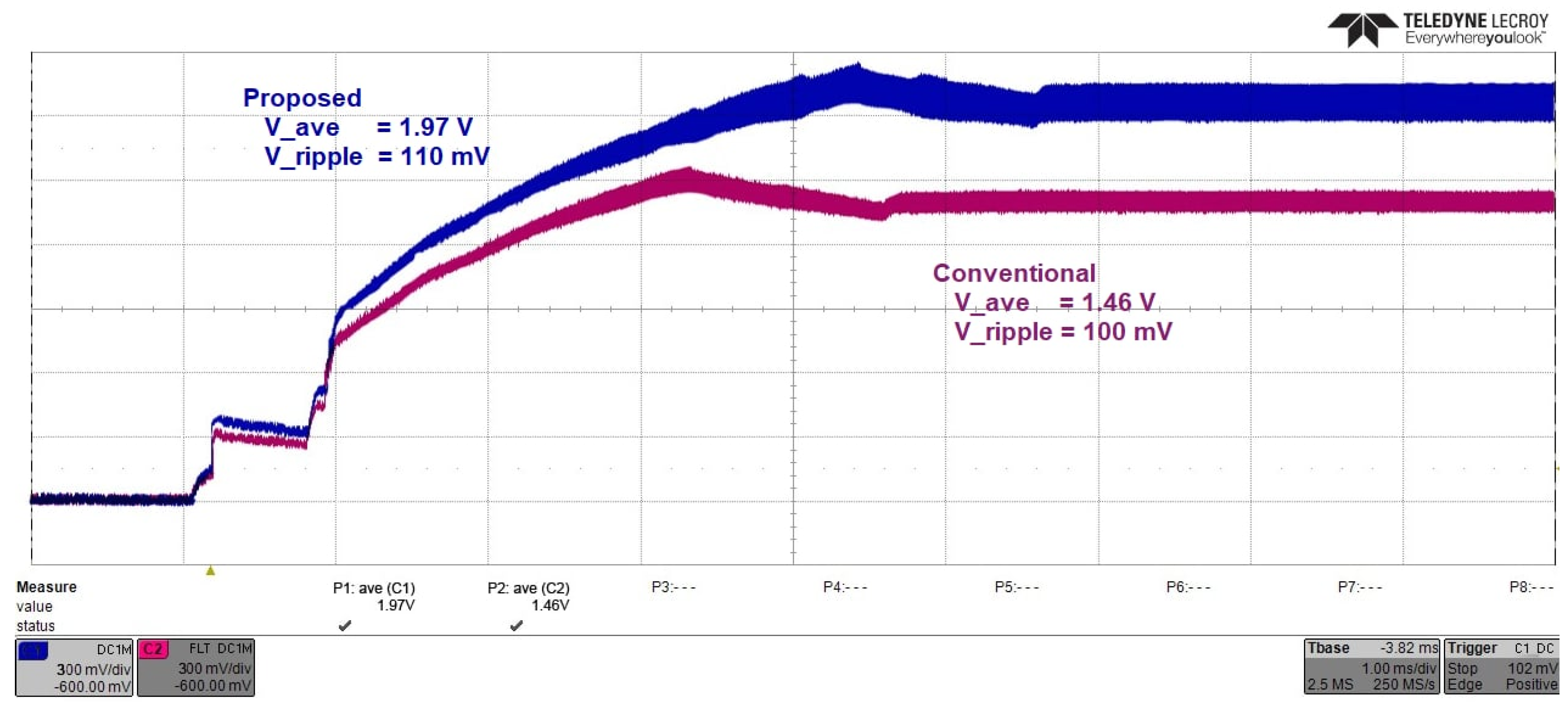
Figure 16 shows a snapshot captured from the Teledyne LeCroy oscilloscope by the industry partner, comparing the chip performance of the proposed and conventional rectifiers. The test conditions were set to Vin = 0.5 V, RL = 600 Ω, CL = 1 nF, and f = 12.5 MHz for the indoor light energy harvesting block. The proposed rectifier achieved an average output voltage of 1.97 V with minimal ripple. Since signal parasitics—including I/O pads, bond pads, bonding wires, and package leads—were modeled in the post-layout simulation, the measured results closely match the simulation. In contrast, the conventional rectifier produced an average voltage of 1.46 V with a 100 mV ripple.

3.2. Measured Versus Simulated Output Waveforms

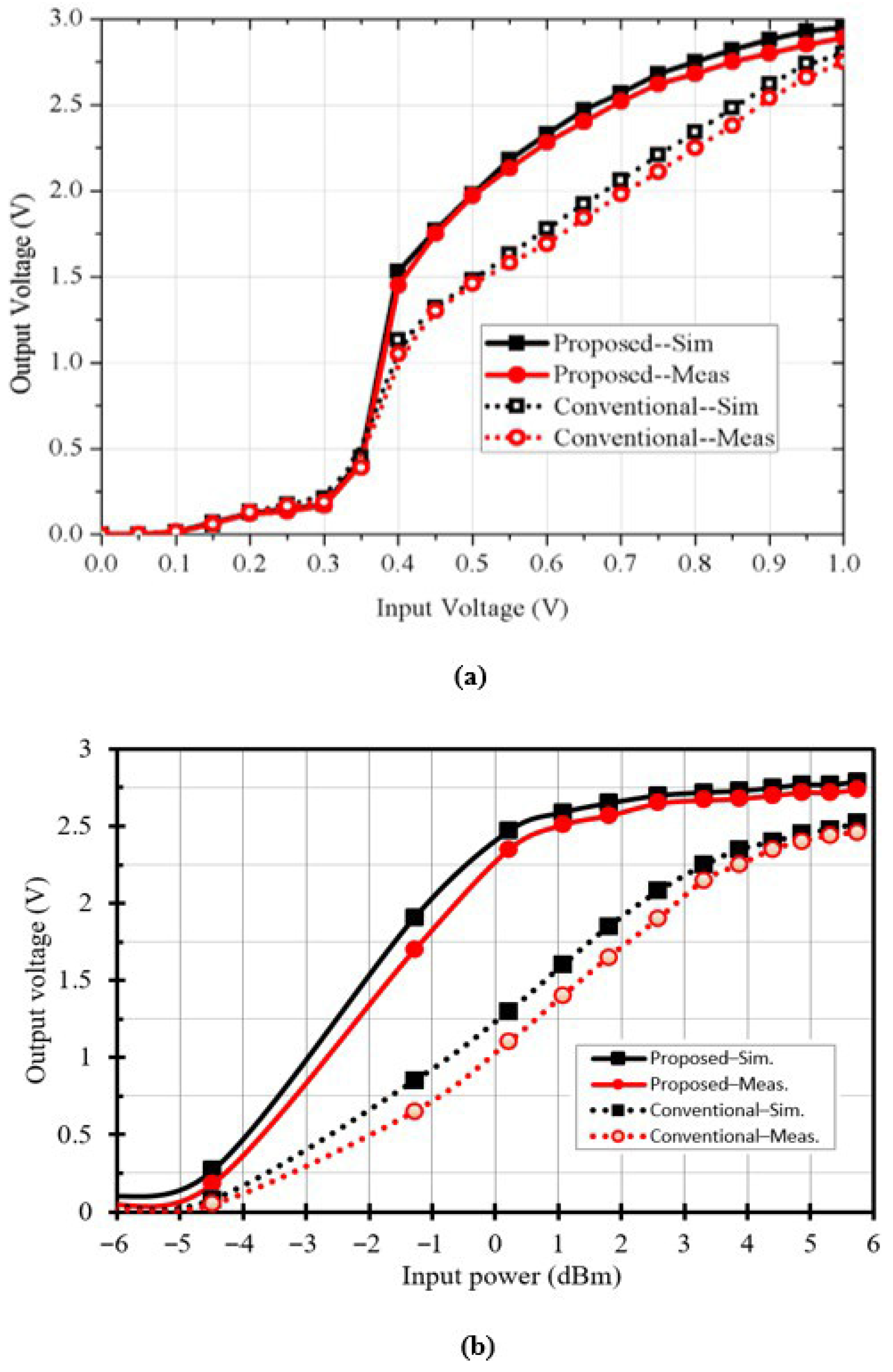
A comparison of simulated and measured output voltages for the first design is presented in Figure 17a. With the input voltage swept from 0.1 V to 1 V, results indicate that the first design delivers enhanced performance starting from an input threshold of approximately 0.45 V. Figure 17b plots the second design’s measured output voltage versus input power, and the data closely match the simulated curve. Across the −2 dBm to 2 dBm input-power range, the second design delivers a higher output voltage than the conventional reference design.
Minor deviations between the measured and simulated values arise from probe and cable insertion losses, RF pad parasitics, and the finite accuracy of the signal generator, vector network analyzer, and digital multimeter used in the bench setup. These measurement-related factors explain the small offsets observed in the indoor light rectifier’s results.

3.3. Voltage Conversion Ratio and Power Conversion Efficiency

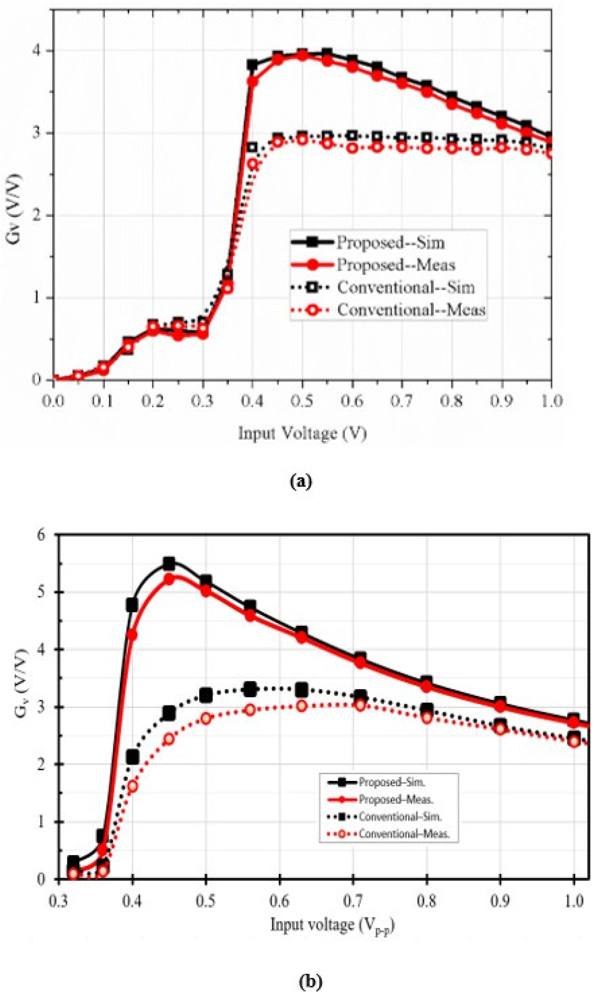
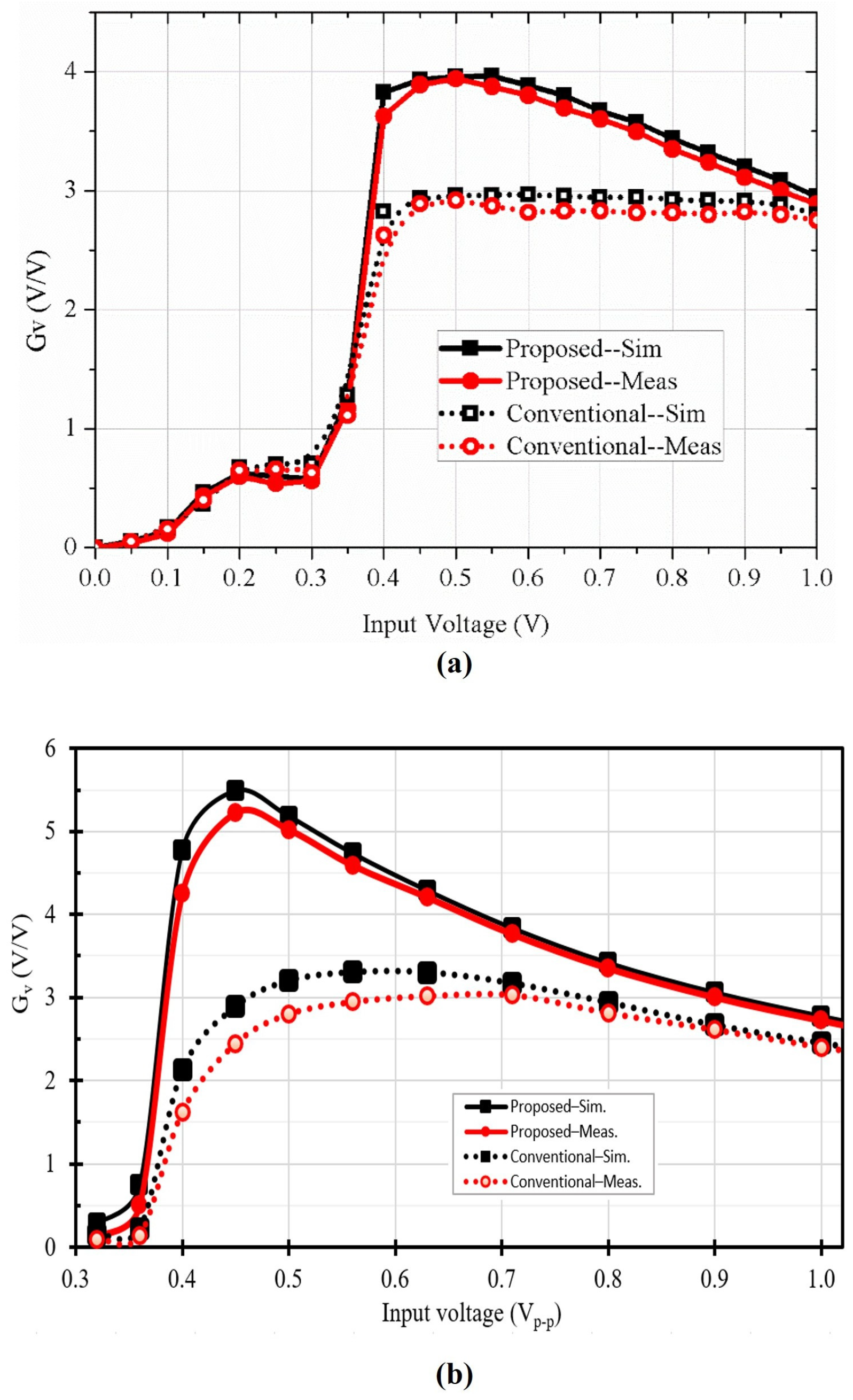
The calculated VCRs for both designs are presented in Figure 18a and Figure 18b, respectively, alongside those of conventional designs for benchmarking. The first design achieves a VCR of 3.94, compared to 2.92 for the conventional implementation. The second design attains a VCR of 5.02, exceeding the 2.8 measured for the conventional 2.4 GHz RF EH rectifier. For consistency, the input power values were converted from dBm to peak-to-peak voltage.
The measured PCE of the designed rectifiers is presented in Figure 19. It is important to note that different EH applications face distinct design constraints, leading to varying performance targets. Figure 19a plots PCE versus a load resistance sweep spanning 100 Ω to 1 kΩ to determine the optimum operating point for indoor light use. The conventional configuration exhibits a marginally greater maximum PCE compared with the proposed unit. In testing, the new rectifier reaches approximately 58.7% PCE at a 600 Ω load, about 2.1% lower than the reference design. This modest deficit is attributed to the equivalent series resistance inherent in the cross-coupled capacitors. Even so, the same graph highlights a clear gain in output voltage for the proposed design, confirming its effectiveness.
Figure 19b shows the 2.4 GHz RF rectifier characterized with a fixed 50 kΩ load while the input power is swept. The peak PCE is 17.5%, around 2.2% below that of the reference circuit; nevertheless, the proposed rectifier delivers a higher output voltage over the entire input-power range.
Across Figure 17, Figure 18 and Figure 19, the minor discrepancies between the measured and simulated curves can be attributed to typical sources of measurement uncertainty, including probe and cable insertion losses, variation in the RF pad and interconnect parasitics captured during post-layout extraction, and the finite accuracy of the signal generator, vector network analyzer, and digital multimeter used in the laboratory setup. These effects are commonly encountered in CMOS-based rectifier measurements and explain the small offsets observed while confirming the overall consistency between the simulated predictions and the measured chip performance.

3.4. Comparison with Previous Works

Table 2 provides a detailed comparison between the proposed three-stage, capacitor-assisted CCDD rectifier and earlier reported designs. As the table shows, the presented designs achieve improved VCRs for both indoor light and 2.4-GHz RF EH scenarios, despite a slightly lower PCE relative to some state-of-the-art implementations. Notably, the VCR achieved by the second design at 2.4 GHz outperforms those reported in [2,3,4,5,6,7,8,9,10,11,12,13,14,15,16,17,18,19,20,21,22,23,24,25,26,27,28,29,30]. Although the design in [31] reports a higher VCR, it relies on an eight-stage configuration and suffers from a relatively low PCE of just 14%. In contrast, the proposed four-stage rectifier achieves a VCR exceeding that of [32] while maintaining the same peak efficiency of 17.5%, with a consistent 0.5 V input voltage.
Overall, the proposed capacitor-based CCDD architecture with auxiliary paths enables high output voltage generation while maintaining competitive efficiency, making it well-suited for energy harvesting applications that require both voltage boosting and compact design.
The improved voltage conversion and power efficiency achieved by the proposed rectifier make it a strong candidate for integration in complete energy harvesting systems. To further contextualize its role in practical applications, the following subsection discusses its potential integration with dynamic regulation and energy storage circuits recently explored in the literature.

3.5. Dynamic Regulation and Energy Storage Integration

Dynamic regulation is crucial for maintaining stable energy delivery and improving the long-term reliability of energy harvesting (EH) systems. In practical designs, the rectifier output is connected to a storage component such as a microbattery, supercapacitor, or thin-film capacitor together with a power-management circuit that regulates charging and discharging under variable input conditions. These regulation stages help balance harvested energy, mitigate transient voltage drops, and support the continuous operation of wireless sensor nodes.
Recent work emphasizes dynamically controlled storage and regulation mechanisms for sustainable EH systems. For example, Ref. [33] proposed a dynamically synergistic regulation method for rotation-based energy harvesters and achieved improved output stability through real-time impedance adaptation. In a related contribution, Ref. [34] reviewed intelligent mechanical energy harvesting frameworks that integrate adaptive control to optimize energy flow and enhance storage utilization. At the network level, Ref. [35] showed that distributed real-time regulation strategies for shared energy storage systems can improve voltage balance and frequency regulation in renewable-powered settings.
Table 2. Performance summary and comparison with previous works.
ReferenceCircuitOperatingInputOutputNo. ofVCRPeakLoad CurrentCMOS
TechniquesFrequencyAmplitudeVoltageStages(V/V)PCE (%)RL, ILOADTech. (µm)
(V)(V)
DESIGN 1 [InLight EH]
This workAuxiliary MOS12.5 MHz0.51.9733.9458.72–8 mA0.065
and Capacitor
[23] Conventional, 2009 °Conventional12.5 MHz0.51.4632.9260.82–8 mA0.065
[17] Chong, 2019 *aCCDM *a
Shared-capacitor
12.5 MHz0.51.6533.30b2–8 mA0.065
coupling (ICC) *a
[25] Grasso, 2019 *aBody-voltage12.5 MHz0.51.5533.10b2–8 mA0.065
control scheme *a
[36] Haddad, 2016Greinacher ULP13.56 MHz0.51.9033.80720.01 mA0.25
[30] Guler, 2019Diode
Reconfigurable
13.56 MHz2.4 †4.92 †32.05762 kΩ0.35
VM
DESIGN 2 [RF EH]
This workAuxiliary MOS2.4 GHz0.5 ‡2.5135.0217.550 kΩ0.065
and Capacitor
[23] Conventional, 2009 °Conventional2.4 GHz0.5 ‡1.3932.8019.750 kΩ0.065
[17] Chong, 2019 *aCCDM *a
Shared-capacitor
2.4 GHz0.5 ‡2.2034.44b50 kΩ0.065
coupling (ICC) *a
[25] Grasso, 2019 *aBody-voltage2.4 GHz0.5 ‡2.0534.10b50 kΩ0.065
[16] Moghaddam, 2017control scheme *a
CCDM with Lower
2 GHz0.5 ‡2.48 †34.9625 †50 kΩ0.13
DC Feeding (LDCF)
2 GHz2.0 ‡3.5 † 1.7565 †10 kΩ
[31] Lau, 2017CCDM with DC-boosted2.45 GHz0.5 ‡1.35 †22.748 †5 kΩ0.065
gate bias
2.45 GHz0.159 ‡1.04 † 6.5459.629 kΩ
[20] Lo, 2017CCDM with HP Path900 MHz0.1 ‡1.0 †510.036.5147 kΩ0.065
(LVTGP, LVTL_P)
900 MHz0.45 ‡2.5 † 5.55
[32] Abouzied, 2017Reconfigurable Greinacher915 MHz0.5 ‡2.35 †24.7261 MΩ/PMU0.18
doubler with LC matching
915 MHz0.5 ‡2.35 †44.717.5 †
915 MHz0.079 ‡1.0 †812.6614 †
° Measurement results were redesigned/reproduced in this work to operate at 12.5 MHz, 2.4 GHz. *a Simulation results are redesigned/reproduced in this work to operate at 12.5 MHz, 2.4 GHz; −2 dBm input ≈ 0.5 Vp-p. b Simulation result not taken; † data extrapolated/estimated from graph; ‡ data Pin (dBm) sensitivity converted to Vp-p.
Integrating the proposed capacitor-boosted CCDD rectifier with similar dynamic regulation circuits can further stabilize its DC output, especially under fluctuating illumination or RF conditions. This integration enables efficient hybrid energy harvesting and storage, making the architecture suitable for autonomous and self-sustaining Internet-of-Things (IoT) and wireless sensor network (WSN) nodes that require reliable energy availability even when sources are intermittent.

4. Conclusions

This paper presents novel circuit design techniques for CMOS-based rectifiers that significantly enhance both VCR and PCE. Utilizing these methods, two rectifiers were designed and fabricated using 65 nm CMOS technology. The first design operates at 12.5 MHz, while the second targets 2.4 GHz applications. To validate the proposed techniques, a theoretical analysis was conducted, and a three-stage, capacitor-based, cross-coupled, differential-driven (CCDD) architecture was employed for both designs. Compared to existing state-of-the-art solutions, the proposed rectifiers demonstrate notable improvement. Under a load of 600 Ω, the first rectifier achieves a peak VCR close to 4 and a measured PCE of approximately 58.7%. Moreover, it can deliver more than 2 mA of current, which is sufficient for quickly charging external energy storage components such as batteries or supercapacitors. In the second design, targeting RF energy harvesting, the VCR exceeds 5 with a PCE of 17.5% under a load of 50 kΩ. Although the output current is limited to 70 µA, it remains suitable for typical RF EH scenarios. Overall, the experimental results confirm that the proposed design strategies are highly effective for developing efficient CMOS-based rectifiers. The resulting rectifiers offer a cost-effective power source for battery-less wireless sensors and other emerging energy-autonomous devices.

Author Contributions

Conceptualization, J.H. and X.Z.; methodology, J.H. and R.S.; simulation, J.H., R.S. and X.Z.; chip testing, J.H., R.S., G.F.P. and J.T.; validation, G.F.P., J.T. and Y.S.; formal analysis, J.H.; resources, X.Z. and Y.S.; writing—original draft preparation, J.H.; writing—review and editing, X.Z., J.T. and Y.S.; supervision, X.Z.; project administration, J.H. and X.Z.; funding acquisition, X.Z. and Y.S. All authors have read and agreed to the published version of the manuscript.

Funding

This research was funded by the Philippine DOST-PCIEERD and the Australian Research Council DE160101032.

Data Availability Statement

The original contributions presented in this study are included in the article. Further inquiries can be directed to the corresponding author.

Acknowledgments

This paper would like to acknowledge the support provided by the Department of Science and Technology—Science Education Institute (DOST-SEI) through the Engineering for Research and Development (ERDT) Program, together with the Center of Integrated Circuits Design (CICD-Microlab) of the Mindanao State University-Iligan Institute of Technology (MSU-IIT). Progress in this work is utilized as a preliminary circuit design block of the funded project by the Department of Science and Technology (DOST), Philippines, and monitored by DOST-PCIEERD for the project titled Energy Harvesting for Battery-less IoT Device Operation under the program Center for Integrated Circuits and Devices Research (CIDR).

Conflicts of Interest

The authors declare no conflicts of interest.

References

  1. Hora, J.A.; Zhu, X.; Dutkiewicz, E. Design of High Voltage Output for CMOS Voltage Rectifier for Energy Harvesting Design. In Proceedings of the IEEE Wireless Power Transfer Conference (WPTC), London, UK, 18–21 June 2019; pp. 40–44. [Google Scholar] [CrossRef]
  2. Hakiri, P.; Berthou, P.; Gokhale, A.; Abdellatif, S. Pubziesh/Subscribe-Enabled Software Defined Networking for Efficient and Scalable IoT Communications. IEEE Commun. Mag. 2015, 53, 48–54. [Google Scholar] [CrossRef]
  3. Chandravee, B.; Caubel, J.J.; Kim, K.; Cheng, E.; Dhinakaran, A.; Agogino, A.M.; Martin, R.A. Sensor-Based Predictive Modeling for Smart Lighting in Grid-Integrated Buildings. IEEE Sens. J. 2014, 14, 4216–4229. [Google Scholar] [CrossRef]
  4. Shin, M.; Joe, I. Energy Management Algorithm for Solar-Powered Energy Harvesting Wireless Sensor Node for Internet of Things. IET Commun. 2016, 10, 1508–1521. [Google Scholar] [CrossRef]
  5. Prijić, A.; Vračar, L.; Pavlović, Z.; Kostić, L.; Prijić, Z. The Effect of Flat Panel Reflectors on Photovoltaic Energy Harvesting in Wire-less Sensor Nodes under Low Illumination Levels. IEEE Sens. J. 2015, 15, 7105–7111. [Google Scholar] [CrossRef]
  6. Stoopman, M.; Philips, K.; Serdijn, W.A. An RF-Powered DLL-Based 2.4-GHz Transmitter for Autonomous Wireless Sensor Nodes. IEEE Trans. Microw. IEEE Trans. Microw. Theory Tech. 2017, 65, 2399–2408. [Google Scholar] [CrossRef]
  7. Kuhn, V.; Lahuec, C.; Seguin, F.; Person, C. A Multi-Band Stacked RF Energy Harvester with RF-to-DC Efficiency up to 84%. IEEE Trans. Microw. Theory Technol. 2015, 63, 1768–1778. [Google Scholar] [CrossRef]
  8. Zhang, H.; Guo, Y.; Zhong, Z.; Wu, W. Cooperative Integration of RF Energy Harvesting and Dedicated WPT for Wireless Sensor Networks. IEEE Microw. Wirel. Compon. Lett. 2019, 29, 291–293. [Google Scholar] [CrossRef]
  9. Hou, L.; Tan, S.; Zhang, Z.; Bergmann, N.W. Thermal Energy Harvesting WSNs Node for Temperature Monitoring in IIoT. IEEE Access 2018, 6, 35243–35249. [Google Scholar] [CrossRef]
  10. Charmaniam, S.; Baghaee, S.; Ulusam, H.; Zorlu, O.; Biyikoglu, E.-U.; Kulah, H. Implementation of Energy-Neutral Operation on Vibration Energy Harvesting WSN. IEEE Sens. J. 2019, 19, 3092–3099. [Google Scholar] [CrossRef]
  11. Fan, S.; Wei, R.; Zhao, L.; Yang, X.; Leng, L.; Feng, P.-X.-L. An Ultralow Quiescent Current Power Management System with Maximum Power Point Tracking (MPPT) for Batteryless Wireless Sensor Applications. IEEE Trans. Power Electron. 2018, 33, 7326–7337. [Google Scholar] [CrossRef]
  12. Jeon, K.E.; She, J.; Xue, J.; Kim, S.-H.; Park, C. LuxBeacon: A Batteryless Beacon for Green IoT: Design, Modeling, and Field Test. IEEE Internet Things J. 2019, 6, 5901–5912. [Google Scholar] [CrossRef]
  13. Sun, Z.; Chew, K.W.R.; Tang, H.; Yu, G.; Siek, L. A 0.42-V Input Boost DC-DC Converter with Pseudo-Digital Pulsewidth Modulation. IEEE Trans. Circuits Syst. II Express Briefs 2014, 61, 634–638. [Google Scholar] [CrossRef]
  14. Jhang, J.-J.; Wu, H.-H.; Tsu, T.; Wei, C.-L. Design of a Boost DC-DC Converter with 82-mV Startup Voltage and Fully Built-in Startup Circuits for Harvesting Thermoelectric Energy. IEEE Solid-State Circuits Lett. 2020, 3, 54–57. [Google Scholar] [CrossRef]
  15. Mandal, S.; Sarpeshkar, R. Low-Power CMOS Rectifier Design for RFID Applications. IEEE Trans. Circuits Syst. I Regul. Pap. 2007, 54, 1177–1188. [Google Scholar] [CrossRef]
  16. Moghaddam, A.K.; Chuah, J.H.; Ramiah, H.; Ahmadian, J.; Mak, P.I.; Martins, R.P. A 73.9%-Efficiency CMOS Rectifier Using a Lower DC Feeding (LDCF) Self-Body-Biasing Technique for Far-Field RF Energy-Harvesting Systems. IEEE Trans. Circuits Syst. I Regul. Pap. 2017, 64, 992–1002. [Google Scholar] [CrossRef]
  17. Chong, G.; Ramiah, K.; Yin, J.; Rajendran, J.; Wong, W.R.; Mak, P.-I.; Martins, R.P. CMOS Cross-Coupled Differential-Drive Rectifier in Subthreshold Operation for Ambient RF Energy Harvesting: Model and Analysis. IEEE Trans. Circuits Syst. II Express Briefs 2019, 66, 1942–1946. [Google Scholar] [CrossRef]
  18. Chong, G.; Ramiah, H.; Yin, J.; Rajendran, J.; Wong, W.R.; Mak, P.-I.; Martins, R.P. A Wide-PCE-Dynamic-Range CMOS Cross-Coupled Differential-Drive Rectifier for Ambient RF Energy Harvesting. IEEE Trans. Circuits Syst. II Express Briefs 2019, 68, 1743–1747. [Google Scholar] [CrossRef]
  19. Valenta, C.R.; Durgin, G.D. Harvesting Wireless Power: Survey of Energy-Harvester Conversion Efficiency in Far-Field, Wireless Power Transfer Systems. IEEE Microw. Mag. 2014, 15, 108–120. [Google Scholar] [CrossRef]
  20. Li, B.; Shao, X.; Shahshahan, N.; Goldsman, N.; Salter, T.; Metze, G.M. An Antenna Co-Design Dual Band RF Energy Harvester. IEEE Trans. Circuits Syst. II Express Briefs 2013, 60, 352–366. [Google Scholar] [CrossRef]
  21. Nakamoto, H.; Yamazaki, D.; Yamamoto, T.; Kurata, H.; Yamada, S.; Mukaida, K.; Ninomiya, T.; Ohkawa, T.; Masui, S.; Gotoh, K. A Passive UHF RF Identification CMOS Tag IC Using Ferroelectric RAM in 0.35 µm Technology. IEEE J. Solid-State Circuits 2007, 42, 101–110. [Google Scholar] [CrossRef]
  22. Liu, D.-S.; Li, F.-B.; Zou, X.-C.; Liu, Y.; Hui, X.-M.; Tao, X.-F. New Analysis and Design of a RF Rectifier for RFID and Implantable. Sensors 2011, 11, 6494–6508. [Google Scholar] [CrossRef]
  23. Kotani, K.; Sasaki, A.; Ito, T. High-Efficiency Differential-Drive CMOS Rectifier for UHF RFIDs. IEEE J. Solid-State Circuits 2009, 44, 3011–3018. [Google Scholar] [CrossRef]
  24. Kotani, K.; Ito, T. High-Efficiency CMOS Rectifier Circuit with Self-VTH-Cancellation and Power Regulation Functions for UHF RFIDs. In Proceedings of the IEEE Asian Solid-State Circuits Conference, Jeju, Republic of Korea, 12–14 November 2007; p. 119. [Google Scholar] [CrossRef]
  25. Grasso, L.; Sorbello, G.; Ragonese, E.; Palmisano, G. Codesign of Differential-Drive CMOS Rectifier and Inductively Coupled Antenna for RF Harvesting. IEEE Trans. Microw. Theory Technol. 2019, 68, 365–376. [Google Scholar] [CrossRef]
  26. Lu, Y.; Dai, H.; Huang, M.-K.; Law, S.-W.; Sin, S.-P.U.; Martins, R.P. A Wide Input Range Dual-Path CMOS Rectifier for RF Energy Harvesting. IEEE Trans. Circuits Syst. II Express Briefs 2017, 64, 166–170. [Google Scholar] [CrossRef]
  27. Gao, H.; Matters-Kammerer, M.; Milosevic, D.; Linnarts, J.-P.M.G.; Baltus, P. A Design of 2.4 GHz Rectifier in 65nm CMOS with 31% Efficiency. In Proceedings of the IEEE 20th Symposium on Communications and Vehicular Technology in the Benelux (SCVT), Namur, Belgium, 21 November 2013; 2013. [Google Scholar] [CrossRef]
  28. Yi, J.; Ki, W.-H.; Tsui, C.-Y. Analysis and Design Strategy of UHF Micro-Power CMOS Rectifiers for Micro-Sensor and RFID Applications. IEEE Trans. Circuits Syst. I Regul. Pap. 2007, 54, 105–113. [Google Scholar] [CrossRef]
  29. Hora, J.A.; Mayormita, M.A.; Rebolos, J.R.C.; Zhu, X.; Dutkiewicz, E. On-Chip Inductor-Less Indoor Light Energy Harvesting WSN/IoT Device Design. In Proceedings of the 2019 13th International Conference on Sensing Technology (ICST), Sydney, NSW, Australia, 2–4 December 2019; pp. 1–6. [Google Scholar] [CrossRef]
  30. Guler, U.; Jia, Y.; Ghovanloo, M. A Reconfigurable Passive Voltage Multiplier for Wireless Mobile IoT Applications. IEEE Trans. Circuits Syst. II Express Briefs 2020, 67, 615–619. [Google Scholar] [CrossRef]
  31. Lau, W.Y.Y.; Siek, L. 2.45 GHz Wide Input Range CMOS Rectifier for RF Energy Harvesting. In Proceedings of the 2017 IEEE Wireless Power Transfer Conference (WPTC), Taipei, Taiwan, 10–12 May 2017; pp. 1–4. [Google Scholar] [CrossRef]
  32. Abouzied, M.A.; Ravichandran, K.; Sanchez-Sinencio, E. A Fully Integrated Reconfigurable Self-Startup RF Energy-Harvesting System with Storage Capability. IEEE J. Solid-State Circuits 2017, 52, 704–719. [Google Scholar] [CrossRef]
  33. Zhao, L.-C.; Zou, H.-X.; Wu, Z.-Y.; Gao, Q.-H.; Yan, G.; Liu, F.-R.; Wei, K.-X.; Zhang, W.-M. Dynamically synergistic regulation mechanism for rotation energy harvesting. Mech. Syst. Signal Process. 2022, 169, 108637. [Google Scholar] [CrossRef]
  34. Zhao, L.-C.; Zou, H.-X.; Wei, K.-X.; Zhou, S.-X.; Meng, G.; Zhang, W.-M. Mechanical intelligent energy harvesting: From methodology to applications. Adv. Energy Mater. 2023, 13, 2300557. [Google Scholar] [CrossRef]
  35. Zhuang, Y.; Fang, X. The real-time distributed control of shared energy storage for frequency regulation and renewable energy balancing. Sustainability 2025, 17, 4780. [Google Scholar] [CrossRef]
  36. Haddad, P.-A.; Gosset, G.; Raskin, J.-P.; Flandre, D. Automated Design of a 13.56 MHz 19 µW Passive Rectifier with 72% Efficiency under 10 µA Load. IEEE J. Solid-State Circuits 2016, 51, 1290–1301. [Google Scholar] [CrossRef]
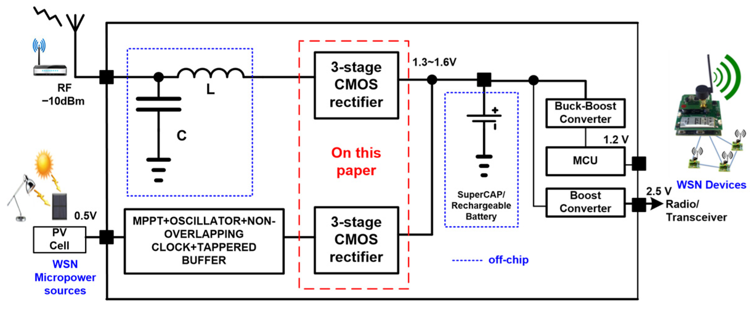
Figure 1. Block diagram of the proposed multi-stage rectifier, including its energy scavenging sources and WSN applications.
Jsan 14 00117 g001
Figure 2. Overview of multi-stage rectifier architectures: (a) traditional CCDD configuration [23]; (b) dual-path scheme using low- and high-VTH transistors [26]; (c) self-biased design [17]; and (d) body-driven technique [25].
Jsan 14 00117 g002
Figure 3. 1st stage bisection of the standard CCDD rectifier: (a) biasing profile, (b) charge phase, and (c) discharge phase.
Jsan 14 00117 g003
Figure 4. Three-stage CCDD rectifier design featuring capacitor coupling and auxiliary MOS elements.
Jsan 14 00117 g004
Figure 5. 1st stage bisection of the proposed three-stage CCDD rectifier: (a) bias network, (b) charge phase, and (c) discharge phase.
Jsan 14 00117 g005
Figure 6. Proposed rectifier featuring auxiliary pathways: (a) first stage schematic, (b) analysis, including the auxiliary PMOS device.
Jsan 14 00117 g006
Figure 7. Simulated comparison of alternative two-stage rectifier topologies at 2.4 GHz under a 100 kΩ load: (a) output voltage Vout; (b) PCE.
Jsan 14 00117 g007
Figure 8. Indoor light energy harvesting unit block diagram [29].
Jsan 14 00117 g008
Figure 9. DC-Pulsating signal conversion circuit blocks and waveforms: Bootstrapped ring oscillator, (a) schematic, (b) post-layout waveform (16 MHz), (c) chip measurement waveform (12.5 MHz); Non-overlapping clock: (d) schematic, (e) post-layout waveform (16 MHz), (f) chip measurement waveform (12.5 MHz); Tapered buffer: (g) schematic, (h) post-layout waveform (16 MHz), (i) chip measurement waveform (12.5 MHz).
Jsan 14 00117 g009
Figure 10. Parametric study of the indoor light EH rectifier: (a) output voltage versus capacitance, (b) PCE versus capacitance, and (c) PCE versus transistor size. Note that x is the ratio between Cp and Cs1a_b, Cs1a = Cs1b = 6 nF, Cp = 30 nF, CL = 1 nF, (W/L)n = 1.6 µm/0.2 µm, and (W/L)p = 4.8 µm/0.2 µm.
Jsan 14 00117 g010
Figure 11. Parametric evaluation of the 2.4 GHz RF energy harvesting rectifier: (a) output voltage vs. input power, (b) PCE vs. input power. Parameters: Cs1a_b = 70 fF, Cp = 0.7 pF, CL = 5 pF, (W/L)p = 6 µm/0.2 µm, (W/L)n = 2.2 µm/0.18 µm. Input power is referenced to 50 Ω; voltages denote peak values.
Jsan 14 00117 g011
Figure 12. Die micrographs of the fabricated rectifiers: (a) proposed indoor light rectifier, (b) conventional indoor light version, (c) standard 2.4 GHz RF rectifier, and (d) proposed 2.4 GHz RF rectifier.
Jsan 14 00117 g012
Figure 13. Measurement setup for evaluating the standalone 2.4 GHz rectifier.
Jsan 14 00117 g013
Figure 14. Measurement set-up of the rectifier for the indoor light PV-EHU.
Jsan 14 00117 g014
Figure 15. Sample measured ripple voltage snapshot of the proposed indoor light rectifier at 600 Ω. load, CL = 5 nF.
Jsan 14 00117 g015
Figure 16. Sample measured snapshot from the instrument of the proposed vs. conventional rectifier at 12.5 MHz indoor light at Vin = 0.5 V, RL = 600 Ω, CL = 1 nF, and f = 12.5 MHz.
Jsan 14 00117 g016
Figure 17. Measured and simulated output voltage: (a) indoor light rectifier with RL = 600 Ω and CL = 5 nF; (b) 2.4 GHz RF rectifier with RL = 50 kΩ and CL = 5 pF.
Jsan 14 00117 g017
Figure 18. Measured and simulated VCR: (a) indoor light rectifier, (b) 2.4 GHz RF rectifier.
Jsan 14 00117 g018
Figure 19. Measured versus simulated PCE and output voltage: (a) indoor light rectifier at VIN = 0.5 V; (b) 2.4 GHz RF rectifier.
Jsan 14 00117 g019
Table 1. List of main symbols and abbreviations used in this work.
SymbolDefinition
VINInput signal (peak amplitude)
VPPPeak-to-peak input voltage
VDCNDC output voltage at the final stage
VTHThreshold voltage of MOS transistor
VDN, VDPVoltage drops across NMOS and PMOS devices
VDROPTotal forward voltage drop, VDN + VDP
RDS_ONON-state drain–source resistance
CP, CSPumping and storage capacitors
VauxAuxiliary voltage generated by the PMOS-diode path
VCRVoltage Conversion Ratio, VOUT/VIN
PCEPower Conversion Efficiency, POUT,DC/PIN,AC
βTransconductance parameter µCox(W/L)
mDevice multiplicity (number of parallel fingers)
NNumber of rectifier stages
Disclaimer/Publisher’s Note: The statements, opinions and data contained in all publications are solely those of the individual author(s) and contributor(s) and not of MDPI and/or the editor(s). MDPI and/or the editor(s) disclaim responsibility for any injury to people or property resulting from any ideas, methods, instructions or products referred to in the content.