Abstract
Microwave Doppler sensors are used extensively in motion detection as they are energy-efficient, small-size and relatively low-cost sensors. Common applications of microwave Doppler sensors are for detecting intrusion behind a car roof liner inside an automotive vehicle and to detect moving objects. These applications require a millisecond response from the target for effective detection. A Doppler microwave sensor is ideally suited to the task, as we are only interested in movement of a large water-based mass (i.e., a person) (FMCW Radar also detect static objects). Although microwave components at are now relatively cheap due to mass production of other Industrial Scientific and Medical application (ISM) devices, they do require tuning for temperature compensation, dielectric, and manufacturing variability. A digital solution would be ideal, as chip solutions are known to be more repeatable, but Application-Specific Integrated Circuits (ASICs) are expensive to initially prototype. This paper presents the first completely digital Doppler motion sensor solution at , implemented on the new RFSoC from Xilinx without the need to up/downconvert the frequency externally. Our proposed system uses a completely digital approach bringing the benefits of product repeatability, better overtemperature performance and softwarisation, without compromising any performance metric associated with a comparable analogue motion sensor. The RFSoC shows to give superior distance versus false detection, as the Signal-to-Noise Ratio (SNR) is better than a typical analogue system. This is mainly due to the high gain amplification requirement of an analogue system, making it susceptible to electrical noise appearing in the intermediate-frequency (IF) baseband. The proposed RFSoC-based Doppler sensor shows how digital technology can replace traditional analogue radio frequency (RF). A case study is presented showing how we can use a novel method of using multiple Doppler channels to provide range discrimination, which can be performed in both analogue and in a digital implementation (RFSoC).
1. Introduction
Doppler sensors are normally used in applications where motion detection is required [1,2]. For example, they are used as interior motion sensors for automotive intruder alarms. Compared to ultrasonic systems, they have an advantage of being able to be hidden behind non-reflective materials, for example, the roof liner of a car. They can also be used in other applications, such as heartbeat sensors, as using microwave, they can penetrate the skin. One big advantage of a Doppler sensor is the speed of reaction compared to a Frequency-Modulated Continuous Wave (FMCW) Radio Detection and Ranging (Radar) sensor. The disadvantage of a Doppler sensor is its false detection probability due to the lack of angle awareness and true distance of a moving object, for intruder detection, although postprocessing Digital Signal Processing (DSP) techniques can be an aid much easier to implement using a digital-based design [3]. The purpose and significance of this work is to compare new digital FPGA-based RF technologies against traditional analogue RF. For the digital RF solution, the proposal adopts the new Xilinx’s RF System on a Chip (SoC) to implement a completely digital Doppler motion sensor. On a traditional analogue implementation, the received signal is mixed down to an IF baseband where we make sure that it is coherent with the transmitted carrier [4].
The Xilinx RFSoC devices are a new class of integrated-circuit architecture for the communications, sensors, and instrumentation markets. The RFSoC is combined with high-accuracy Analogue-to-Digital Converters (ADCs) and Digital-to-Analogue Converters (DACs) operating at gigasamples per second (Gsps), with programmable heterogeneous compute engines. The RFSoC from Xilinx has all the building elements for us to implement the Doppler sensor digitally without the need to upconvert the transmitted signal and downconvert the received signal externally. This new technology has been coined ‘RF Softwarisation’ [5].
The contributions of our work are summarised below:
- We propose a novel but efficient and easy-to-utilise Continuous-Wave (CW) RFSoC digital microwave Doppler motion sensor [6] framework implemented on the RFSoC without the need to externally pre-up- and downconvert the RF, leading to an improved performance.
- To achieve high accuracy detection for Doppler return measurements, we propose a digital decimation instead of an external mixer by extending the RFSoC hardware ‘decimation’ with soft decimation filters.
- We demonstrate how the new digital advancements in RF can provide several advantages over the traditional analogue methods in the ISM frequency band.
- The sensor trigger response to a motion event is near instant, with a low false alarm rate to non-motion events.
- The proposed sensor is coupled with a bespoke patch antenna, designed to give a quasi-hemispherical beam shape.
The rest of this paper is organised as follows: The Doppler baseband processing is presented in Section 2. The RFSoC implementation is described in Section 3.3. Experimental results are presented in Section 5. A dual-antenna case study is presented in Section 6. Concluding remarks are given in Section 7.
2. Current Context
Most Doppler microwave sensors are implemented using a simple concept of a microwave transceiver to detect moving objects in the immediate vicinity or inside an area. In order to achieve this reliably, amplitude threshold detection is used to provide positive discrimination on the basis of size or range of the target. The disadvantage of such systems is that large targets at distant range can produce a signal that is capable of crossing the amplitude threshold level of a sensor set to detect smaller targets at close range, for example, an arm moving into a vehicle through a window. As all Doppler Radar systems are only sensitive to moving targets, and the range of Doppler frequency to which the sensor can respond is severely limited by filtering, only slowly moving large targets outside the area, e.g., outside of a car body would represent a problem.
Another problem with RF Doppler sensors is the rejection of external spurious signals, such as those from microwave ovens and mobile phones. Such signals from microwave ovens can be problematic as they operate on the ISM band [7], hence why the RF electronics in an analogue system such as the mixer design have to be investigated carefully to avoid interference from anything else using the ISM band. As our proposed system is digital, we can filter these signals out providing that they are not too close to the carrier frequency. If interference is an issue, we hop the carrier to a safe frequency within the ISM band. This is relatively simple on a digital system but more complex on an analogue system. Doppler sensing is good for movement detection and the rejection of non-movement events.
2.1. Doppler Effect
First defined by Christian Andreas Doppler in 1842 [8,9], the Doppler effect is the apparent change in frequency that occurs when an object is moving radially in relation to a wave source. In case of the wave propagating in a medium, the velocity is measured relative to the medium, and as a result, the Doppler effect is dependent on the movement of both the reflective object (e.g., a human) and the source (the microwave sensor). If the moving source emits waves with frequency , then a stationary object/observer detects waves with the following frequency:
where is the propagation speed of the waves in the medium, and V is the radial velocity of the source relative to the observer. The difference between f and is called the Doppler shift frequency and can be expressed as:
Combining the previous two equations and approximating for small velocities we can rewrite the Doppler shift frequency as relative to the medium, as shown in Equation (3) below:
From the difference in frequency of the target return, the speed of the target can be calculated by means of the Doppler shift frequency.
2.2. Doppler Return
In theory, a mixer is used to look at a sinusoidal signal from a Local Oscillator (LO) (DAC-generated Direct Digital Synthesis (DDS) output in the case of the RFSoC) mixed with the Doppler return, which is the reflection of the moving target. The electric field of a transmitted wave is calculated by:
The returned electric field back at the sensor, at some later time, is calculated by:
We can then calculate the time it took to travel:
where r is the reflected return. For detecting human movement at a frequency of , the typical Doppler frequency of interest is , which equates to 0.3 to 50 ms, where is the frequency shift in hertz. Thus, in fact, only a very small fraction of a complete Doppler frequency cycle is contained within one cycle of the return signal, the rest of the signal is the envelope phase shift in time, which can be related to the radial velocity by looking at a phase vector as shown in Figure 1.
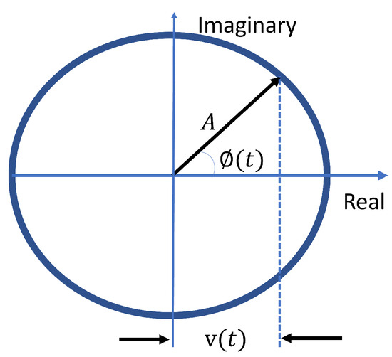
Figure 1.
Phase vector—used to provide a high resolution of the Doppler return by combining the frequency and phase shift of a Doppler return.
2.3. Phase Vector
As there is a time delay between the transmitted and received signals from the reflected object, there is a phase difference for detected moving objects. The theory is that we are observing a Doppler shift (discussed previously in Section 2.1), but as the frequencies are so low, we also see the effect of an angle-modulated sinusoid as well as the true Doppler. A mixer (for digital systems, a ‘coarse mixer’) is normally used to demodulate the phase or extract phase information. We can calculate the phase using a phase vector (phasor) [10].
In physics and engineering, a phase vector phasor is a representation of a sine wave whose amplitude (A), phase (), and frequency () are time-invariant. We can think of the phasor as a rigid rotating member of length A, making an angle with the real axis. Since the phasor rotates, is a time-variant, the (t) sinusoid wave is generated as the real part of the phasor (the horizontal projection of the rotating member), so that:
We can use the phase difference from the carrier to detect the direction ().
where is our transmitted carrier, and is the reflected return. ’s negative values are objects moving towards the antenna, and positive values are objects moving away. The phase vector should be synchronous with the carrier frequency.
2.4. Synchronous Detector
In a synchronous or coherent detector, the incoming signal is mixed with the original carrier frequency (which is the sinusoidal signal generated by the LO or DDS). The high-frequency component can be filtered off leaving only the original modulation signal. Being coherent with the carrier frequency is important for looking at the Doppler returns, otherwise we lose the Doppler information. The proposed digitally implemented mixer can be used as a synchronous detector, much like the Homodyne and Synchrodyne [11] receivers, which are systems of demodulation for amplitude-modulated or phase-modulated signals. The Synchrodyne approach is closer to our system as it uses one oscillator. The main difference is that we are not demodulating the Amplitude Modulation (AM), but instead using the phase modulation of the return signal, compared with the sinusoidal signal generated by the oscillator. For this, we need to have a stable carrier frequency. If the frequency is not exact, the entire baseband signal will be shifted by the difference. In an analogue system, this frequency shift can be observed by pulling the LO with high-return signals. The main advantage of such a method of processing, proposed in 1934 by E.G. Momet (synchronous detection) [12] is the high selectivity of reception for weak radio signals on a noisy background, giving an improved SNR. The demodulator is what is termed a coherent modulator, as it only sees the components of noise that are in phase with the LO. Consequently, the noise level is reduced and the SNR is improved.
On a traditional analogue Doppler motion sensor, the RF front-end section consists of a mixer, oscillator, power splitter, and antennas. The analogue electronics takes the mixer output, which is then filtered and amplified onto a baseband. Power splitters are used to split the power output of the oscillator between the antenna path and the LO, whereas for the proposed solution, this processing chain is performed digitally on the chip.
3. Proposed Solution
The proposed solution was to implement a complete analogue chain for a Doppler motion sensor digitally on a Xilinx RFSoC device as a single-chip solution, without the need to externally up- and downconvert the transmitted and received frequencies. For a digital implementation, the techniques are completely different. For the digital RFSoC implementation, the transmitted signal was generated using a DDS and DAC via a reconstruction filter (this removed the high-frequency contents) connected to a balanced to unbalanced device (BALUN), then finally the antenna. Note that the DACs had a mixing microarchitecture and used a Digital Upconverter (DUC) to place the carrier information in Nyquist zones 1, 2, and 3 taking the possible frequency range to the end of the C-band. The input was from the receive antenna and fed directly into the ADC via a matched transmission line.
3.1. Transmitted Signal
For the transmitted carrier frequency, it should be centred in the ISM band, around . What we did not want was to create frequency spurs or transmissions or transmit where there was interference. In the PYNQ spectrum analyser mode in Figure 2, we could check for interference [13,14]. If there was is, say from a microwave oven or Wi-Fi, we then moved the transmit frequency (with the aid of the Xilinx RFSoC Frequency Planner as shown in Figure 3) until the spurious frequencies’ Spurious-Free Dynamic Range (SFDR) was below −80 dbm, making sure that we still were in the ISM band. One method of reducing the spurs is to apply phase dithering (or Wheatley jitter [15]) to reduce amplitude quantisation noise and improve the SFDR of the Numerically Controlled Oscillator (NCO). A phase dither generator is basically a random-integer generator used to improve the oscillator’s output purity, using the spare bits from the integer conversion. Dithering causes the unintended periodicities of the quantisation noise to be instead spread across a wider frequency band, effectively reducing these undesired spurs. The conservation of energy applies, resulting in raising the overall noise floor above the electrical noise. On the plus side, this can reduce the SFDR by up to 12 dB. The DDS-generated carrier frequency settings were set using the Xilinx RF data converter’s Intellectual Property (IP) block as shown in Table 1 and Figure 4. Interpolation rates were set to 2× (with greater than −89 dB image rejection), doubling the frequency.
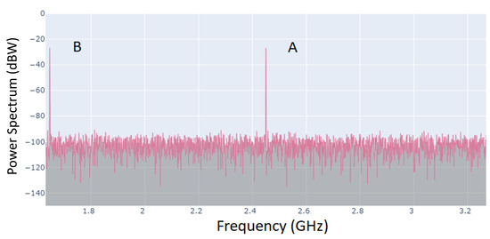
Figure 2.
Spectrum analyser (RFSoC) PYNQ software framework (frequencies up to 4.096 GHz using higher-order Nyquist zone techniques) [13], showing (A) carrier and (B) fold of the carrier into the 1st Nyquist zone.
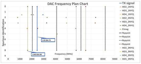
Figure 3.
The Xilinx RFSoC Frequency planner setup for the ‘TX carrier signal’ (in blue) at , showing an image in the 1st Nyquist at . This is confirmed in Figure 2, where we see the carrier and fold on the proposed sensor’s RF output (HD = harmonic distortion; dotted lines denote Nyquist zones (NYQ)).

Table 1.
RF hardware block parameters’ settings sampling at , under Vivado.
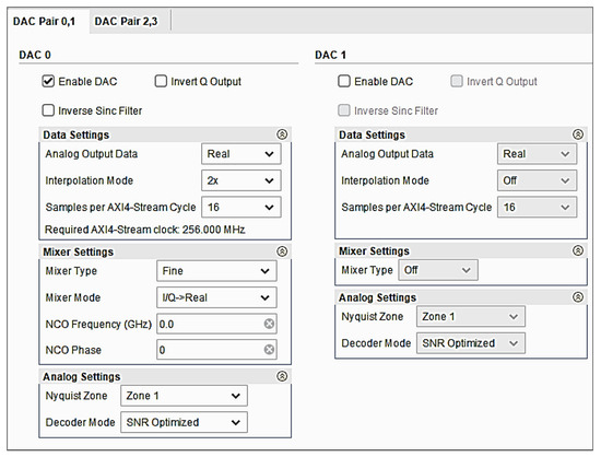
Figure 4.
Xilinx RF data converter’s IP block—DDS-generated , from the onboard 6 Gasps DAC.
The DDS-generated signal was then transmitted via an antenna (after the BALUN). For the antennas, we used a patch antenna design, with a SubMiniature version A (SMA) feed. Microstrip or patch antennas are the cheapest solution as they can be printed directly onto a circuit board, making them easy to produce. In Figure 5, we show the design for the proposed patch antenna, which is fed by a microstrip transmission line. The patch, microstrip, and ground plane were made of high-conductivity metal, e.g., copper. The patch was of length L, width W, and sat on top of a substrate, such as FR4 or Rogers. The substrate had a dielectric constant and thickness H. The ground plane was at the bottom of the board. The thickness of the ground plane or of the microstrip copper layer had little effect on the antenna performance, therefore we could create a beam shape that was suitable for motion detection, inside a confined area. The receive antenna was connected to the input filter, a Mini-Circuits VBF-2435+ with a frequency range from 2340 MHz to 2530 MHz. To increase the receive sensitivity, we used a NooElec low-noise variable gain amplifier (30 MHz to 4000 MHz), although this was optional.
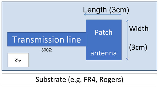
Figure 5.
Patch antenna design for the transmit and receive modes. ( = dielectric constant of about 4.5). The width W of the antenna controls the input impedance (300 ). By increasing the width, the impedance can be reduced. However, to decrease the input impedance to 50 requires a very wide patch [16] (90 mm for RF4 at ).
The frequency of operation of the patch antenna, as shown in Figure 5, is determined by the length L. We can calculate the centre frequency by using Equation (9):
where ms−1 represents the speed of light, dielectric constant, is the permeability of vacuum, and is the permeability of air.
With Equation (9), we can show that the patch antenna should have a length equal to one half of a wavelength within the dielectric (substrate) medium. Our antenna was 30 mm × 30 mm using RF4, tuned for , as shown in Figure 5. The width W of the antenna controls the input impedance. For a square patch fed in the manner above, the input impedance is of the order of 300 . By increasing the width, the impedance can be reduced. However, to decrease the input impedance to 50 s often requires a very wide patch (90 mm for RF4 PCB material). The width further controls the radiation pattern, which is important for our range discrimination scheme. The proposed patch antennas give a quasi-hemispherical radiation pattern as shown in Figure 6.
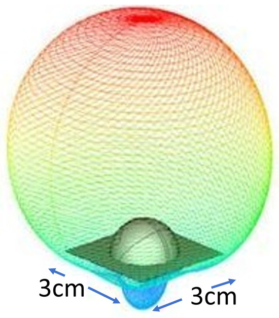
Figure 6.
Hemispherical radiation pattern plot taken from the proposed patch antenna.
3.2. Received Signal
From the ADC, the sensor receives the reflected return. To compute the frequency resolution required, we first calculated the wavelength: = , where c = speed of light and f = frequency. This meant a value of cm was equal to one wavelength at . For a finer resolution (less than 12 cm), we used the phase (as discussed in Section 2.3), which resulted in a resolution of 3 cm if the wave was divided in 4 quadrants (this can be performed digitally using a coarse mixer) [17].
The next step was to downconvert and filter digitally. In the analogue system, a power splitter was used to pass power from the transmitted signal to a mixer. (The Wilkinson power splitter was first demonstrated around 1960 by an engineer named Ernest Wilkinson [18], hence the name.) For the digital implementation, the translation of the bandwidth of interest to the RF carrier frequency was achieved by digital mixing as shown in Figure 7 (This was possible on the RFSoC, as the ADCs are capable of sampling up to 4 gsps, hence we could directly sample the input without the need to externally mix down the signal). The frequency source signal from the ADC was mixed down with the complex NCO to baseband. The fine mixer used a 48-bit NCO, with programmable frequency and phase components. The NCO may be seamlessly updated at run-time to allow for fine-tuning and to be in phase with the transmitted frequency. From the frequency planner, the receive signals were in the second-order Nyquist zone and produced an image at in the first Nyquist zone as shown in Figure 3. Being digital, if centred and sampled at the lower frequency from the image in the first Nyquist zone, then more sample points are gained, giving less spurious frequency readings. As the Doppler frequency range was in the order of 100 Hz (typical human walking movement generates Doppler shift just below 100 Hz), there was a need to decimate to obtain the resolution as discussed in Section 3.5. As we were downsampling, we lost the resolution in frequency but maintained the phase. We could recalculate the frequency shift by adding back the phase difference at the end of the chain.
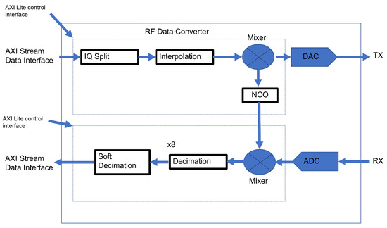
Figure 7.
High-level diagram of the RF DACs (top) and ADCs (bottom).
In the case of an FMCW Radar, constructing the Doppler shift can be performed by matching the peaks taken on the up-ramp in time, then comparing them with the peak points on the down-ramp [19]. In the case of a microwave motion sensor, it only has the Doppler return, which consists of phase and frequency shift plus the power level of the received signal, compared with the transmitted signal. One method of processing the Doppler shift frequency from any reflected return signal is to use a Fast Fourier Transform (FFT) [20]. An FFT was performed on the mixer/decimation output, recording the frequency plus phase difference and amplitude in a rolling buffer. This allowed the visualisation of the Doppler return as shown in Figure 8, with the amplitude shown as either the power level or phase shift (shown as colour intensity). The distance can be calculated by the amplitude (power level), but for an accurate figure, the system would need to know the size of the reflecting object, which can be an issue.
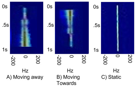
Figure 8.
(A) Metal plate moving towards the antenna at walking pace, from a distance of 3 m, (B) and away from RFSoC antenna. (C) The frequency remains constant when there is no motion detected (taken in UoL’s anechoic chamber).
3.3. Proposed RFSoC FPGA Design
Xilinx Sysgen under Mathwork’s Simulink was used to simulate and generate the simulation and the main IP block. Where Sysgen’s IP blocks could not be used, bespoke VHDL/Verilog code operated as a black-box block. The Xilinx Vivado was used for the synthesis. The Sysgen block diagram of the proposed system in Figure 9 consisted of the transmitted frequency DDS, which was centred at . A digital mixer block mixed the transmitted signal with the returned signal. This in turn used a decimation block (with finite impulse response (FIR) filters [21]), to obtain our IF band of interest. The FIR filters used a parallel polyphase structure with systolic subfiles, as used by the LogiCORE FIR Compiler [22]. These were mapped to a specialised DSP48E2 multiply-accumulate via the Super Sample Rate (SSR) blockset. These SSR structures can exploit coefficient symmetry. Then, finally, an FFT block produced the Doppler returned frequency, which went to the rolling buffer in memory. Note that SSR vectors allow running the blocks in parallel, obtaining the throughput rate required on the Programming Logic (PL) fabric, with a low clock rate. The FFT of the decimation block made a zoomed FFT, which was required as it was not possible to apply the FFT on the returned signal over the whole spectrum. This is an effective known technique used for improving the spectral resolution of the FFT without increasing the FFT length, N. This technique reduces the sample frequency of the time-domain signal. In this case, our research used the mixer approach, which mixed the signal with the transmitted carrier frequency, then applied a downsampling low-pass filter to reduce the overall sampling frequency. The mixer approach initially shifted the frequency band of interest to DC. The FFT was applied to the decimated signal. Since the sample frequency was reduced, the overall spectral resolution improved.
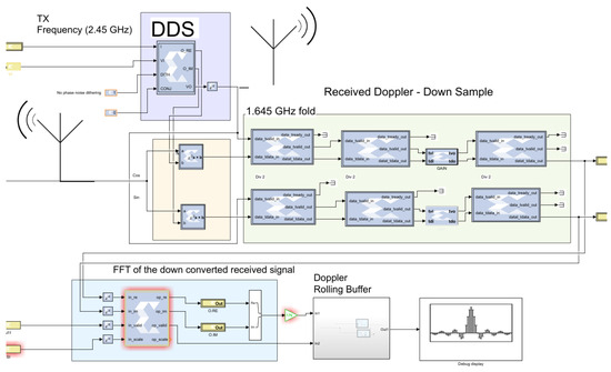
Figure 9.
Top Level diagram of the RFSoC-based Doppler motion sensor: implementation in Matlab Simulink using Sysgen. Note that the design is synthesised under Xilinx Vivado for the XCZU28DR-2E RFSoC.
3.4. Phase-Noise Considerations
Direct-RF data converters have seen increased adoption in remote-radio head TX and RX, due to their unparalleled bandwidth and flexibility. However, since these converters need to directly synthesise and sample multi-GHz radio signals, the sampling clock must exhibit excellent phase-noise performance to minimise self and adjacent channel mixing, and strong suppression of reference and harmonic spurs to meet stringent out-of-band emissions and minimise aliased energy. We recorded the phase noise on a Rohde Schwarz ©FSWP phase-noise analyser, and even though we were using two low-cost clock crystals, at 12 MHz and 122 MHz, we recorded phase noise of less than 110 decibels relative to the carrier (dBC) at 1 KHz (shown in Figure 10). This compared to the , using the integrated RF data converter’s 7.4 to 14 Phased-Locked Loop (PLL) [23], giving −120 dBC/Hz at 100 KHz. The excellent performance was partly due to the onboard LMK04832 ultralow-noise clock jitter cleaner with dual-PLL chip from Texas Instruments and the fact that silicon-based DACs, by their nature, exhibit good phase performance.
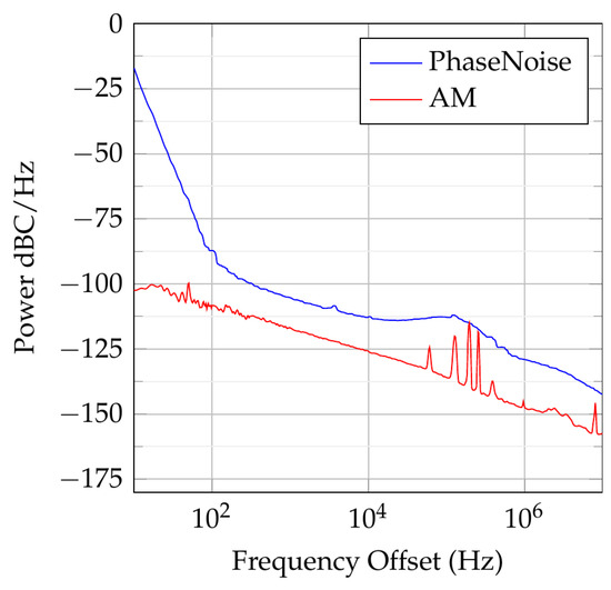
Figure 10.
Recorded phase noise for , taken on an R&S©FSWP phase-noise analyser and Voltage-Controlled Oscillator (VCO) tester [23] Note that the non-linearity at the frequency offset of is due to the effect of the PLL charge pump [24].
3.5. Signal Decimation
In order to achieve high accuracy detection for Doppler return measurements, we only needed to apply an FFT on the carrier minus the received signal, which contained the Doppler information. Traditionally, this is achieved by mixing the carrier with a lower frequency, but here, we used the NCO. For the proposed solution, we decimated the periodic portion of the ADC samples of interest, while ignoring the rest (digital version of mixing). Decimation is the process of reducing the sampling rate by low-pass filtering a signal digitally. A maximum signal decimation factor of 8 can be implemented in the FR-ADC block (no PL resources taken), with greater than −89 dB alias rejection. As the Doppler return is in Hz, this is not enough. To increase the decimation factor further and the corresponding spectral resolution, we implemented additional soft blocks in the RFSoC’s PL [25]. A simple approach is to implement a cascade of half-band decimation filters in the RFSoC’s PL. They were implemented by three stages of 2× half-band FIR filters. These implemented the analysis portion of a two-band filter bank to filter a signal into low-pass and high-pass sub-bands, with each stage optimised to preserve up to 80 percent of the signal bandwidth. From this, we could achieve an FFT resolution of kHz. As the frequency was too high for the Field-Programmable Gate Array (FPGA) to process on the PL, we packed this into vectors. The packing of samples in vectors, is known as the Super Sample Rate SSR, which can be between 1 and 8 samples per clock cycle. The SSR factor is based on the following formula (where D is the FPGA Programming Logic’s clock frequency of 200 MHz, and is the sampling frequency):
In the proposed system, we used the FIR compilers in Sysgen [26] to set the low-pass filter. From Sysgen, we created our IP block, for integration into a Vivado block diagram. In the block diagram, the data collector block was used for communication with the RF ADCs and DACs [27]. The transmitter block set up the output transmit frequency ( ) carrier. The received block contained 1 channel 00 which connected to our decimation core.
The output after mixing, decimation, and filtering was then processed by an FFT, to obtain our Doppler frequency, which we then recorded in a rolling buffer on the Advanced RISC Machines (ARM) core. If we view the rolling buffer, we see the Doppler return just as we would in the baseband of the analogue system. In Section 2.1, it was shown that the Doppler shift frequency was proportional to the sensor and the speed of the moving object. Once the Doppler shift frequency wasted, the final step was to find the distance/position. Integrating the speed with respect to the discrete time achieved this.
Finally, we added an alarm trigger based on the Doppler shift and amplitude from the return signal. From data stored in our rolling buffer, we applied our trigger level to determine an alarm event. To improve the false alarm rate, we added a digital charge pump. A digital charge pump adds a value when the Doppler shift frequency is above a threshold, otherwise a value is subtracted. In analogue electronics, this is called a charge pump. When testing/setting up the sensor, the settings for the charge pump can be altered. The charge pump should only increase if the detected signal is above the noise floor, which is a level set by the user.
3.6. Noise Gate Filter
The baseband contains a noise component, though it has a much lower power than the signal component. The problem is when there is no signal (i.e., when the sensor has no movement to detect), there is still noise that disturbs the Doppler shift estimations. This is because the frequency estimators do not consider the amplitude of the signal, only the frequency distribution. In sound engineering there is an electronic filter device known as a Noise Gate (NG) [28]. This only passes the signal through if the energy is above a certain threshold. That way, the low-power noise is eliminated when there is no other high-power signal. The same idea can be used in our case. When there is no Doppler, the signal is ignored. The level can be set by recording the baseband level in a small anechoic chamber. We can call this level our noise threshold. In fact, a standard microwave oven is ideal as an anechoic chamber as it was designed for operating at .
3.7. FFT Alternatives
Processing DSP algorithms such as FFT on hardware is resource-intensive. Since we used an FPGA for processing, the ideal method of processing a Doppler return would be if we could process without using an FFT, which would reduce the response time as the signal is integrated over time. One scheme of interest is the Boyer method [29] as this looks at the zero crossings of the signal. The estimation of the frequency content in a signal can be performed by counting the number of zero crossings per unit time. This method is suited to a digital system. A pure sinusoidal signal has two zero crossings per period, and the frequency is directly proportional to the number of zero crossings per unit time. In Section 2, it was shown that the Doppler shift frequency was proportional to the sensor and the speed of the moving object, which could be calculated using the zero-crossing technique. The zero-crossing counting method is handled differently as the estimation of the travelled distance can be calculated from the baseband signals, without first calculating a speed estimate.
4. Experimental Setup
For our research, the RFSoC 2 × 2 development board from GlobalTech as shown in Figure 11 formed the base platform for the proposed motion sensor [30]. The RFSoC chip was the XCZU28DR-2E device from Xilinx, which is referred to as the RFSoC in this paper. In the Processing System (PS), there is an Application Processing Unit (APU) which houses an Arm Cortex-A53 MultiProcessor Core (MPCore) consisting of four Central Processing Unit (CPU)s.
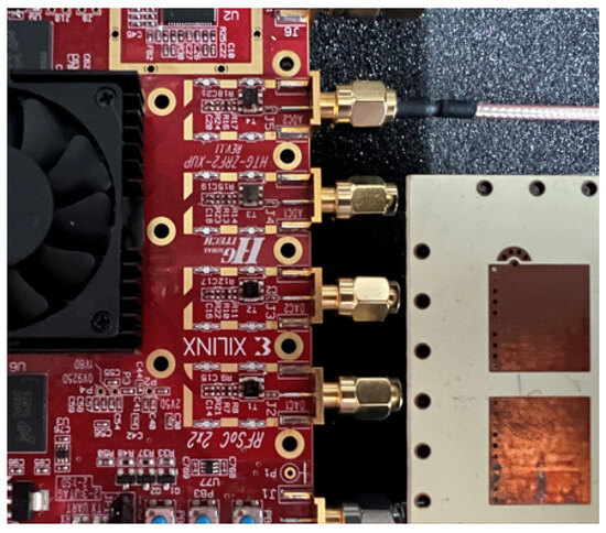
Figure 11.
RFSoC 2 × 2 development board from GlobalTech, connected to a patch antenna.
The PL contains the Kintex UltraScale + FPGA logic fabric, which includes both RFADC and RFDAC data converters. There are eight DACs and eight ADCs in the XCZU28DR-2E device with only two of each being accessible on the 2 × 2 RFSoC board, as shown in Figure 11. They can operate at up to 4096 Msps and 6554 Msps, respectively. The data converter’s blocks were integrated subsystems that each contained a mixer with a programmable NCO for modulation/demodulation, along with a programmable decimation filter (for the RFADCs) or interpolation filter (for the RFDACs), as shown in Figure 9. On the DAC input for the received signal, a ‘Mini circuits’ VBF-2435+ bandpass filter which passes frequencies from to was used, as we were only interested in the ISM band. The DAC SMA input was connected to an FR4 microstrip patch antenna, that was tuned for a frequency of as per Figure 5. In the case of the proposed Doppler motion sensor implementation, for a production release, only a regulated power supply, the RFSoC XCZU28DR-2E device, and a low-frequency clock (for cost) with an ultralow-jitter PLL plus a BALUN on the output is actually required. For comms, a CANbus interface can be added. This made a much smaller board than the GlobalTech 2 × 2, which was then sizewise comparable with a typical Doppler sensor, as shown in Figure 12. The actual resource usage of the FPGA was low as shown in Table 2; this was mainly due to the utilisation of inbuilt hardware block for mixing and decimation. Having an ultralow-jitter clock source was critical for low-phase-noise performance.
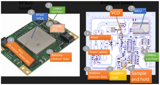
Figure 12.
(Left): Proposed RFSoC-based Doppler sensor. (Right): Typical analogue Doppler sensor. The proposed RFSoC Doppler sensor’s main components consist of a crystal/PLL, RFSoC FPGA, and BALUN. A typical analogue Doppler sensor consists of a Voltage-Controlled Oscillator (VCO), mixer, power splitter, amplifier, sample and hold (or ADC), and a Microcontroller Unit (MCU). Both designs have an antenna on the bottom side of the PCB and an optional CANbus interface. From a PCB design prospective, the analogue sensor is more complex. The typical analogue sensor does have more functional chips in the chip list, but compared with the digital RFSoC, the circuit complexity of microprocessors and others does not seem to be as high as that of RFSoC. For example, analogue sensors using the bandpass IF sampling principle only need a crystal oscillator, PLL with integrated Voltage-Controlled Oscillator (VCO), ADC with a high enough analogue bandwidth, and a low-cost Microcontroller Unit (MCU). The RFSoC presents the concept of a single-chip solution, bringing the benefit of a digital system.

Table 2.
Resource utilisation on the Xilinx XCZU28DR Zynq Ultrascale + RFSoC for the proposed design.
5. Experimental Results
In Figure 8, we showed in (A) the results of a 1 m2 metal plate moving towards the RFSoC antenna at walking pace, from a distance of 3 m, (B) away from the RFSoC antenna, and (C) that the frequency remained constant when there was motion. The results looked identical to that of an analogue system when the power level was normalised, which was good as the technologies were completely different, demonstrating that we had a working solution. From the comparisons in Table 3, we can see that our improved SNR gave us a better detection distance and sensitivity, with the RFSoC able to detect signals above 89 dBs. This was due to the analogue system requirement for a high gain amplification of the baseband, making it susceptible to analogue electronic noise appearing in the IF baseband, such as from a power supply regulator.

Table 3.
Comparative performance between the RFSoC and a typical Doppler motion sensor.
In Table 4, we performed a comparison. The comparison results include the temperature performance, field upgradability, antenna requirements, power consumption, and detection time. Being FPGA-based, time to detection was similar, but with better DSP abilities leading to reduced false detection. The advantage of using a DDS for frequency generation compared to an oscillator was that we had full control over our carrier frequency. Emissions were also good, providing we carefully selected our frequencies, avoiding spurs generated by aliasing. Digital systems are more repeatable in production, whereas analogue systems require more tuning. Unfortunately, current consumption was poor, as shown in Table 4 () although it would have been comparable if implemented as an ASIC and the RF duty cycled. In the future, we could gain more motion and distance accuracy by also looking at the phase difference as well as the frequency between the transmitted carrier and received signal. After decimation, the phase could be converted to a frequency, allowing for finer resolution as shown in the results in Figure 13. Note that we required two processing chains, one for the phase and the other for the amplitude as shown in Figure 9.

Table 4.
Feature comparison between the RFSoC and a typical Doppler sensor. RF softwarisation means that the device can be ‘hardware’-updated using software in the field, which is a big technology advancement compared to fixed analogue hardware. A single Integrated Circuit also means a smaller footprint. Current consumption is high on the proposed RFSoC sensor, although it would be comparable if implemented as an ASIC and duty-cycled.
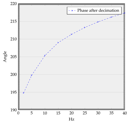
Figure 13.
After decimation, the phase information can be preserved then used to re-calculate the frequency shift. Here, we can see a reconstructed frequency shift from the preserved phase information, giving us a finer resolution otherwise achieved from just straight decimation.
During testing, it was noted that an exception to the roll-off distance rule was that objects within a large metal shell (such as a vehicle) tended to change their received amplitude from a to a law, where R is the distance from the antenna arrangement, dependent on the total field perturbed by the moving object. External objects tended to fall off with a law [31], as in the case of free space Radar for small objects. We observed the Doppler return following the to law for larger objects such as a moving metal plate.
Initial testing of the system also revealed an unexpected amplitude response at distances relatively close to the sensor. As a target approached the sensor, the Doppler amplitude would appear to rise following the expected law until approximately 10 m from the sensor. At distances below 10 m, the amplitude would suddenly appear to peak and fall at random. Further investigation revealed this behaviour to be due to Fresnel zones [32] or ‘multi-path fading’. Fresnel zones are areas in which if a radio wave is reflected back toward the source, the radio wave arrives with the same relative phase as the original wave. If the reflection arrives in phase with the original wave, the waves increase. Alternatively, if the reflection is out of phase in relation to the original, the waves cancel out. The locations of the Fresnel zones for were calculated using Equation (11):
where = reflected power, = height of target, = height of receiver, and R = range in metres. Note that all even (two, four, six etc.) Fresnel reflection zones cause a cancellation of the received voltage, whereas all odd (one, three, five, seven, etc.) zones cause a reinforcement.
6. Case Study (Using Directional Antennas)
For our case study, we used the Doppler motion sensor for the detection of intrusion into a motor vehicle. To provide, some locational information, we added an additional antenna for dual detection.
Most microwave sensors for automotive use range gating or Doppler with threshold detection. On the market, there are currently some Doppler multi-channel Radars, such as the FWM7RAZ01 from Fujitsu which is a three-channel, 24 GHz Doppler Radar sensor [33]. Others include the RFbeam K-LC6, which is a dual-channel Doppler Radar module [34]. Devices such as these use antenna arrays with the same beam shape per channel, whereas here, we used switched dual Doppler channels with overlapping antenna beam patterns and sampled the phase difference, making the application novel, which we coined ‘range zoning’. We also showed that our ‘range zoning’ could be implemented both digitally and in analogue.
To see the effects of dual detection, covering overlapping zones, the antennas needed to be duty-cycled to prevent injection locking. On an analogue system, this is performed using a sub-ns RF switch with good isolation. On an FPGA-based system, we can control this by simply turning the Transmit (TX) on and off in sync with the system clock, using the PL of the FPGA.
From the dual antenna, as well as directional information, we can gain zoning information. For an automotive application, this can be used for intruder detection, with the added benefit of detecting the location of the intruder event, i.e., the front windows of the car. Other applications include occupant detection.
6.1. Directional Antennas
The Doppler return on its own does not give any angular information [1,35]. To overcome this, we implemented multiple directional patch antennas, which we switched in and out on a duty cycle. We found that the ‘Boyer differential phase scheme’ [29] was ideal for beam shapes that were the same on both channels. As our RF overlapped the middle, we needed to add to the scheme a novel solution. From empirical observation, we added our own scheme that we named ‘Amplitude zoning and range factor’.
6.2. Distance (Using the Zero-Crossing Technique)
The zero-crossing counting method, as discussed in Section 3.7, was handled differently, as the estimation of the travelled distance could be calculated from the baseband signals, without first calculating a speed estimate. The number of zero crossings within a time window was proportional to the speed. Then, integrating the speed with respect to time was the same as summarising the zero crossings () as shown in Equation (12).
where d is the distance travelled in the time interval between and .
This technique could also be used to calculate high-speed frequencies on purely a digital system [29], as when sampling the baseband of both channels, we were interested in just the zero crossing. This technique could be simplified further by using the Boyer technique [29] of measuring the time between lead and lag of the two Doppler signals (switched antennas) from the zero crossing instead of using a window function, as shown in Figure 14, from which we could measure the difference between the two channels, giving us the directional information.
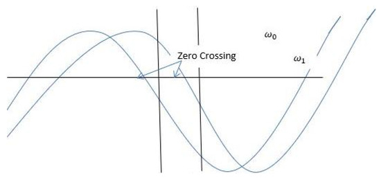
Figure 14.
Boyer technique applied to two baseband signals, from the dual-antenna arrangement. Here we see the receding target: Doppler from lags , approaching target: Doppler from leads .
6.3. Amplitude Zoning
For a given target cross-section, the amplitude of the detected signal falls off with the distance from the sensor in the far field, as previously discussed in Section 5; therefore, a large baseband signal could be interpreted as a target close to the sensor, while a small signal could represent a distant target; as an example, a “bag grab” near the sensor will have higher amplitude than one 2 m from the sensor.
This is of limited general value since the target cross-section has a large influence on the result and there is no directional information—a distant object fore and aft being at a relatively greater distance than, say, one on the side of a car. If, however, we restrict ourselves to considering genuine intrusion threats, useful limitations can be imposed on the range of signals we have to consider. We need only consider three or four target regions within our application, that of a passenger car, although in practice, we should double this number to take into account the variations between the left and right sides of the car/area.
6.4. Range Factor
As our beams did not fully overlap, we needed to add to the Boyer scheme to verify the range calculation was correct. When looking at this, it was observed that the relative amplitudes of two channels varied as the distance from the sensor changed. It was found that the distance of the target from the sensor could be estimated by comparing the amplitudes of channel A and channel B’s signals as shown in Equation (13).
where R = range factor.
This was provided that averaging was applied to the baseband signal. The optimum averaging period appeared to be 0.6 s.
Note that ranging is only one-dimensional, indicating the distance in front of or behind the sensor. In principle, R is a continuously varying function between / and , where the sign indicates whether the target is in front of, or behind the sensor. In practice, in order to implement this on an FPGA, it is preferable to use integer arithmetic. This is most easily achieved by modifying Equation (14) to:
where K is an arbitrary integer constant. By changing the value of K, we can adjust the number of range divisions along the length of the vehicle. A and B are the baseband signal voltages for the two channels. Target zones (front seats, rear seats) can be defined by a spread of a range of factors. For example, 2–5 being zone 1 (front of the car), 7–9 being zone 2 (rear of the car), etc. Plotting R against the angle gave the following chart, as shown in Figure 15 below:
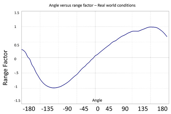
Figure 15.
Angle verses range factor—ideal conditions over the range from to .
Figure 15 shows that under ideal conditions, over the range from to , an almost linear relationship between range factor and angle is evident. This in turn translates as a simple monotonic relationship between the range factor and the distance of the target in front of the sensor i.e., we can use the relative amplitudes of the signals from the two channels to determine the position of a target along the car. Ideal conditions relate the antenna’s insensitivity to the ground plane’s environment. It should be noted that this positional information relates only to the one-dimensional distance in front of or behind the sensor. No information is available in the transverse direction.
6.5. Range Factor—Typical Environment
If the sensor were to be used inside a car, one of the issues can be that the roof of the car can be seen as a large ground plane which would cause a distortion of the beam shapes as shown below in Figure 16:
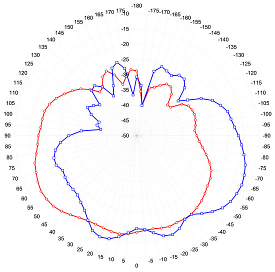
Figure 16.
Ground plane distortion caused by the roof of the car being a metal body. In blue is antenna one and in red is antenna two.
This has an effect on the range factor with the range as shown in Figure 17.
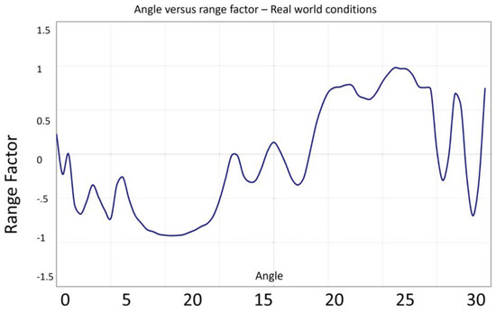
Figure 17.
Angle versus range factor—real world conditions.
Even in this extreme instance, however, we can still clearly see spatial discrimination. Whilst we may no longer be able to accurately determine the distance to a target, there are the three areas (−90 to –50, −40 to +30, and +45 to +90), which are clearly defined by a unique range of range factors. Thus, although we cannot determine where in a particular area the target is, we can localise it to one of these ‘zones’.
In practice, this is all that is required for a car alarm since the interior of a vehicle is naturally divided into zones—the front-seat area, the rear-seat area, the back-seat area (i.e., MPV and SUV’s), and the boot area. These are the areas that the sensor needs to protect, and knowing whether a target is in one of these areas or not provides significant data to determine how the sensor should respond.
6.6. Charge Pump
For each of the detection zones, we need only consider the parts of the baseband signal that occur while the target is within that zone; the signal level in all other parts can be set to zero. See Figure 18 where different colours are used to represent the different multiple charge pumps in action.
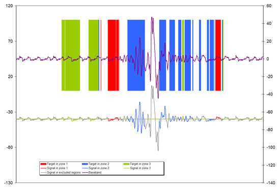
Figure 18.
Multiple charge pumps.
A standard charge pump analysis can be applied to each of these extracted baseband signals. In the example in Figure 19, where we have a bag grab from the centre row of seats, only the signal present in zone 2 is sufficiently high to exceed the charge pump threshold even though this threshold can be individually set for each zone.
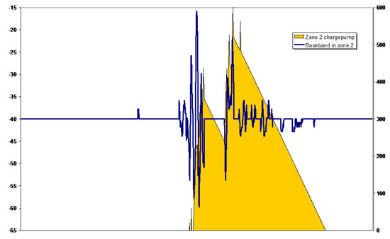
Figure 19.
Charge pump on the extracted signal as shown in yellow.
6.7. Sensitivity Zoning
Figure 20 shows a pair of sensitivity contours that could be expected for one channel of a sensor. In the case of the red (high-sensitivity) contour, the whole of the interior of the vehicle is protected, but at the cost of large amounts of leakage through the side windows. This would render the sensor very sensitive to false alarms from external targets, such as metal plates. Reducing the sensitivity (green contour) removes this problem by constraining the beam within the windows, but large areas of the vehicle (including most of the front-eat area) is left unprotected.
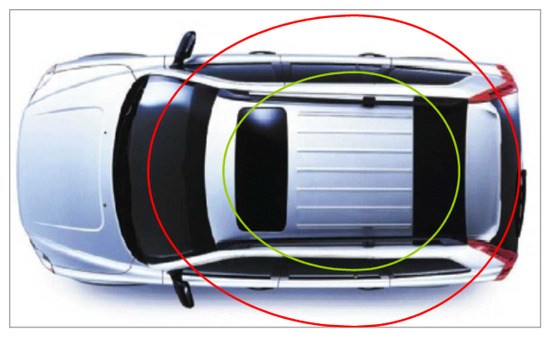
Figure 20.
Sensitivity contours for a single beam sensor. Reduced sensitivity shown in green contour and high-sensitivity contour shown in red.
In Figure 21 shown above, we used the same sensor but used range zoning to isolate three sensitive areas in the car. In the magenta zone (covering the rear- and back-seat areas), sensitivity was set to a low value to avoid leakage through the side windows. In the green (front) and orange (boot) zones, sensitivity was set to a high value for maximum detection. Side leakage was not important in these cases since the main window area did not fall within these zones.
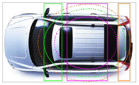
Figure 21.
Sensitivity contours when isolating three sensitive areas in the car. Magenta zone covering the rear and back seats. Green is the front and orange is for the boot.
6.8. Results
For testing, a 1 m2 metal plate was moved towards and away from the sensor. The data were then processed and plotted as shown in Figure 22, Figure 23 and Figure 24.
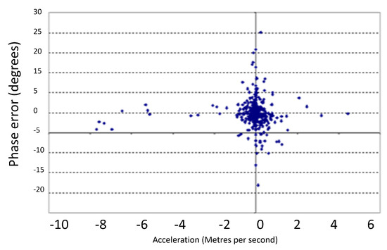
Figure 22.
Distribution of phase error with changing acceleration.
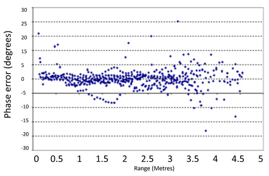
Figure 23.
Phase error against increasing range.
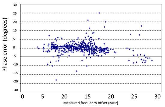
Figure 24.
Measured frequency phase error against Doppler frequency.
Figure 25 shows an example baseband of actually captured Doppler results, processed using the Boyer scheme. This implementation proved that FFT processing in the case of an analogue baseband was actually unnecessary and the zero-crossing counting scheme could be used to acquire frequency information without the overhead of running an FFT.
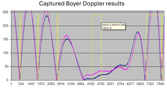
Figure 25.
Captured Boyer results. The blue channel is the Doppler return from antenna one and the magenta is the Doppler return from channel two. The yellow trace is the processed ‘Boyer’ channel.
It was also observed that phase errors were introduced at different target speeds, particularly during acceleration and deceleration. Rejection of these errors was achieved by measuring variations in Doppler frequency from the expected centre frequency of 10 . Figure 26 shows the result of a 1 m2 metal plate manually moved towards and away from the sensor.
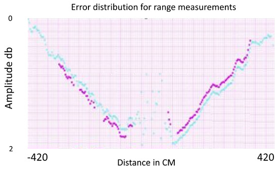
Figure 26.
Boyer scheme tested with a 1 m2 metal plate manually moved towards and away from the sensor. In blue is the Doppler return from antenna one and in magenta is antenna two. Both channels are plotted against distance and speed (where the amplitude is used for the distance, and frequency/phase change relates to the speed of travel).
The various plots show the test results achieved with the Boyer scheme. Figure 22 is the distribution of the phase error with changing acceleration. Some vertical distribution of the phase error around the constant velocity, the zero-acceleration point, was noted; this may have been due to uncertainty in the operation of the prototype software, due to spike noise. However, the majority of the 495 measurements were very well correlated, and more importantly, showed little sign of divergence in terms of phase error with increasing acceleration.
Figure 23 shows the phase error against the increasing range. Convergence was tightly packed out to about 2 m with increasing scatter after that point, due to the falling amplitude of the signal with the range. Figure 24 shows the phase error against the Doppler frequency. Again, the distribution was good, showing good correlation between 4 and 20 .
Figure 27 shows the distribution of range error in the measurement set. This was again very encouraging for a simple sensor of this type, operating at a low microwave frequency and with a low deviation. The above results are a clear indication that the ‘dual antennas’ worked well, but with the proviso that some refinement of the software is necessary to improve the occurrence of ‘widows and orphans’ in the measured data. The sensor gave an output proportional to the range over a wide range of Doppler frequencies and accelerations, and out to a range in excess of that required for a car motion sensor. It could also distinguish between an approaching or receding target, which is ideal for the Thatcham bag snatch test. Thatcham [36] is a testing standard used in the automotive industry, to meet standards set by insurance companies.
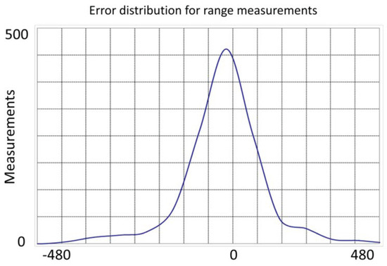
Figure 27.
Error distribution for 500 range measurements (10–480 cm).
6.9. Case Study Conclusion
From the literature search, as discussed, the scheme for detecting distance and speed that was of most interest and best suited to an RFSoC FPGA implementation was the Boyer scheme using the zero-crossing method on our generated Doppler baseband. The main issues with the Boyer scheme were that although it was providing directional and distance information, it still did not tell us if the location of the movement event was to the left or right, and it would require some processing from an additional antenna. The scheme was suited to running on an FPGA, as the FPGA can process multiple antennas’ return signals in parallel and provide sub-nm resolution, due to the fast clock rate. It also demonstrated that an additional antenna could be added to the RFSoC (as up to four ADC and DAC channels are supported by the RFSoC), which is complicated to do on a analogue-based system.
7. Conclusions
It was shown that a Doppler motion sensor could be implemented digitally on an RFSoC without the need to externally up- and downconvert, providing we used Nyquist zones and preserved the phase information. Mathwork demonstrated a pulse Doppler Radar [37], using the higher-end ZCU111 RFSoC, which is the nearest known equivalent. The main difference being that the Radar was pulsed compared to the proposed CW Radar. Here, we demonstrated a CW Doppler motion sensor that could be implemented on all variants of the RFSoC. The RF SNR performance was found to be superior compared with a typical analogue system, but the power consumption was too high (Table 3), although our proposed system power consumption could be improved upon in an ASIC design. In Table 4, we compared a typical analogue sensor with the proposed RFSoC based version. The comparison results highlighted the advantages including better overtemperature performance, field upgradability, repeatability, and also showed the disadvantages including the external antenna requirement and high power consumption (this is an issue for battery-powered applications such as a car’s intruder alarm but is fine for powered applications such as occupancy detection). Also, the cost of the RFSoC is currently prohibitive but is expected to come down considerably in the future. For example, the 77 MMWAVE sensor from Texas Instruments (although the ADC technology is sub-25 MHz) is now a low-cost SoC Radar product.
Analogue Doppler sensors such as the e2v’s 3 ms, B100, and the RCWL0516 are an established technology, which are ideally suited for cabriolet cars. As discussed, analogue sensors using the bandpass IF sampling principle only need a crystal oscillator, PLL with integrated Voltage-Controlled Oscillator (VCO), ADC with high enough analogue bandwidth, and a low-cost Microcontroller Unit (MCU). Unfortunately, in the case of, say, an automotive application, every car design is different, which means that the beam shape must be tailored for the vehicle in question. By going to a complete SoC digital solution, you could in theory have a single design for all variants, just involving different firmware, which would beam steer the antenna and process the Doppler return accordingly. The RFSoC solution provides a proof of concept that could potentially be an ASIC design. The additional available FPGA fabric of the RFSoC could also be used to run a neural network to provide a learning system, i.e., it could learn to ignore false alarms.
This research demonstrates how traditional analogue RF is going to be replaced more and more by digital-based solutions in the new world of ‘RF softwarisation’. Digitally generated RF applications have issues with spurious transmissions, but it was shown that by selecting the carrier frequency carefully using our planner, most potential spurious transmissions for this application could be avoided. Analogue systems suffer from frequency drift due to temperature and PCB variances, even when assuming that the source oscillator is stable, whereas digital-based chip solutions are known to be more stable and repeatable. Another advantage is the infield re-programmability, whereby better processing and filters could be added without making hardware changes.
8. Future Improvements
As the transmitted signal is generated digitally, it has the advantage that it can instantly switch to a different frequency, in phase. The idea can be further explored with a keyed transmission carrier. This has the advantage that unwanted interference from, say, a microwave oven (which has a transmitted RF in the same ISM band), is rejected as returned frequency patterns must match our transmitted key. Also, if noise is present on our carrier frequency, such as from a Wi-Fi signal, we can hop the carrier to a free frequency range (providing that it is still within the ISM band). In the future, our proposed application could be made as an ASIC bringing the cost and power consumption down. At higher frequencies, the patch antenna can be incorporated as part of the chip, due to the reduced size requirement (at , the patch antenna would still need to be external due to its size) making a true single-SoC-chip solution.
Author Contributions
Methodology, E.N.; software, P.H.; validation, P.H.; formal analysis, E.N.; writing—original draft preparation, P.H.; writing—review and editing, E.N and S.S. All authors have read and agreed to the published version of the manuscript.
Funding
This research received no external funding.
Data Availability Statement
The original contributions presented in the study are included in the article, further inquiries can be directed to the corresponding author.
Acknowledgments
Teledyne Microwave UK is the sponsor for the author (P. Hobden).
Conflicts of Interest
Peter Hobden has been involved as a specialist and embedded engineer in Teledyne Microwave UK. The Company has no role in experimental design, or collection and analysis of data.
References
- Hobden, M.; Hobden, P.; Bradbury, M.; Hilder, G. Intruder Alarm. U.S. Patent 20070216529, 20 September 2007. [Google Scholar]
- Redfern, S.W. A radar based mass movement sensor for automotive security applications. In Proceedings of the IEE Colloquium on Vehicle Security Systems, London, UK, 8 October 1993. [Google Scholar]
- Milind, P.; Murat, T.; Dan, W.; Murtaza, A. Automotive radars: A review of signal processing techniques. IEEE Signal Process. Mag. 2017, 34, 22–35. [Google Scholar] [CrossRef]
- King, J. Microwave Homodyne System, 2nd ed.; Paterson Wiley: Stevenage, UK, 1978. [Google Scholar]
- Pilard, R.; Chantier, N.; Breysse, S.; Rohou, J. On the Way to RF Softwarization, Teledyne e2v Data Converters Push Digital Signal Processing Boundaries with Direct Access to Ka Band. Available online: https://semiconductors.teledyne-e2v.com/en/newsroom/how-to-sample-x-through-ka-band-rf-to-support-sdr-systems/ (accessed on 5 June 2024).
- Baans, O.S.; Jambek, A.B. Implementation of an ARM-based system using a Xilinx ZYNQ SoC. Electr. Eng. Comput. Sci. 2019, 13, 2502–4752. [Google Scholar] [CrossRef]
- Matthew, G. 802.11 Wireless Networks, 1st ed.; OReilly: Sebastopol, CA, USA, 2005. [Google Scholar]
- Christian, A. Über das Farbige Licht der Doppelsterne. 1842. Available online: https://www.britannica.com/topic/Uber-das-farbige-Licht-der-Doppelsterne (accessed on 5 June 2024).
- Skolnik, M. Introduction to Radar Systems, 3rd ed.; McGraw Hill Education: New York, NY, USA, 2002. [Google Scholar]
- Coates, R. General Angle Modulated Sinusoid; Macmillan Press Ltd.: New York, NY, USA, 1975. [Google Scholar]
- Evans, J. The Synchrodyne; British Institution of Radio Engineers: 1954. Available online: https://digital-library.theiet.org/content/journals/10.1049/jbire.1954.0021 (accessed on 5 June 2024).
- Momet, E.G. Synchronous Detection; Lucent Technologies: 1934. Available online: https://www.researchgate.net/publication/227919392_The_Lucent_Technologies_Softswitch-Realizing_the_Promise_of_Convergence (accessed on 5 June 2024).
- Northcote, D.; McLaughlin, L.; Crockett, L.; Stewart, R. Capture and Visualisation of Radio Signals with an Open Source, Single Chip Spectrum Analyser. In Proceedings of the 2021 31st International Conference on Field-Programmable Logic and Applications (FPL), Dresden, Germany, 30 August–3 September 2021; IEEE: Piscataway, NJ, USA, 2021. [Google Scholar] [CrossRef]
- Goldsmith, J.; Ramsay, J.; Northcote, D.; Barlee, K.; Crockett, L.; Stewart, R. Control and Visualisation of a Software Defined Radio System on the Xilinx RFSoC Platform Using the PYNQ Framework. IEEE Access 2020, 8, 129012–129031. [Google Scholar] [CrossRef]
- Reinhardt, V.S. Spur reduction techniques in direct digital synthesizers. In Proceedings of the 1993 IEEE International Frequency Control Symposium, Salt Lake City, UT, USA, 2–4 June 1993; IEEE: Piscataway, NJ, USA, 1993; pp. 230–241. [Google Scholar] [CrossRef]
- Wei, F.; Zhao, X.; Shi, X. A Balanced Filtering Quasi-Yagi Antenna with Low Cross-Polarization Levels and High Common-Mode Suppression. IEEE Access 2019, 7, 100113–100119. [Google Scholar] [CrossRef]
- Cardillo, E.; Ferro, L.; Sapienza, G.; Li, C. Reliable Eye-Blinking Detection with Millimeter-Wave Radar Glasses. IEEE Trans. Microw. Theory Tech. 2024, 72, 771–779. [Google Scholar] [CrossRef]
- Wilkinson, E.J. An N-Way Hybrid Power Divider. In IRE Transactions on Microwave Theory and Techniques; IEEE: Piscataway, NJ, USA, 1960; pp. 116–118. [Google Scholar] [CrossRef]
- Winkler, V. Range Doppler detection for automotive FMCW radars. In Proceedings of the European Radar Conference, Munich, Germany, 10–12 October 2007. [Google Scholar] [CrossRef]
- Cooley, J.; Tukey, J. An algorithm for the machine calculation of complex Fourier series. Math. Comput. 1965, 19, 297–301. [Google Scholar] [CrossRef]
- Ramsay, C.; Crockett, L.; Stewart, R. Low cost, High speed Parallel FIR Filters for RFSoC Front Ends Enabled by CλaSH. In Proceedings of the 2021 55th Asilomar Conference on Signals, Systems, and Computers, Pacific Grove, CA, USA, 31 October–3 November 2021; IEEE: Piscataway, NJ, USA, 2021; pp. 925–932. [Google Scholar] [CrossRef]
- LogiCORE. FIR Compiler-PG149 v7.2 LogiCORE IP Product Guide. 2015. Available online: https://www.xilinx.com/support/documents/ip_documentation/fir_compiler/v7_2/pg149-fir-compiler.pdf (accessed on 5 June 2024).
- Turker, D.; Bekele, A.; Upadhyaya, P.; Verbruggen, B.; Cao, Y.; Ma, S.; Erdmann, C.; Farley, B.; Frans, Y.; Chang, K. A 7.4-to-14GHz PLL with 54fsrms jitter in 16nm FinFET for integrated RF-data-converter SoCs. In Proceedings of the 2018 IEEE International Solid-State Circuits Conference-(ISSCC), San Francisco, CA, USA, 11–15 February 2018; IEEE: Piscataway, NJ, USA, 2018; pp. 378–380. [Google Scholar] [CrossRef]
- Swapna, P.; Aprana, M.; Shruti, P. Phase noise Analysis of Charge Pump Phase Locked Loop (PLL) Using Simulink and Design Nonlinearities. In Proceedings of the International Conference On Emanations in Modern Technology and Engineering (ICEMTE 2017), Mira Bhayandar, India, 4–5 March 2017. [Google Scholar]
- Singh, O.; Jagdale, R.S.; Pandey, A.; Ahmed, M.; Vinayakvitthal, L. Implementation of Interpolator and Decimator Using System Generator. In Proceedings of the 2019 Global Conference for Advancement in Technology (GCAT), Bangalore, India, 18–20 October 2019; IEEE: Piscataway, NJ, USA, 2019. [Google Scholar] [CrossRef]
- Xilinx. Vivado Design Suite User Guide: Model-Based DSP Design Using System Generator. 2018. Available online: https://docs.amd.com/r/en-US/ug958-vivado-sysgen-ref (accessed on 5 June 2024).
- Xilinx. RFSoC RF Data Converter; UG897. 2020. Available online: https://www.xilinx.com/products/intellectual-property/rf-data-converter.html (accessed on 5 June 2024).
- Swaminathan, G.; Murugesan, G. FPGA Implementation of Gate Level Modified Adaptive Filter Architecture for Noise Cancellation Application. Int. J. Manuf. Technol. Manag. 2017, 1, 1368–2148. (In English) [Google Scholar] [CrossRef]
- Boyer, W. A Diplex Doppler Phase Comparison Radar. In IRE International Convention Record; Institute of Radio Engineers: New York, NY, USA, 1963. [Google Scholar]
- HiTech. Xilinx RFSoC 2x2Kit. 2022. Available online: http://www.hitechglobal.com/Boards/RFSoC2x2.htm (accessed on 5 June 2024).
- Seybold, J. Introduction to RF Propagation; John Wiley: Hoboken, NJ, USA, 2005. [Google Scholar]
- Schafer, W.; Lutz, E. Propagation Characteristics of Short-Range Radio Links; MOIP: Stuttgart, Germany, 1990. [Google Scholar]
- Fujitsu Components America Inc. FWM7RAZ01. Available online: https://www.fujitsu.com/us/about/resources/news/press-releases/2020/fcai-20201116.html (accessed on 5 June 2024).
- RFbeam. Microwave GmbH. K-LC6. 2024. Available online: https://rfbeam.ch/product/k-lc6-radar-transceiver/ (accessed on 5 June 2024).
- Basir, S.; Pasya, I.; Yaakob, T.; Rashid, N.; Kobayashi, T. Improvement of Doppler measurement using multiple-input multiple-output MIMO concept in radar-based automotive sensor detecting pedestrians. Sens. Rev. 2018, 38, 239–247. [Google Scholar] [CrossRef]
- Thatcham. UK: Volvo again Wins Thatcham Vehicle Security Award. 2012. Available online: https://www.media.volvocars.com/uk/en-gb/media/pressreleases/46334 (accessed on 5 June 2024).
- MATLAB. Pulse-Doppler Radar Using Xilinx RFSoC Device; The MathWorks Inc.: Natick, MA, USA, 2022. [Google Scholar]
Disclaimer/Publisher’s Note: The statements, opinions and data contained in all publications are solely those of the individual author(s) and contributor(s) and not of MDPI and/or the editor(s). MDPI and/or the editor(s) disclaim responsibility for any injury to people or property resulting from any ideas, methods, instructions or products referred to in the content. |
© 2024 by the authors. Licensee MDPI, Basel, Switzerland. This article is an open access article distributed under the terms and conditions of the Creative Commons Attribution (CC BY) license (https://creativecommons.org/licenses/by/4.0/).