


Prospects and Trends in Biomedical Microelectromechanical Systems (MEMS) Devices: A Review


Abstract
1. Introduction
2. Materials and Categories of MEMS Devices
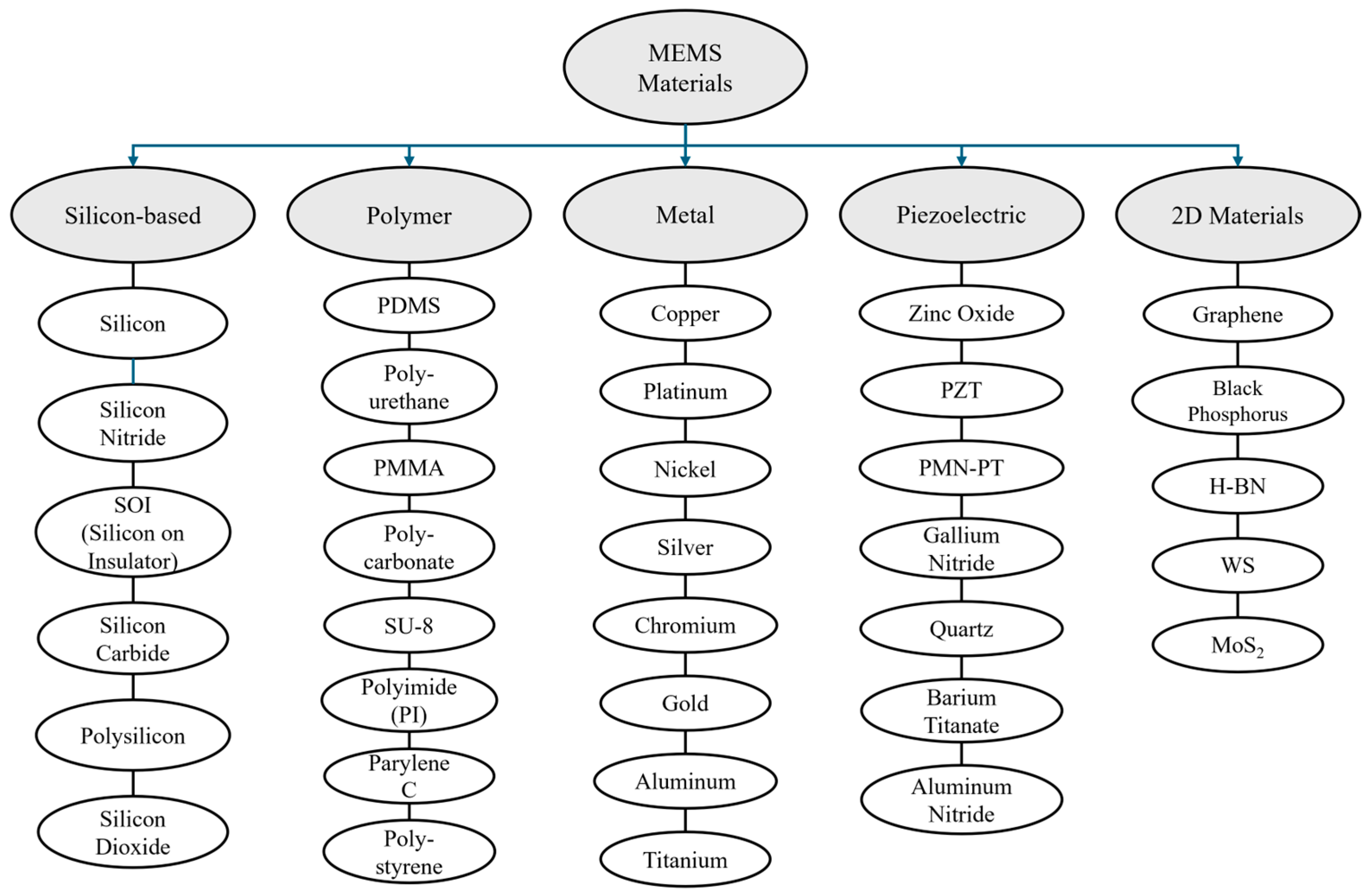
2.1. Materials Used in MEMS Devices
2.1.1. Silicon
2.1.2. Polymers
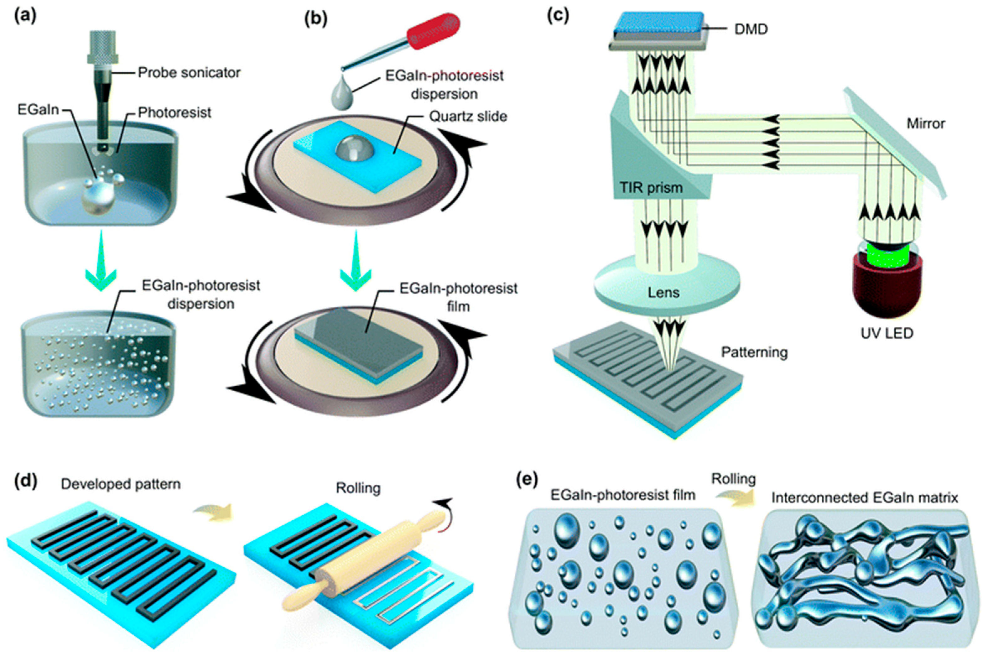
2.1.3. Metals
2.1.4. Piezoelectric
2.1.5. Two-Dimensional Materials
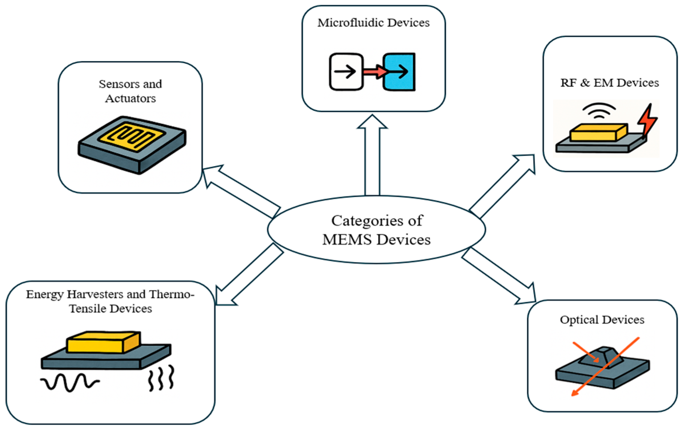
2.2. Categories of MEMS Devices
2.2.1. Sensors and Actuators
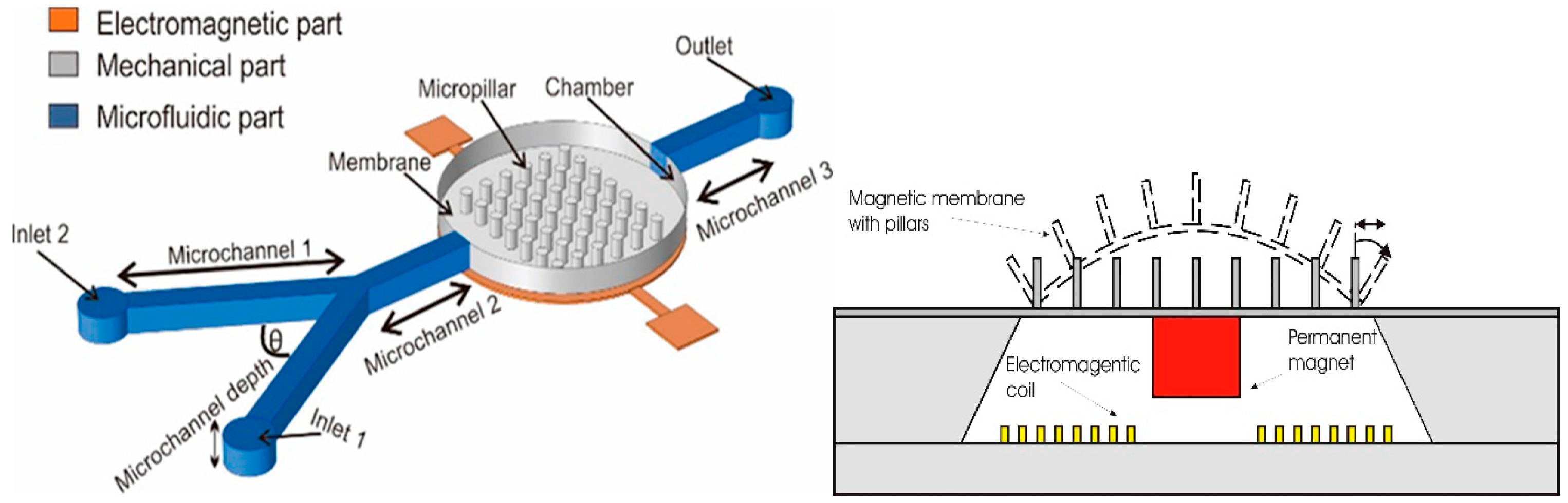
2.2.2. Microfluidic Devices
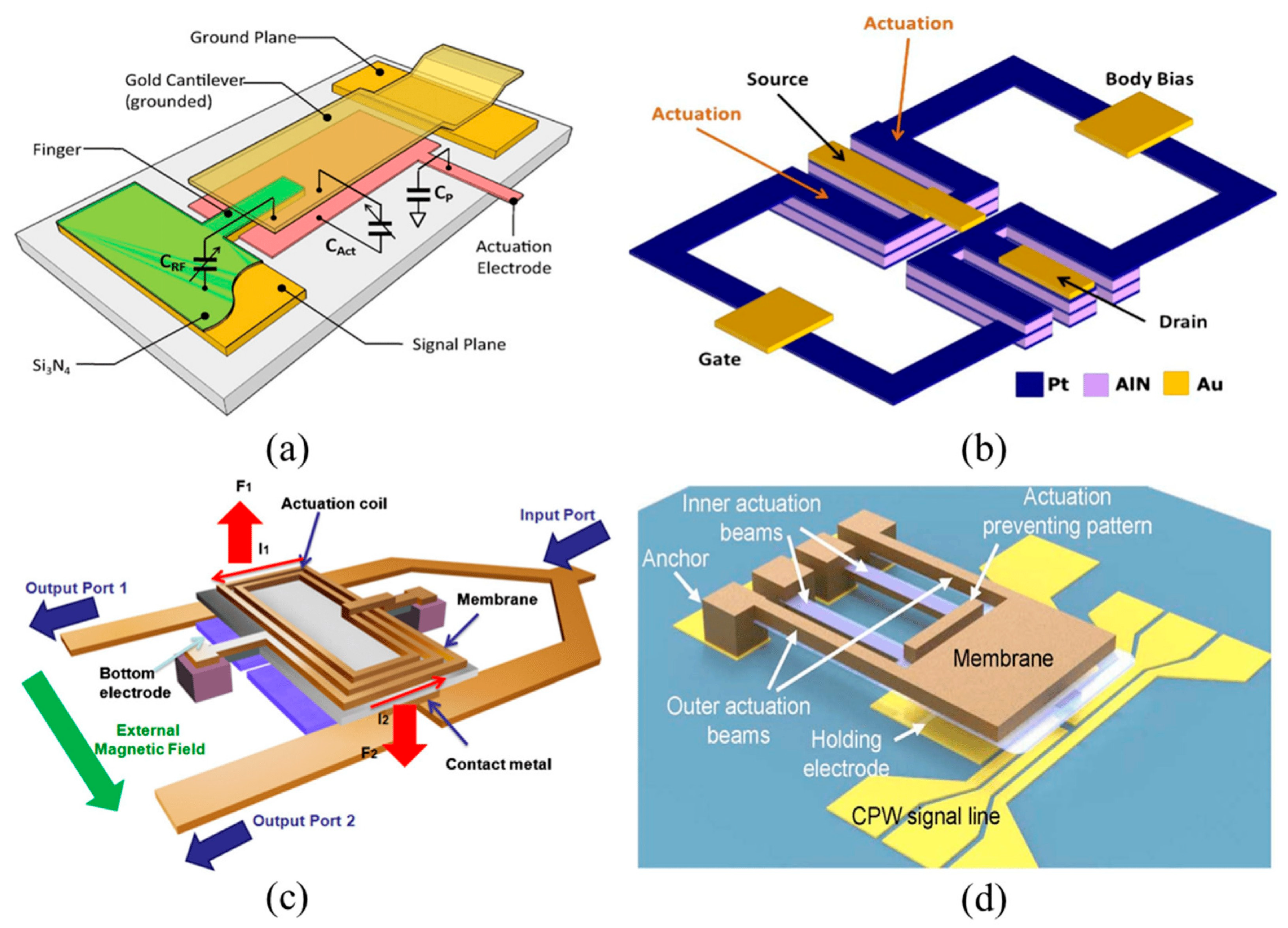
2.2.3. RF and Electromagnetic Devices
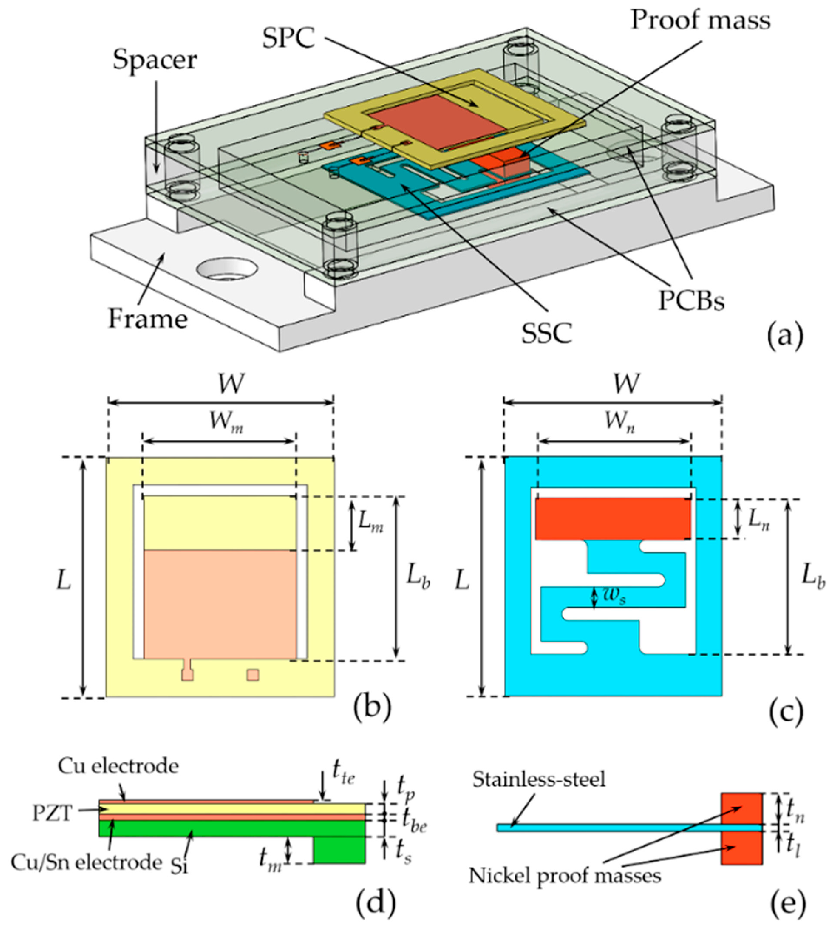
2.2.4. Energy Harvesters and Thermo-Tensile Devices
2.2.5. Optical Devices
3. Manufacturing Processes
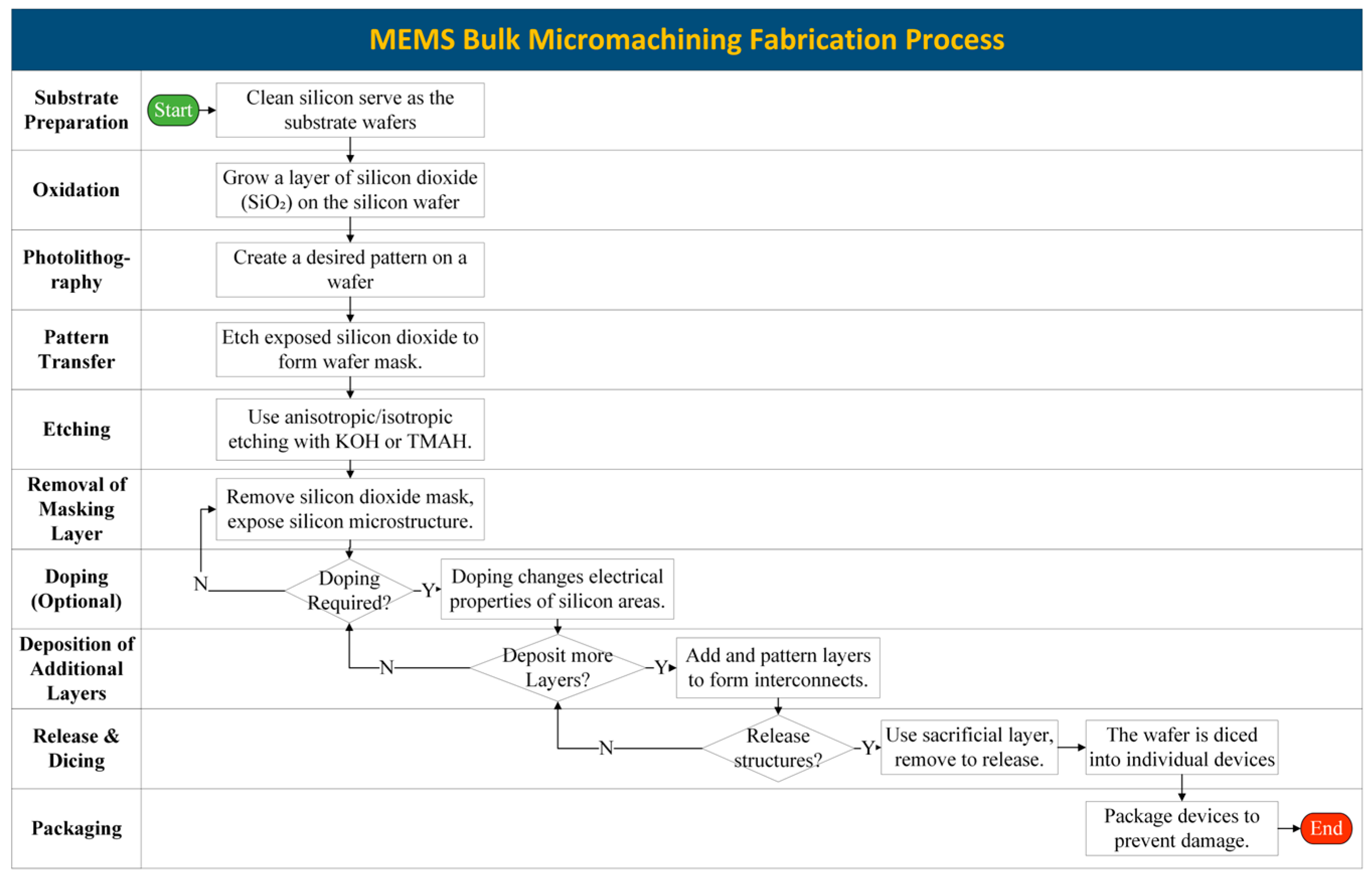
3.1. Bulk Micromachining
3.1.1. Substrate Preparation
3.1.2. Photolithography
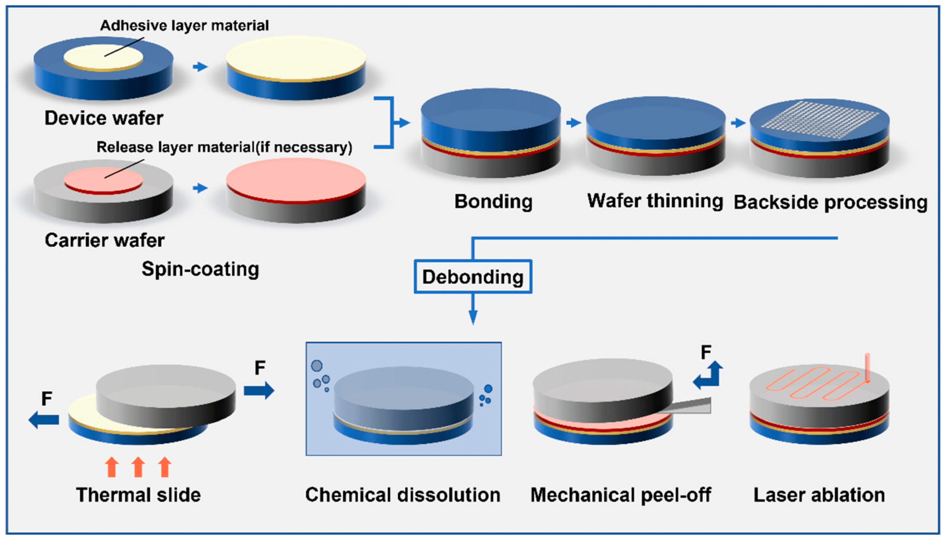
3.1.3. Wafer Bonding
3.1.4. Etching
3.1.5. Release, Assembly, and Packaging
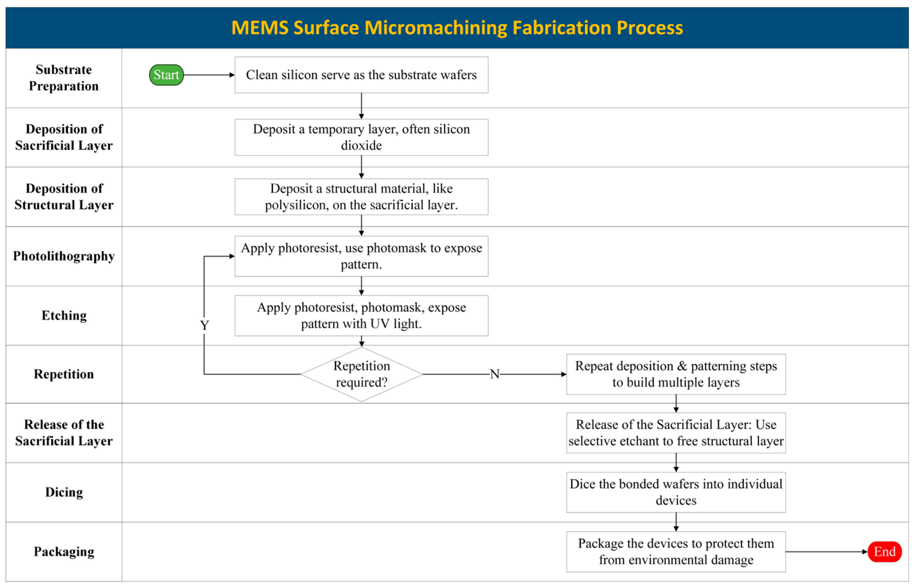
3.2. Surface Micromachining
3.3. LIGA
4. Biomedical Applications
4.1. Biosensors
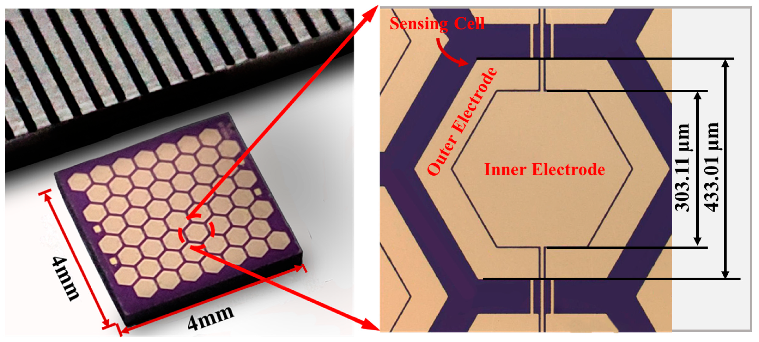
4.1.1. Pressure Sensors
4.1.2. Novel Applications
4.2. Wearable Devices
4.3. Transducers
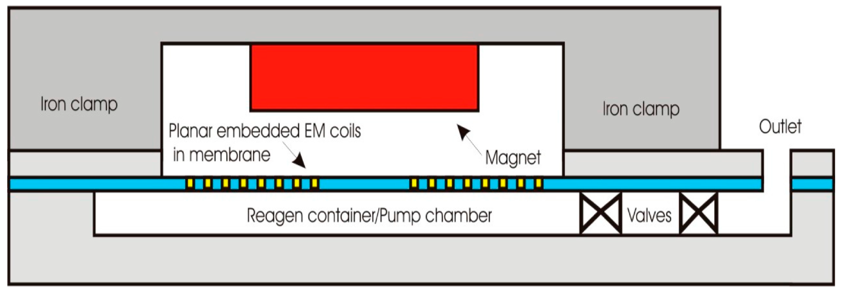
4.4. Microvalves
4.5. Actuators and Circuits
5. Challenges and Prospective Trends
5.1. Current Challenges and Potential Solutions
5.1.1. Biocompatibility, Safety, and Durability
5.1.2. Energy Management
5.1.3. Manufacturing and Scalability
5.1.4. Additive Manufacturing
5.1.5. Standardization
5.2. Prospective Research Trends
5.2.1. AI Integrated Personalized Healthcare
5.2.2. In Situ Energy Harvesting and Robotics
5.2.3. Lab-on-a-Chip
6. Conclusions
Author Contributions
Funding
Institutional Review Board Statement
Informed Consent Statement
Data Availability Statement
Acknowledgments
Conflicts of Interest
References
- Łukasiak, L.; Jakubowski, A. History of Semiconductors. J. Telecommun. Inf. Technol. 2010, 1, 3–9. [Google Scholar] [CrossRef]
- Tai, Y.-C. Introduction to MEMS. In Microsystems and Nanotechnology; Zhou, Z., Wang, Z., Lin, L., Eds.; Springer: Berlin/Heidelberg, Germany, 2012; pp. 187–206. ISBN 978-3-642-18292-1. [Google Scholar]
- Hossain, N.; Mahmud, M.Z.A.; Hossain, A.; Rahman, M.K.; Islam, M.S.; Tasnim, R.; Mobarak, M.H. Advances of Materials Science in MEMS Applications: A Review. Results Eng. 2024, 22, 102115. [Google Scholar] [CrossRef]
- Mohd Ghazali, F.A.; Hasan, M.N.; Rehman, T.; Nafea, M.; Mohamed Ali, M.S.; Takahata, K. MEMS Actuators for Biomedical Applications: A Review. J. Micromech. Microengineering 2020, 30, 073001. [Google Scholar] [CrossRef]
- Ke, C.; Pugno, N.; Peng, B.; Espinosa, H. Experiments and Modeling of Carbon Nanotube-Based NEMS Devices. J. Mech. Phys. Solids 2005, 53, 1314–1333. [Google Scholar] [CrossRef]
- Bhushan, B. Nanotribology and Nanomechanics of MEMS/NEMS and BioMEMS/BioNEMS Materials and Devices. Microelectron. Eng. 2007, 84, 387–412. [Google Scholar] [CrossRef]
- Bhushan, B. Micro/Nanotribology of MEMS/NEMS Materials and Devices. In Springer Handbook of Nanotechnology; Bhushan, B., Ed.; Springer: Berlin/Heidelberg, Germany, 2004; pp. 983–1021. ISBN 978-3-540-01218-4. [Google Scholar]
- Bhushan, B. (Ed.) Fundamentals of Tribology and Bridging the Gap Between the Macro- and Micro/Nanoscales; Springer: Dordrecht, The Netherlands, 2001; ISBN 978-0-7923-6837-3. [Google Scholar]
- Knüttel, T. Laser Texturing of Surfaces in Thin-Film Silicon Photovoltaics-A Comparison of Potential Processes. J. Laser Micro Nanoeng. 2013, 8, 222–229. [Google Scholar] [CrossRef]
- Zorman, C.A.; Parro, R.J. Micro- and Nanomechanical Structures for Silicon Carbide MEMS and NEMS. In Silicon Carbide; Friedrichs, P., Kimoto, T., Ley, L., Pensl, G., Eds.; Wiley: Hoboken, NJ, USA, 2009; pp. 411–451. ISBN 978-3-527-40953-2. [Google Scholar]
- Mehregany, M.; Zorman, C.A.; Rajan, N. Chien Hung Wu Silicon Carbide MEMS for Harsh Environments. Proc. IEEE 1998, 86, 1594–1609. [Google Scholar] [CrossRef]
- Handbook of Silicon Based MEMS Materials and Technologies, 3rd ed.Micro & Nano Technologies Series; Elsevier: Amsterdam, The Netherlands, 2020; ISBN 978-0-12-817786-0.
- Kim, B.J.; Meng, E. Review of Polymer MEMS Micromachining. J. Micromech. Microengineering 2016, 26, 013001. [Google Scholar] [CrossRef]
- Khosla, A.; Gray, B.L. (Invited) Micropatternable Multifunctional Nanocomposite Polymers for Flexible Soft NEMS and MEMS Applications. ECS Trans. 2012, 45, 477–494. [Google Scholar] [CrossRef]
- Yunas, J.; Mulyanti, B.; Hamidah, I.; Mohd Said, M.; Pawinanto, R.E.; Wan Ali, W.A.F.; Subandi, A.; Hamzah, A.A.; Latif, R.; Yeop Majlis, B. Polymer-Based MEMS Electromagnetic Actuator for Biomedical Application: A Review. Polymers 2020, 12, 1184. [Google Scholar] [CrossRef]
- Tambe, N.S.; Bhushan, B. Micro/Nanotribological Characterization of PDMS and PMMA Used for BioMEMS/NEMS Applications. Ultramicroscopy 2005, 105, 238–247. [Google Scholar] [CrossRef]
- Liu, C. Recent Developments in Polymer MEMS. Adv. Mater. 2007, 19, 3783–3790. [Google Scholar] [CrossRef]
- Alonzo, S.M.M.; Bentley, J.; Desai, S.; Bastakoti, B.P. Hydrothermal Synthesis of Hierarchical Microstructure Tungsten Oxide/Carbon Nanocomposite for Supercapacitor Application. Sci. Rep. 2023, 13, 21732. [Google Scholar] [CrossRef] [PubMed]
- Banerjee, A.; Pandey, S.S.; Mastrangelo, C.H. MEMS Stiction Supression with Sacrificial Polystyrene Nanoparticles. In Proceedings of the 2017 IEEE SENSORS, Glasgow, UK, 29 October–1 November 2017; IEEE: Piscataway, NJ, USA; pp. 1–3. [Google Scholar]
- Roussel, M.; Malhaire, C.; Deman, A.-L.; Chateaux, J.-F.; Petit, L.; Seveyrat, L.; Galineau, J.; Guiffard, B.; Seguineau, C.; Desmarres, J.-M.; et al. Electromechanical Study of Polyurethane Films with Carbon Black Nanoparticles for MEMS Actuators. J. Micromech. Microengineering 2014, 24, 055011. [Google Scholar] [CrossRef]
- Reed, H.A.; White, C.E.; Rao, V.; Allen, S.A.B.; Henderson, C.L.; Kohl, P.A. Fabrication of Microchannels Using Polycarbonates as Sacrificial Materials. J. Micromech. Microengineer. 2001, 11, 733–737. [Google Scholar] [CrossRef]
- Hangarter, C.M.; George, T.; Myung, N.V. Electrochemically Fabricated Microelectromechanical Systems/Nanoelectromechanical Systems (MEMS/NEMS). In Electrochemical Nanotechnologies; Osaka, T., Datta, M., Shacham-Diamand, Y., Eds.; Nanostructure Science and Technology; Springer: New York, NY, USA, 2010; pp. 187–226. ISBN 978-1-4419-1423-1. [Google Scholar]
- Panda, A. Electrodeposition of Nickel-Copper Alloys and Nickel-Copper-Alumina Nanocomposites into Deep Recesses for MEMS. Ph.D. Thesis, Louisiana State University and Agricultural and Mechanical College, Baton Rouge, LA, USA, 2003. [Google Scholar]
- Phatthanakun, R.; Deekla, P.; Pummara, W.; Sriphung, C.; Pantong, C.; Chomnawang, N. Fabrication and Control of Thin-Film Aluminum Microheater and Nickel Temperature Sensor. In Proceedings of the 8th Electrical Engineering/Electronics, Computer, Telecommunications and Information Technology (ECTI) Association of Thailand-Conference 2011, Khon Kaen, Thailand, 17–19 May 2011; IEEE: Piscataway, NJ, USA; pp. 14–17. [Google Scholar]
- Hu, T.; Fang, K.; Zhang, Z.; Jiang, X.; Zhao, Y. The Hybrid Fabrication Process of Metal/Silicon Composite Structure for MEMS S&A Device. Micromachines 2019, 10, 469. [Google Scholar] [CrossRef]
- Muralt, P. Recent Progress in Materials Issues for Piezoelectric MEMS. J. Am. Ceram. Soc. 2008, 91, 1385–1396. [Google Scholar] [CrossRef]
- Desai, S.; Lovell, M. Modeling Fluid–Structure Interaction in a Direct Write Manufacturing Process. J. Mater. Process. Technol. 2012, 212, 2031–2040. [Google Scholar] [CrossRef]
- Desai, S.; Lovell, M.; Cordle, J. Coupled Field Analysis of a Piezoelectric Bimorph Disc in a Direct Write Process. Compos. Part B Eng. 2007, 38, 824–832. [Google Scholar] [CrossRef]
- Desai, S.; Lovell, M. Computational Fluid Dynamics Analysis of a Direct Write Manufacturing Process. Int. J. Nanomanuf. 2009, 3, 171–188. [Google Scholar] [CrossRef]
- Wasa, K.; Matsushima, T.; Adachi, H.; Kanno, I.; Kotera, H. Thin-Film Piezoelectric Materials For a Better Energy Harvesting MEMS. J. Microelectromech. Syst. 2012, 21, 451–457. [Google Scholar] [CrossRef]
- Eom, C.-B.; Trolier-McKinstry, S. Thin-Film Piezoelectric MEMS. MRS Bull. 2012, 37, 1007–1017. [Google Scholar] [CrossRef]
- Torkashvand, Z.; Shayeganfar, F.; Ramazani, A. Nanomaterials Based Micro/Nanoelectromechanical System (MEMS and NEMS) Devices. Micromachines 2024, 15, 175. [Google Scholar] [CrossRef] [PubMed]
- Li, X.; Sun, M.; Shan, C.; Chen, Q.; Wei, X. Mechanical Properties of 2D Materials Studied by In Situ Microscopy Techniques. Adv. Mater. Interfaces 2018, 5, 1701246. [Google Scholar] [CrossRef]
- Ferrari, P.F.; Kim, S.; Van Der Zande, A.M. Nanoelectromechanical Systems from Two-Dimensional Materials. Appl. Phys. Rev. 2023, 10, 031302. [Google Scholar] [CrossRef]
- Geim, A.K. Graphene: Status and Prospects. Science 2009, 324, 1530–1534. [Google Scholar] [CrossRef]
- Fan, X.; He, C.; Ding, J.; Gao, Q.; Ma, H.; Lemme, M.C.; Zhang, W. Graphene MEMS and NEMS 2024. Microsyst. Nanoeng. 2024, 10, 154. [Google Scholar] [CrossRef]
- Kommanaboina, N.M. Development of MEMS-Based Devices for Characterizing 2D Nanomaterials at Low Temperatures. Ph.D. Thesis, University of Trento, Trente, Italy, 2023. [Google Scholar]
- Liu, X.; Mwangi, M.; Li, X.; O’Brien, M.; Whitesides, G.M. Paper-Based Piezoresistive MEMS Sensors. Lab. Chip 2011, 11, 2189. [Google Scholar] [CrossRef]
- Eddy, D.S.; Sparks, D.R. Application of MEMS Technology in Automotive Sensors and Actuators. Proc. IEEE 1998, 86, 1747–1755. [Google Scholar] [CrossRef]
- Zhu, J.; Liu, X.; Shi, Q.; He, T.; Sun, Z.; Guo, X.; Liu, W.; Sulaiman, O.B.; Dong, B.; Lee, C. Development Trends and Perspectives of Future Sensors and MEMS/NEMS. Micromachines 2019, 11, 7. [Google Scholar] [CrossRef]
- Du, H.; Chau, F.; Zhou, G. Mechanically-Tunable Photonic Devices with On-Chip Integrated MEMS/NEMS Actuators. Micromachines 2016, 7, 69. [Google Scholar] [CrossRef] [PubMed]
- Ouakad, H.M. Comprehensive Numerical Modeling of the Nonlinear Structural Behavior of MEMS/NEMS Electrostatic Actuators under the Effect of the van Der Waals Forces. Microsyst. Technol. 2017, 23, 5903–5910. [Google Scholar] [CrossRef]
- Meng, F.; Zhang, C.; Zhang, G.; Renxin, W.; He, C.; Yang, Y.; Cui, J.; Zhang, W.; Jia, L. A Novel AlN/Sc0. 2Al0.8N-Based Piezoelectric Composite Thin-Film-Enabled Bioinspired Honeycomb MEMS Hydrophone 2025, 16, 454. [Google Scholar] [CrossRef]
- Islam, N. (Ed.) Microelectromechanical Systems and Devices; InTech: London, UK, 2012; ISBN 978-953-51-0306-6. [Google Scholar]
- Vyawahare, S.; Griffiths, A.D.; Merten, C.A. Miniaturization and Parallelization of Biological and Chemical Assays in Microfluidic Devices. Chem. Biol. 2010, 17, 1052–1065. [Google Scholar] [CrossRef]
- Desai, S.; Perkins, J.; Harrison, B.S.; Sankar, J. Understanding Release Kinetics of Biopolymer Drug Delivery Microcapsules for Biomedical Applications. Mater. Sci. Eng. B 2010, 168, 127–131. [Google Scholar] [CrossRef]
- Aldawood, F.K.; Parupelli, S.K.; Andar, A.; Desai, S. 3D Printing of Biodegradable Polymeric Microneedles for Transdermal Drug Delivery Applications. Pharmaceutics 2024, 16, 237. [Google Scholar] [CrossRef]
- Perkins, J.; Yi, H.; Ye, S.H.; Wagner, W.; Desai, S. Direct Write Manufacturing of Controlled Release Coatings for Drug Eluting Cardiovascular Stents. J. Bio. Med. Res. Part A 2014, 102, 4290–4300. [Google Scholar]
- Adarkwa, E.; Roy, A.; Ohodnicki, J.; Lee, B.; Kumta, P.N.; Desai, S. 3D Printing of Drug-Eluting Bioactive Multifunctional Coatings for Orthopedic Applications. Int. J. Bioprinting 2023, 9, 661. [Google Scholar] [CrossRef]
- Lin, L.; Chung, C.-K. PDMS Microfabrication and Design for Microfluidics and Sustainable Energy Application: Review. Micromachines 2021, 12, 1350. [Google Scholar] [CrossRef]
- Madou, M.J. Fundamentals of Microfabrication: The Science of Miniaturization; CRC Press: Boca Raton, FL, USA, 2018. [Google Scholar]
- Hilbert, J.L. RF-MEMS for Wireless Communications. IEEE Commun. Mag. 2008, 46, 68–74. [Google Scholar] [CrossRef]
- Shao, B.; Lu, C.; Xiang, Y.; Li, F.; Song, M. Comprehensive Review of RF MEMS Switches in Satellite Communications. Sensors 2024, 24, 3135. [Google Scholar] [CrossRef] [PubMed]
- Will-Cole, A.R.; Hassanien, A.E.; Calisgan, S.D.; Jeong, M.-G.; Liang, X.; Kang, S.; Rajaram, V.; Martos-Repath, I.; Chen, H.; Risso, A.; et al. Tutorial: Piezoelectric and Magnetoelectric N/MEMS—Materials, Devices, and Applications. J. Appl. Phys. 2022, 131, 241101. [Google Scholar] [CrossRef]
- Luo, B.; Will-Cole, A.R.; Dong, C.; He, Y.; Liu, X.; Lin, H.; Huang, R.; Shi, X.; McConney, M.; Page, M.; et al. Magnetoelectric Microelectromechanical and Nanoelectromechanical Systems for the IoT. Nat. Rev. Electr. Eng. 2024, 1, 317–334. [Google Scholar] [CrossRef]
- Safaei, M.; Sodano, H.A.; Anton, S.R. A Review of Energy Harvesting Using Piezoelectric Materials: State-of-the-Art a Decade Later (2008–2018). Smart Mater. Struct. 2019, 28, 113001. [Google Scholar] [CrossRef]
- Gu, L. Low-Frequency Piezoelectric Energy Harvesting Prototype Suitable for the MEMS Implementation. Microelectron. J. 2011, 42, 277–282. [Google Scholar] [CrossRef]
- Huang, M.; Hou, C.; Li, Y.; Liu, H.; Wang, F.; Chen, T.; Yang, Z.; Tang, G.; Sun, L. A Low-Frequency MEMS Piezoelectric Energy Harvesting System Based on Frequency Up-Conversion Mechanism. Micromachines 2019, 10, 639. [Google Scholar] [CrossRef]
- Springer Handbook of Nanotechnology, 3rd ed.; Bhushan, B., Ed.; Springer: Berlin, Germany; New York, NY, USA, 2010; ISBN 978-3-642-02524-2. [Google Scholar]
- Solgaard, O.; Godil, A.A.; Howe, R.T.; Lee, L.P.; Peter, Y.-A.; Zappe, H. Optical MEMS: From Micromirrors to Complex Systems. J. Microelectromech. Syst. 2014, 23, 517–538. [Google Scholar] [CrossRef]
- Tsai, C.; Tsai, J. MEMS Optical Switches and Interconnects. Displays 2015, 37, 33–40. [Google Scholar] [CrossRef]
- Wu, M.C.; Solgaard, O.; Ford, J.E. Optical MEMS for Lightwave Communication. J. Light Technol. 2006, 24, 4433–4454. [Google Scholar] [CrossRef]
- Ma, X.; Kuo, G.-S. Optical Switching Technology Comparison: Optical Mems vs. Other Technologies. IEEE Commun. Mag. 2003, 41, 50–57. [Google Scholar] [CrossRef]
- Misrak, A.; Chauhan, T.; Bhandari, R.; Chowdhury, A.R.; Lakshminarayana, A.; Mirza, F.; Bazehhour, B.G.; Vujosevic, M.; Agonafer, D. Impact of Die Attach Sample Preparation on Its Measured Mechanical Properties for MEMS Sensor Applications. J. Microelectron. Electron. Packag. 2021, 18, 21–28. [Google Scholar] [CrossRef]
- Mohammed, A.A.; Moussa, W.A.; Lou, E. High Sensitivity MEMS Strain Sensor: Design and Simulation. Sensors 2008, 8, 2642–2661. [Google Scholar] [CrossRef] [PubMed]
- Blachowicz, T.; Ehrmann, A. 3D Printed MEMS Technology—Recent Developments and Applications. Micromachines 2020, 11, 434. [Google Scholar] [CrossRef] [PubMed]
- Abbasi, R.; Mayyas, M.; Ghasemian, M.B.; Centurion, F.; Yang, J.; Saborio, M.; Allioux, F.-M.; Han, J.; Tang, J.; Christoe, M.J.; et al. Photolithography–Enabled Direct Patterning of Liquid Metals. J. Mater. Chem. C 2020, 8, 7805–7811. [Google Scholar] [CrossRef]
- Barajas-Valdes, U.; Suárez, O.M. Nanomechanical Properties of Thin Films Manufactured via Magnetron Sputtering from Pure Aluminum and Aluminum-Boron Targets. Thin Solid Film. 2020, 693, 137670. [Google Scholar] [CrossRef]
- Davranche, M.; Bollinger, J.-C. Release of Metals from Iron Oxyhydroxides under Reductive Conditions: Effect of Metal/Solid Interactions. J. Colloid Interface Sci. 2000, 232, 165–173. [Google Scholar] [CrossRef]
- Salehi, M.; Heidari, P.; Ruhani, B.; Kheradmand, A.; Purcar, V.; Căprărescu, S. Theoretical and Experimental Analysis of Surface Roughness and Adhesion Forces of MEMS Surfaces Using a Novel Method for Making a Compound Sputtering Target. Coatings 2021, 11, 1551. [Google Scholar] [CrossRef]
- Mo, Z.; Wang, F.; Li, J.; Liu, Q.; Zhang, G.; Li, W.; Yang, C.; Sun, R. Temporary Bonding and Debonding in Advanced Packaging: Recent Progress and Applications. Electronics 2023, 12, 1666. [Google Scholar] [CrossRef]
- Pal, P.; Sato, K.; Gosalvez, M.A.; Shikida, M. Study of Rounded Concave and Sharp Edge Convex Corners Undercutting in CMOS Compatible Anisotropic Etchants. J. Micromech. Microengineer. 2007, 17, 2299–2307. [Google Scholar] [CrossRef]
- Pal, P.; Sato, K. Fabrication Methods Based on Wet Etching Process for the Realization of Silicon MEMS Structures with New Shapes. Microsyst. Technol. 2010, 16, 1165–1174. [Google Scholar] [CrossRef]
- De Boer, M.J.; Gardeniers, J.G.E.; Jansen, H.V.; Smulders, E.; Gilde, M.-J.; Roelofs, G.; Sasserath, J.N.; Elwenspoek, M. Guidelines for Etching Silicon MEMS Structures Using Fluorine High-Density Plasmas at Cryogenic Temperatures. J. Microelectromechanical Syst. 2002, 11, 385–401. [Google Scholar] [CrossRef]
- Li, H.; Ruan, Y.; You, Z.; Song, Z. Design and Fabrication of a Novel MEMS Relay with Low Actuation Voltage. Micromachines 2020, 11, 171. [Google Scholar] [CrossRef] [PubMed]
- Cao, T.; Hu, T.; Zhao, Y. Research Status and Development Trend of MEMS Switches: A Review. Micromachines 2020, 11, 694. [Google Scholar] [CrossRef] [PubMed]
- Fogel, O.; Winter, S.; Benjamin, E.; Krylov, S.; Kotler, Z.; Zalevsky, Z. 3D printing of functional metallic microstructures and its implementation in electrothermal actuators. Addit. Manuf. 2018, 21, 307–311. [Google Scholar] [CrossRef]
- Zhang, Y.-F.; Cui, M.; Wu, D.-P. Design and Fabrication of a MEMS Bandpass Filter with Different Center Frequency of 8.5–12 GHz. Micromachines 2023, 14, 280. [Google Scholar] [CrossRef]
- Lee, S.; Park, S.; Cho, D.-I. The Surface/Bulk Micromachining (SBM) Process: A New Method for Fabricating Released MEMS in Single Crystal Silicon. J. Microelectromechanical Syst. 1999, 8, 409–416. [Google Scholar]
- Kauzlarick, D. Fundamentals of Microfabrication, the Science of Miniaturization, 2nd Edition [Book Review]. IEEE Eng. Med. Biol. Mag. 2003, 22, 109–111. [Google Scholar] [CrossRef]
- Nguyen, N.-T.; Hejazian, M.; Ooi, C.; Kashaninejad, N. Recent Advances and Future Perspectives on Microfluidic Liquid Handling. Micromachines 2017, 8, 186. [Google Scholar] [CrossRef]
- Bio-MEMS: Technologies and Applications, 1st ed.; Wang, W., Soper, S.A., Eds.; CRC Press: Boca Raton, FL, USA, 2006; ISBN 978-0-429-11405-2. [Google Scholar]
- Parupelli, S.K.; Desai, S. The 3D Printing of Nanocomposites for Wearable Biosensors: Recent Advances, Challenges, and Prospects. Bioengineering 2023, 11, 32. [Google Scholar] [CrossRef]
- Desai, S.; Bidanda, B.; Bártolo, P.J. Emerging Trends in the Applications of Metallic and Ceramic Biomaterials. In Bio-Materials and Prototyping Applications in Medicine; Springer: Cham, Switzerland, 2021; pp. 1–17. [Google Scholar]
- Desai, S.; Shankar, M.R. Emerging Trends in Polymers, Composites, and Nano Biomaterial Applications. In Bio-Materials and Prototyping Applications in Medicine; Springer: Cham, Switzerland, 2021; pp. 19–24. [Google Scholar]
- Hajare, R.; Reddy, V.; Srikanth, R. MEMS Based Sensors–A Comprehensive Review of Commonly Used Fabrication Techniques. Mater. Today Proc. 2022, 49, 720–730. [Google Scholar] [CrossRef]
- Nazir, S.; Kwon, O.S. Micro-Electromechanical Systems-Based Sensors and Their Applications. Appl. Sci. Converg. Technol. 2022, 31, 40–45. [Google Scholar] [CrossRef]
- Varney, M.W.; Aslam, D.M.; Janoudi, A.; Chan, H.-Y.; Wang, D.H. Polycrystalline-Diamond MEMS Biosensors Including Neural Microelectrode-Arrays. Biosensors 2011, 1, 118–133. [Google Scholar] [CrossRef] [PubMed]
- Yunus, N.A.M.; Halin, I.A.; Sulaiman, N.; Ismail, N.F.; Sheng, O.K. Valuation on MEMS Pressure Sensors and Device Applications. Int. J. Electron. Commun. Eng. 2015, 9, 834–842. [Google Scholar]
- Lakshmai, G.S.; Rao, K.S.; Sravani, K.G. Design and Analysis of MEMS Pressure Sensor Based on Various Principles of Microcantilever Beam. IEEE Trans. NanoBiosci. 2023, 24, 2–15. [Google Scholar] [CrossRef]
- Kolluri, S.S.K.; Durai, S.A. Wearable Micro-electro-mechanical Systems Pressure Sensors in Health Care: Advancements and Trends—A Review. IET Wirel. Sens. Syst. 2024, 14, 233–247. [Google Scholar] [CrossRef]
- Rohan, R.; Venkadeshwaran, K. Measurement of Human Blood Pressure Using Mems Pressure Sensor. In Proceedings of the 2022 9th International Conference on Computing for Sustainable Global Development (INDIACom), New Delhi, India, 23–25 March 2022; IEEE: Piscataway, NJ, USA; pp. 99–103. [Google Scholar]
- Chattopadhyay, M.; Chowdhury, D. Design and Performance Analysis of MEMS Capacitive Pressure Sensor Array for Measurement of Heart Rate. Microsyst. Technol. 2017, 23, 4203–4209. [Google Scholar] [CrossRef]
- Kalvesten, E.; Smith, L.; Tenerz, L.; Stemme, G. The First Surface Micromachined Pressure Sensor for Cardiovascular Pressure Measurements. In Proceedings of the Proceedings MEMS 98. IEEE. Eleventh Annual International Workshop on Micro Electro Mechanical Systems. An Investigation of Micro Structures, Sensors, Actuators, Machines and Systems (Cat. No. 98CH36176), Heidelberg, Germany, 25–29 January 1998; IEEE: Piscataway, NJ, USA; pp. 574–579. [Google Scholar]
- Meena, K.V.; Sankar, A.R. Biomedical Catheters with Integrated Miniature Piezoresistive Pressure Sensors: A Review. IEEE Sens. J. 2021, 21, 10241–10290. [Google Scholar] [CrossRef]
- Pandey, Y.; Singh, S.P. Recent Advances in Bio-MEMS and Future Possibilities: An Overview. J. Inst. Eng. India Ser. B 2023, 104, 1377–1388. [Google Scholar] [CrossRef]
- Abdul, B. Development of a Novel Silicon Membrane MEMS Capacitive Pressure Sensor for Biological Applications. Eng. Proc. 2023, 48, 54. [Google Scholar]
- Chircov, C.; Grumezescu, A.M. Microelectromechanical Systems (MEMS) for Biomedical Applications. Micromachines 2022, 13, 164. [Google Scholar] [CrossRef]
- Vante, A.B.; Kanish, T.C. Fluid-Structure Interaction and Experimental Studies of Passive Check Valve Based Piezoelectric Micropump for Biomedical Applications. Adv. Mater. Process. Technol. 2024, 10, 2095–2121. [Google Scholar] [CrossRef]
- He, J.-H.; He, C.-H.; Qian, M.-Y.; Alsolami, A.A. Piezoelectric Biosensor Based on Ultrasensitive MEMS System. Sens. Actuators Phys. 2024, 376, 115664. [Google Scholar] [CrossRef]
- Wu, N.; Tian, Y.; Zou, X.; Zhai, Y.; Barringhaus, K.; Wang, X. A Miniature Fiber Optic Blood Pressure Sensor and Its Application in in Vivo Blood Pressure Measurements of a Swine Model. Sens. Actuators B Chem. 2013, 181, 172–178. [Google Scholar] [CrossRef]
- Young, D.J. Interface Electronics for MEMS-Based Wireless Sensing Applications. In Proceedings of the 2010 International Symposium on VLSI Design, Automation and Test, Hsinchu, Taiwan, 26–29 April 2010; IEEE: Piscataway, NJ, USA; pp. 130–133. [Google Scholar]
- Kulkarni, M.B.; Ayachit, N.H.; Aminabhavi, T.M. Biosensors and Microfluidic Biosensors: From Fabrication to Application. Biosensors 2022, 12, 543. [Google Scholar] [CrossRef]
- Microengineering Aerospace Systems. Helvajian, H. (Ed.) Aerospace Press: El Segundo, CA, USA; American Institute of Aeronautics and Astronautics: Reston, VA, USA, 1999; ISBN 978-1-884989-03-2. [Google Scholar]
- Belyustin, A.A. The Centenary of Glass Electrode: From Max Cremer to F. G. K. Baucke. J. Solid State Electrochem. 2011, 15, 47–65. [Google Scholar] [CrossRef]
- Clark, L.C.; Wolf, R.; Granger, D.; Taylor, Z. Continuous Recording of Blood Oxygen Tensions by Polarography. J. Appl. Physiol. 1953, 6, 189–193. [Google Scholar] [CrossRef]
- Barlian, A.A.; Park, W.-T.; Mallon, J.R.; Rastegar, A.J.; Pruitt, B.L. Review: Semiconductor Piezoresistance for Microsystems. Proc. IEEE 2009, 97, 513–552. [Google Scholar] [CrossRef]
- Gatzen, H.H.; Saile, V.; Leuthold, J. Introduction—MEMS, a Historical Perspective. In Micro and Nano Fabrication; Springer: Berlin/Heidelberg, Germany, 2015; pp. 1–5. ISBN 978-3-662-44394-1. [Google Scholar]
- Sander, C.S.; Knutti, J.W.; Meindl, J.D. A Monolithic Capacitive Pressure Sensor with Pulse-Period Output. IEEE Trans. Electron Devices 1980, 27, 927–930. [Google Scholar] [CrossRef]
- Michaels, J.E.; Michaels, T.E. Detection of Structural Damage from the Local Temporal Coherence of Diffuse Ultrasonic Signals. IEEE Trans. Ultrason. Ferroelectr. Freq. Control 2005, 52, 1769–1782. [Google Scholar] [CrossRef]
- Kaisti, M.; Panula, T.; Leppänen, J.; Punkkinen, R.; Tadi, M.J.; Vasankari, T.; Jaakkola, S.; Kiviniemi, T.; Airaksinen, J.; Kostiainen, P. Clinical Assessment of a Non-Invasive Wearable MEMS Pressure Sensor Array for Monitoring of Arterial Pulse Waveform, Heart Rate and Detection of Atrial Fibrillation. NPJ Digit. Med. 2019, 2, 39. [Google Scholar] [CrossRef]
- Al-Qatatsheh, A.; Morsi, Y.; Zavabeti, A.; Zolfagharian, A.; Salim, N.; Kouzani, A.Z.; Mosadegh, B.; Gharaie, S. Blood Pressure Sensors: Materials, Fabrication Methods, Performance Evaluations and Future Perspectives. Sensors 2020, 20, 4484. [Google Scholar] [CrossRef] [PubMed]
- Polat, E.O.; Cetin, M.M.; Tabak, A.F.; Güven, E.B.; Uysal, B.Ö.; Arsan, T.; Kabbani, A.; Hamed, H.; Gül, S.B. Transducer Technologies for Biosensors and Their Wearable Applications. Biosensors 2022, 12, 385. [Google Scholar] [CrossRef] [PubMed]
- Eidi, A. Design and Evaluation of an Implantable MEMS Based Biosensor for Blood Analysis and Real-Time Measurement. Microsyst. Technol. 2023, 29, 857–864. [Google Scholar] [CrossRef]
- Lakshmi, G.S.; Karumuri, S.R.; Kondavitee, G.S.; Lay-Ekuakille, A. Design and Performance Analysis of a Microbridge and Microcantilever-Based MEMS Pressure Sensor for Glucose Monitoring. IEEE Sens. J. 2023, 23, 4589–4596. [Google Scholar] [CrossRef]
- Gemelli, A.; Tambussi, M.; Fusetto, S.; Aprile, A.; Moisello, E.; Bonizzoni, E.; Malcovati, P. Recent Trends in Structures and Interfaces of MEMS Transducers for Audio Applications: A Review. Micromachines 2023, 14, 847. [Google Scholar] [CrossRef]
- Hamed, H.; Eldiasty, M.; Seyedi-Sahebari, S.-M.; Abou-Ziki, J.D. Applications, Materials, and Fabrication of Micro Glass Parts and Devices: An Overview. Mater. Today 2023, 66, 194–220. [Google Scholar] [CrossRef]
- Cugno, M. Light Actuated Microvalve. Ph.D. Thesis, Worcester Polytechnic Institute, Worcester, MA, USA, 2022. [Google Scholar]
- Richter, M.; Anheuer, D.; Wille, A.; Congar, Y.; Wackerle, M. Multistage Micropump System towards Vacuum Pressure. Actuators 2023, 12, 227. [Google Scholar] [CrossRef]
- Ficai, D.; Gheorghe, M.; Dolete, G.; Mihailescu, B.; Svasta, P.; Ficai, A.; Constantinescu, G.; Andronescu, E. Microelectromechanical Systems Based on Magnetic Polymer Films. Micromachines 2022, 13, 351. [Google Scholar] [CrossRef]
- Matsubara, T.; Choi, J.S.; Kim, D.-H.; Kim, J. A Microfabricated Pistonless Syringe Pump Driven by Electro-Conjugate Fluid with Leakless On/Off Microvalves. Small 2022, 18, 2106221. [Google Scholar] [CrossRef]
- Li, B.; Zhang, L.; Bai, S.; Jin, J.; Chen, H. A Brief Overview of Passive Microvalves in Microfluidics: Mechanism, Manufacturing, and Applications. Biomicrofluidics 2024, 18, 021506. [Google Scholar] [CrossRef] [PubMed]
- Gavali, S.R.; Pawar, P.M. Computational Analysis of a Four-Flap Valveless Micropump (FFVM) for Low Reynolds Number Applications in Microfluidic Systems. Phys. Scr. 2024, 99, 075011. [Google Scholar] [CrossRef]
- Khadanga, S. Fabrication of MEMS Pressure Sensor on Thin Film Membrane. Engpaper J. 2021, 9, 10–16. [Google Scholar]
- Vyas, S.; Alhussainy, A.K.; Raju, Y.K.; Manjunatha, M.; Srivastava, A.P.; Jain, A.; Vijetha, T. Analytical Review on Enhancing Sustainability in Microsystems by Integrating MEMS for Compact Design. E3S Web Conf. EDP Sci. 2024, 552, 01108. [Google Scholar] [CrossRef]
- Arnoult, T.; Leclercq, C.; Ghouila-Houri, C.; Mazzamurro, A.; Viard, R.; Garnier, E.; Poussot-Vassal, C.; Merlen, A.; Sipp, D.; Pernod, P. Subsonic Cavity Flow Control with Micro-Magneto-Mechanical Systems (MMMS) Microvalves. Sens. Actuators Phys. 2023, 354, 114257. [Google Scholar] [CrossRef]
- Morkvenaite-Vilkonciene, I.; Bucinskas, V.; Subaciute-Zemaitiene, J.; Sutinys, E.; Virzonis, D.; Dzedzickis, A. Development of Electrostatic Microactuators: 5-Year Progress in Modeling, Design, and Applications. Micromachines 2022, 13, 1256. [Google Scholar] [CrossRef]
- Sharma, S.; Kohli, N.; Brière, J.; Nabki, F.; Ménard, M. Integrated 1× 3 MEMS Silicon Nitride Photonics Switch. Opt. Express 2022, 30, 22200–22220. [Google Scholar] [CrossRef]
- Aishan, Y.; Funano, S.; Sato, A.; Ito, Y.; Ota, N.; Yalikun, Y.; Tanaka, Y. Bio-Actuated Microvalve in Microfluidics Using Sensing and Actuating Function of Mimosa Pudica. Sci. Rep. 2022, 12, 7653. [Google Scholar] [CrossRef]
- Huang, X.; Li, S.; Schultz, J.S.; Wang, Q.; Lin, Q. A MEMS Affinity Glucose Sensor Using a Biocompatible Glucose-Responsive Polymer. Sens. Actuators B Chem. 2009, 140, 603–609. [Google Scholar] [CrossRef]
- Ni, M.; Tong, W.H.; Choudhury, D.; Rahim, N.A.A.; Iliescu, C.; Yu, H. Cell Culture on MEMS Platforms: A Review. Int. J. Mol. Sci. 2009, 10, 5411–5441. [Google Scholar] [CrossRef]
- Christensen, T.B.; Pedersen, C.M.; Gröndahl, K.G.; Jensen, T.G.; Sekulovic, A.; Bang, D.D.; Wolff, A. PCR Biocompatibility of Lab-on-a-Chip and MEMS Materials. J. Micromech. Microengineering 2007, 17, 1527–1532. [Google Scholar] [CrossRef]
- Voskerician, G.; Shive, M.S.; Shawgo, R.S.; Recum, H.V.; Anderson, J.M.; Cima, M.J.; Langer, R. Biocompatibility and Biofouling of MEMS Drug Delivery Devices. Biomaterials 2003, 24, 1959–1967. [Google Scholar] [CrossRef] [PubMed]
- Kotzar, G.; Freas, M.; Abel, P.; Fleischman, A.; Roy, S.; Zorman, C.; Moran, J.M.; Melzak, J. Evaluation of MEMS Materials of Construction for Implantable Medical Devices. Biomaterials 2002, 23, 2737–2750. [Google Scholar] [CrossRef] [PubMed]
- Hopcroft, M.A.; Nix, W.D.; Kenny, T.W. What Is the Young’s Modulus of Silicon? J. Microelectromechanical Syst. 2010, 19, 229–238. [Google Scholar] [CrossRef]
- Villanueva, L.G.; Bausells, J.; Brugger, J. Grand Challenge in N/MEMS. Front. Mech. Eng. 2016, 1, 15. [Google Scholar] [CrossRef]
- Ionov, L. Hydrogel-Based Actuators: Possibilities and Limitations. Mater. Today 2014, 17, 494–503. [Google Scholar] [CrossRef]
- Medical Devices–Angela N Johnson. Available online: https://angelanjohnson.com/medicaldevices/ (accessed on 15 November 2024).
- Alzgool, M.; Tian, Y.; Davaji, B.; Towfighian, S. Self-Powered Triboelectric MEMS Accelerometer. Nano Energy 2023, 109, 108282. [Google Scholar] [CrossRef]
- Mousavi, M.; Alzgool, M.; Davaji, B.; Towfighian, S. Event-Driven MEMS Vibration Sensor: Integration of Triboelectric Nanogenerator and Low-Frequency Switch. Mech. Syst. Signal Process. 2023, 187, 109921. [Google Scholar] [CrossRef]
- National, R.C. Microelectromechanical Systems: Advanced Materials and Fabrication Methods; The National Academies Press: Washington, DC, USA, 1997; ISBN 978-0-309-05980-0. [Google Scholar]
- Rao, R. An Introduction to MEMS (Micro-Electromechanical Systems). Prime Faraday Technol. Watch. 2022. Available online: https://www.academia.edu/5077471/Prime_Faraday_Technology_Watch_ISBN_1_84402_020_7_An_Introduction_to_MEMS_An_Introduction_to_MEMS_Micro_electromechanical_Systems_PRIME_Faraday_Partnership_PRIME_Faraday_Partnership (accessed on 20 November 2024).
- Adarkwa, E.; Kotoka, R.; Desai, S. 3D Printing of Polymeric Coatings on AZ31 Mg Alloy Substrate for Corrosion Protection of Biomedical Implants. Med. Devices Sens. 2021, 4, e10167. [Google Scholar] [CrossRef]
- Kumar_Parupelli, S.; Saudi, S.; Bhattarai, N.; Desai, S. 3D Printing of PCL-Ceramic Composite Scaffolds for Bone Tissue Engineering Applications. Int. J. Bioprinting 2023, 9, 196. [Google Scholar]
- Parupelli, S.K.; Desai, S. Hybrid Additive Manufacturing (3D Printing) and Characterization of Functionally Gradient Materials via in Situ Laser Curing. Int. J. Adv. Manuf. Technol. 2020, 110, 543–556. [Google Scholar] [CrossRef]
- Ogunsanya, M.; Isichei, J.; Desai, S. Grid Search Hyperparameter Tuning in Additive Manufacturing Processes. Manuf. Lett. 2023, 35, 1031–1042. [Google Scholar] [CrossRef]
- Yang, M.; Parupelli, S.K.; Xu, Z.; Desai, S. Understanding the Effect of Dispersant Rheology and Binder Decomposition on 3D Printing of a Solid Oxide Fuel Cell. Micromachines 2024, 15, 636. [Google Scholar] [CrossRef] [PubMed]
- Yang, M.; Parupelli, S.K.; Xu, Z.; Desai, S. Three-Dimensional-Printed Composite Structures: The Effect of LSCF Slurry Solid Loading, Binder, and Direct-Write Process Parameters. Materials 2024, 17, 2822. [Google Scholar] [CrossRef]
- Marquetti, I.; Desai, S. Molecular Modeling the Adsorption Behavior of Bone Morphogenetic Protein-2 on Hydrophobic and Hydrophilic Substrates. Chem. Phys. Lett. 2018, 706, 285–294. [Google Scholar] [CrossRef]
- Marquetti, I.; Desai, S. Nanoscale Topographical Effects on the Adsorption Behavior of Bone Morphogenetic Protein-2 on Graphite. Int. J. Mol. Sci. 2022, 23, 2432. [Google Scholar] [CrossRef]
- Marquetti, I.; Desai, S. Orientation Effects on the Nanoscale Adsorption Behavior of Bone Morphogenetic Protein-2 on Hydrophilic Silicon Dioxide. RSC Adv. 2019, 9, 906–916. [Google Scholar] [CrossRef]
- Plander, I.; Stepanovsky, M. MEMS Optical Switch: Switching Time Reduction. Open Comput. Sci. 2016, 6, 116–125. [Google Scholar] [CrossRef]
- Kasambe, P.V.; Bhole, K.S.; Raykar, N.R.; Oza, A.D.; Ramesh, R.; Bhoir, D.V. Mechanical Modeling, Numerical Investigation and Design of Cantilever Beam for Low Pull-in MEMS Switch. Int. J. Interact. Des. Manuf. IJIDeM 2022, 1–10. [Google Scholar] [CrossRef]
- Yazdanpanah, Z.; Johnston, J.D.; Cooper, D.M.; Chen, X. 3D Bioprinted Scaffolds for Bone Tissue Engineering: State-of-the-Art and Emerging Technologies. Front. Bioeng. Biotechnol. 2022, 10, 824156. [Google Scholar] [CrossRef]
- Ertugrul, I.; Akkus, N.; Yuce, H. Fabrication of MEMS-based electrothermal microactuators with additive manufacturing technologies. Mater. Tehnol. 2019, 53, 665–670. [Google Scholar] [CrossRef]
- Niekiel, M.F.; Meyer, J.M.; Lewitz, H.; Kittmann, A.; Nowak, M.A.; Lofink, F.; Meyners, D.; Zollondz, J.-H. What MEMS Research and Development Can Learn from a Production Environment. Sensors 2023, 23, 5549. [Google Scholar] [CrossRef] [PubMed]
- Almakaeel, H.; Albalawi, A.; Desai, S. Artificial Neural Network Based Framework for Cyber Nano Manufacturing. Manuf. Lett. 2018, 15, 151–154. [Google Scholar] [CrossRef]
- Nandipati, M.; Fatoki, O.; Desai, S. Bridging Nanomanufacturing and Artificial Intelligence—A Comprehensive Review. Materials 2024, 17, 1621. [Google Scholar] [CrossRef]
- Elhoone, H.; Zhang, T.; Anwar, M.; Desai, S. Cyber-Based Design for Additive Manufacturing Using Artificial Neural Networks for Industry 4.0. Int. J. Prod. Res. 2020, 58, 2841–2861. [Google Scholar] [CrossRef]
- Akter, T.; Desai, S. Developing a Predictive Model for Nanoimprint Lithography Using Artificial Neural Networks. Mater. Des. 2018, 160, 836–848. [Google Scholar] [CrossRef]
- Nandipati, M.; Ogunsanya, M.; Desai, S. Predictive Models for 3D Inkjet Material Printer Using Automated Image Analysis and Machine Learning Algorithms. Manuf. Lett. 2024, 41, 810–821. [Google Scholar] [CrossRef]
- Verpoorte, E.; De Rooij, N.F. Microfluidics Meets MEMS. Proc. IEEE 2003, 91, 930–953. [Google Scholar] [CrossRef]
- Guan, T.; Godts, F.; Ceyssens, F.; Vanderleyden, E.; Adesanya, K.; Dubruel, P.; Neves, H.P.; Puers, R. Development and Fabrication of a Novel Photopatternable Electric Responsive Pluronic Hydrogel for MEMS Applications. Sens. Actuators Phys. 2012, 186, 184–190. [Google Scholar] [CrossRef]


| Process | Bulk Micromachining [80] | Surface Micromachining [81] | LIGA [82] |
|---|---|---|---|
| Main Process Type | Subtractive | Additive | Additive/molding |
| Workflow Sophistication | Moderate | High | Very high |
| Mass Production | Moderate | Moderate | High |
| Tailored for Metal Usage | No | Yes | Yes |
| Materials Used | Silicon | Silicon and thin films | SU-8, Metals (Ni, Au, Cu) |
| Manufacturing Cost | Moderate | Moderate | High |
| Accuracy and Quality | Moderate | High | Very high |
| Minimal Feature Size | 1 µm | 100 nm to 1 µm | 1–2 µm |
| Dicing | Blade dicing, laser dicing | Laser dicing, blade dicing | Laser dicing, diamond blade dicing |
| Packaging Features | Wafer-level packaging | Microfluidic packaging | Molded packaging |
| Technology | Min. Feature Size | Material |
|---|---|---|
| Selective laser sintering | <400 μm | Polymers |
| Fused deposition modeling | 200 μm | Polymers |
| Robot dispensing | 200 μm | Hydrogels |
| Stereolithography | 30–70 μm | Photosensitive Polymers |
| 3D inkjet printing | 28 μm | Photoresist |
| Resonant direct laser writing | 1–4 μm | IP-Dip Photoresist |
| Multiphoton absorption polymerization | 1 μm | SU8 Photoresist |
| Two-photon polymerization | 0.28–1.5 μm | Photoresist |
| Direct laser writing | 0.085–1.5 μm | Photoresist |
Disclaimer/Publisher’s Note: The statements, opinions and data contained in all publications are solely those of the individual author(s) and contributor(s) and not of MDPI and/or the editor(s). MDPI and/or the editor(s) disclaim responsibility for any injury to people or property resulting from any ideas, methods, instructions or products referred to in the content. |
© 2025 by the authors. Licensee MDPI, Basel, Switzerland. This article is an open access article distributed under the terms and conditions of the Creative Commons Attribution (CC BY) license (https://creativecommons.org/licenses/by/4.0/).
Share and Cite
Welburn, L.; Javadi, A.M.M.; Nguyen, L.; Desai, S. Prospects and Trends in Biomedical Microelectromechanical Systems (MEMS) Devices: A Review. Biomolecules 2025, 15, 898. https://doi.org/10.3390/biom15060898
Welburn L, Javadi AMM, Nguyen L, Desai S. Prospects and Trends in Biomedical Microelectromechanical Systems (MEMS) Devices: A Review. Biomolecules. 2025; 15(6):898. https://doi.org/10.3390/biom15060898
Chicago/Turabian StyleWelburn, Lowell, Amir Milad Moshref Javadi, Luong Nguyen, and Salil Desai. 2025. "Prospects and Trends in Biomedical Microelectromechanical Systems (MEMS) Devices: A Review" Biomolecules 15, no. 6: 898. https://doi.org/10.3390/biom15060898
APA StyleWelburn, L., Javadi, A. M. M., Nguyen, L., & Desai, S. (2025). Prospects and Trends in Biomedical Microelectromechanical Systems (MEMS) Devices: A Review. Biomolecules, 15(6), 898. https://doi.org/10.3390/biom15060898