A Linearity Improvement Front End with Subharmonic Current Commutating Passive Mixer for 2.4 GHz Direct Conversion Receiver in 0.13 μm CMOS Technology

Abstract
:1. Introduction
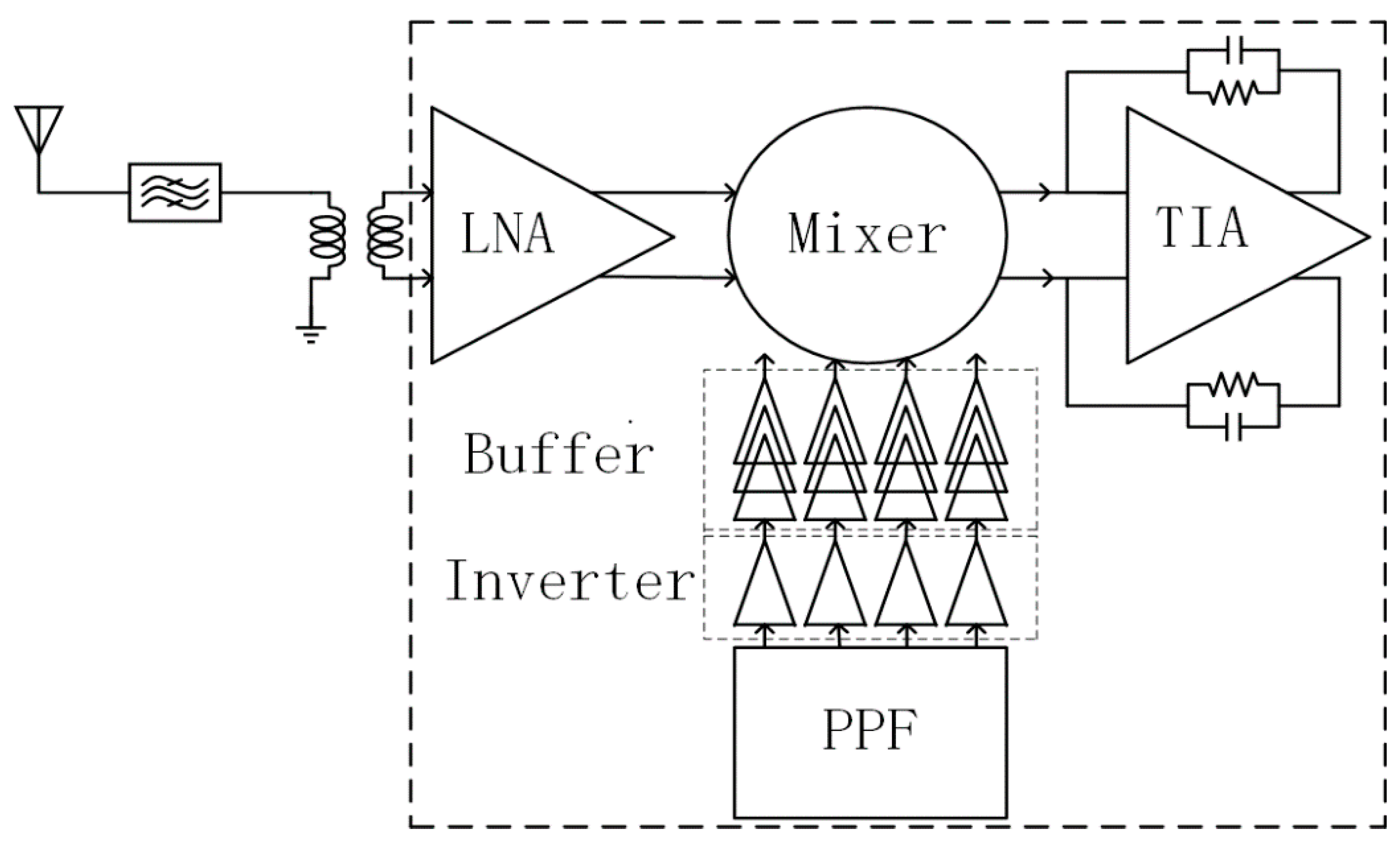
2. Circuit Design
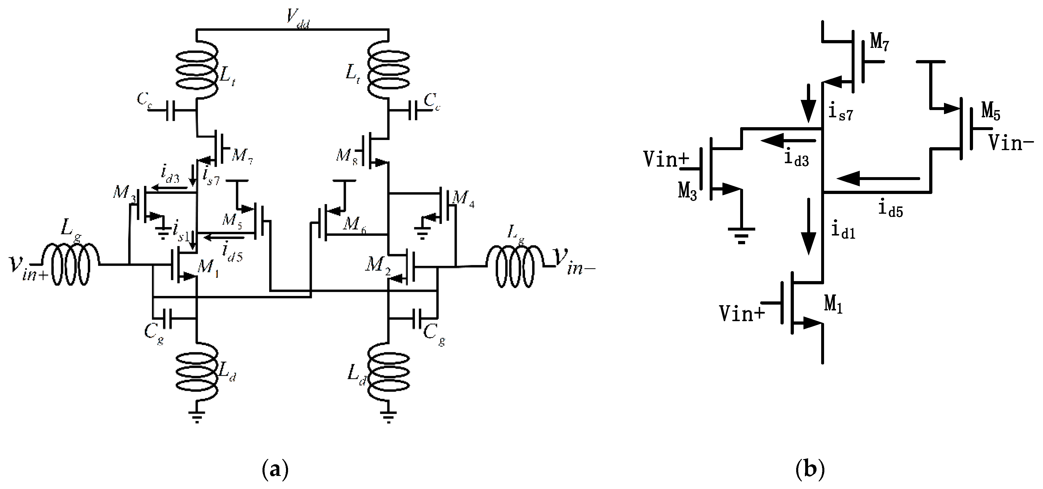
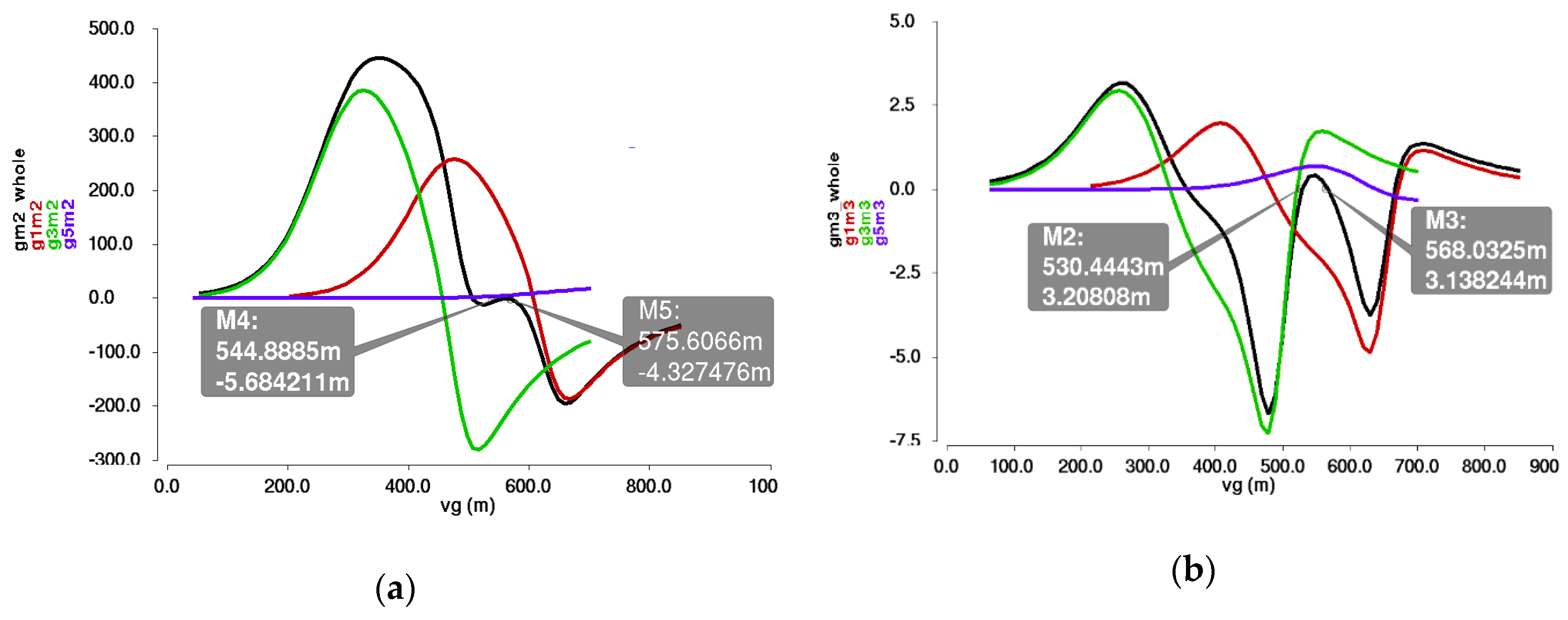
2.1. Proposed LNA Design
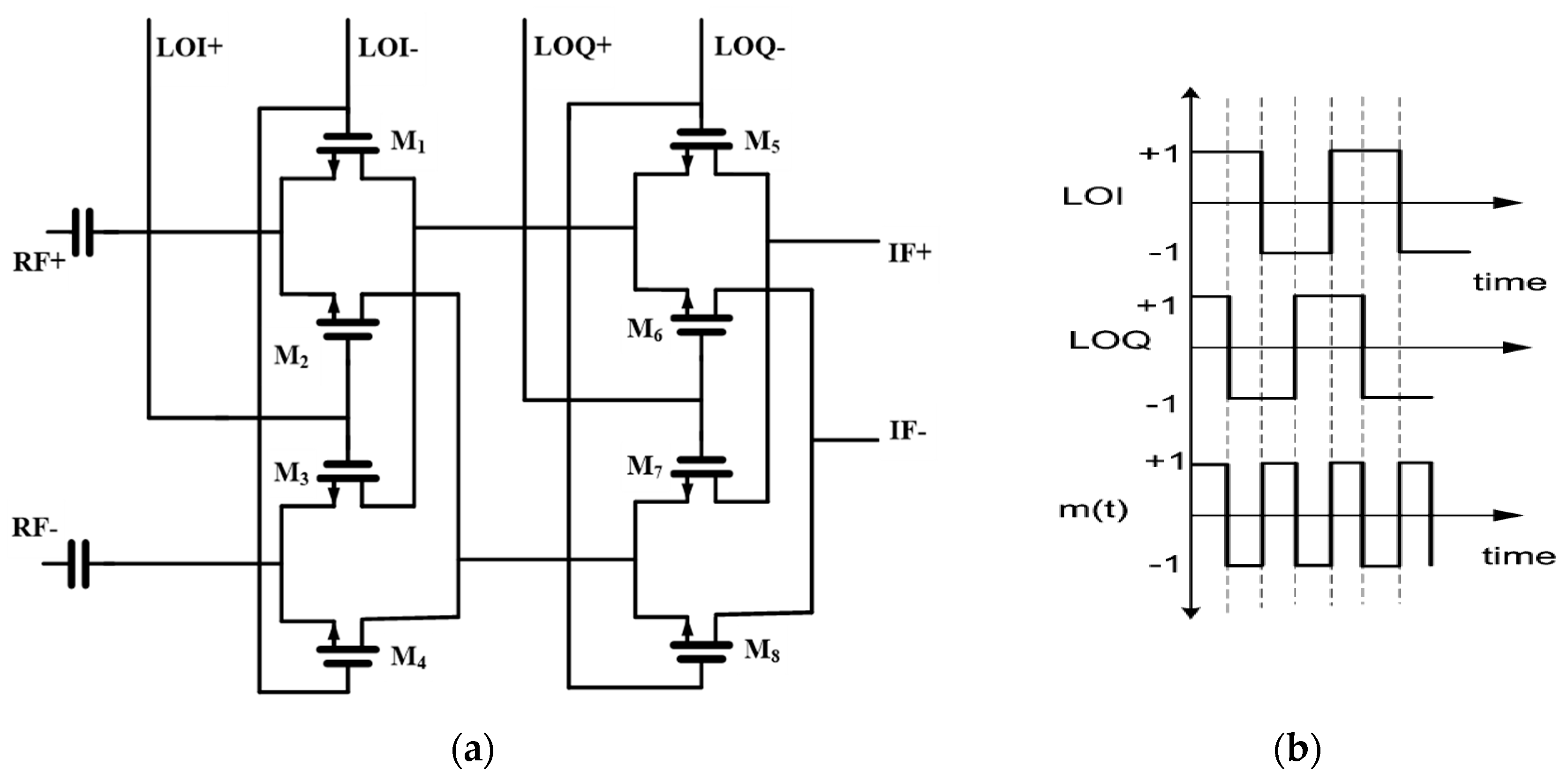
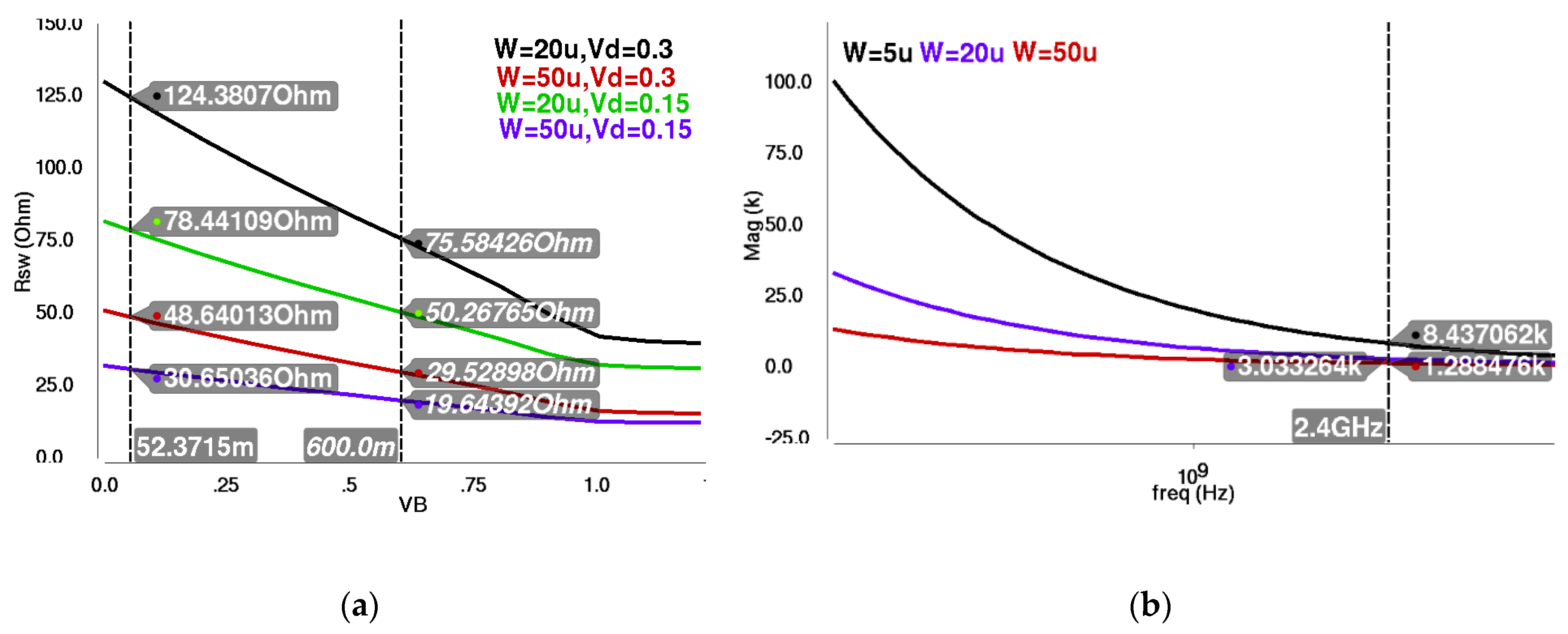
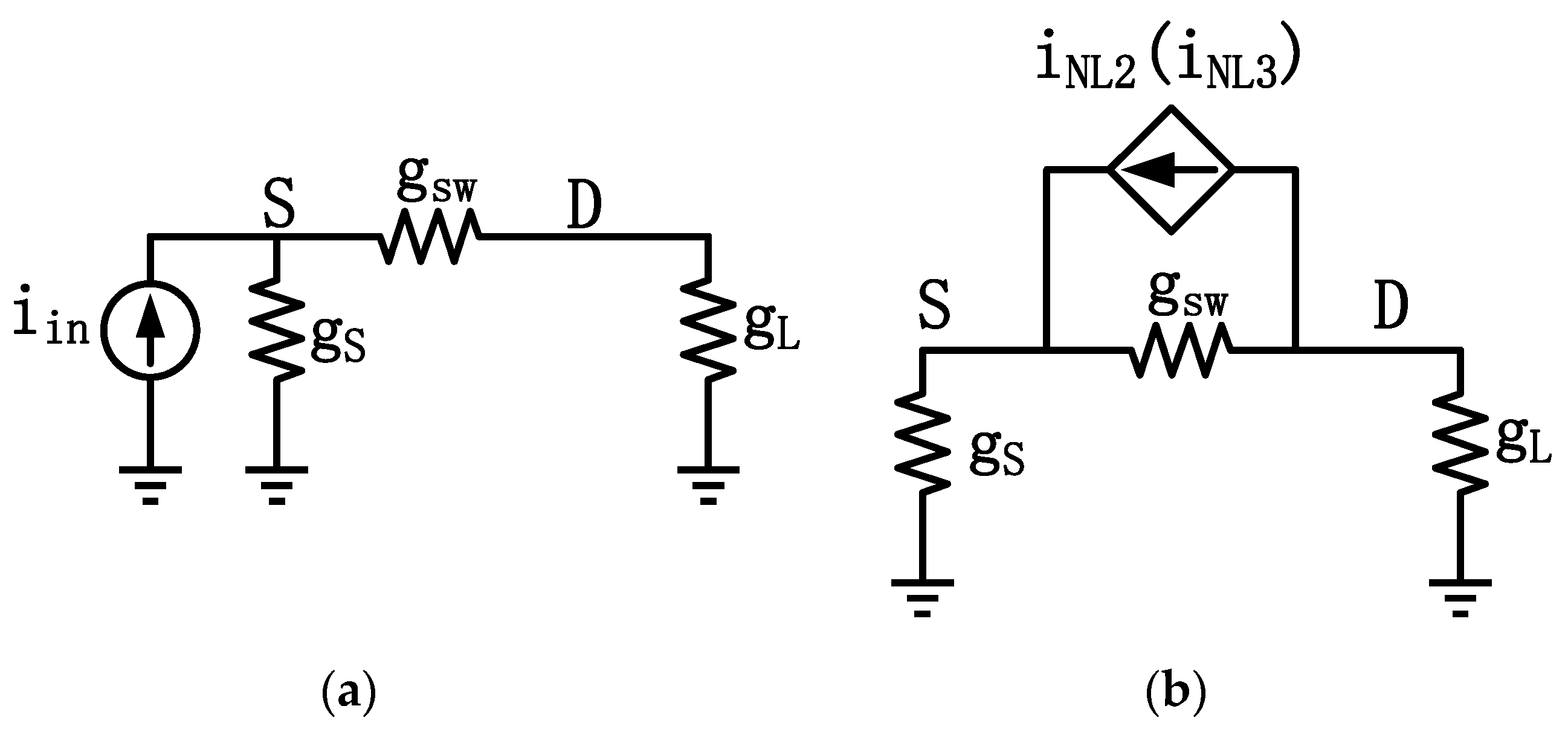
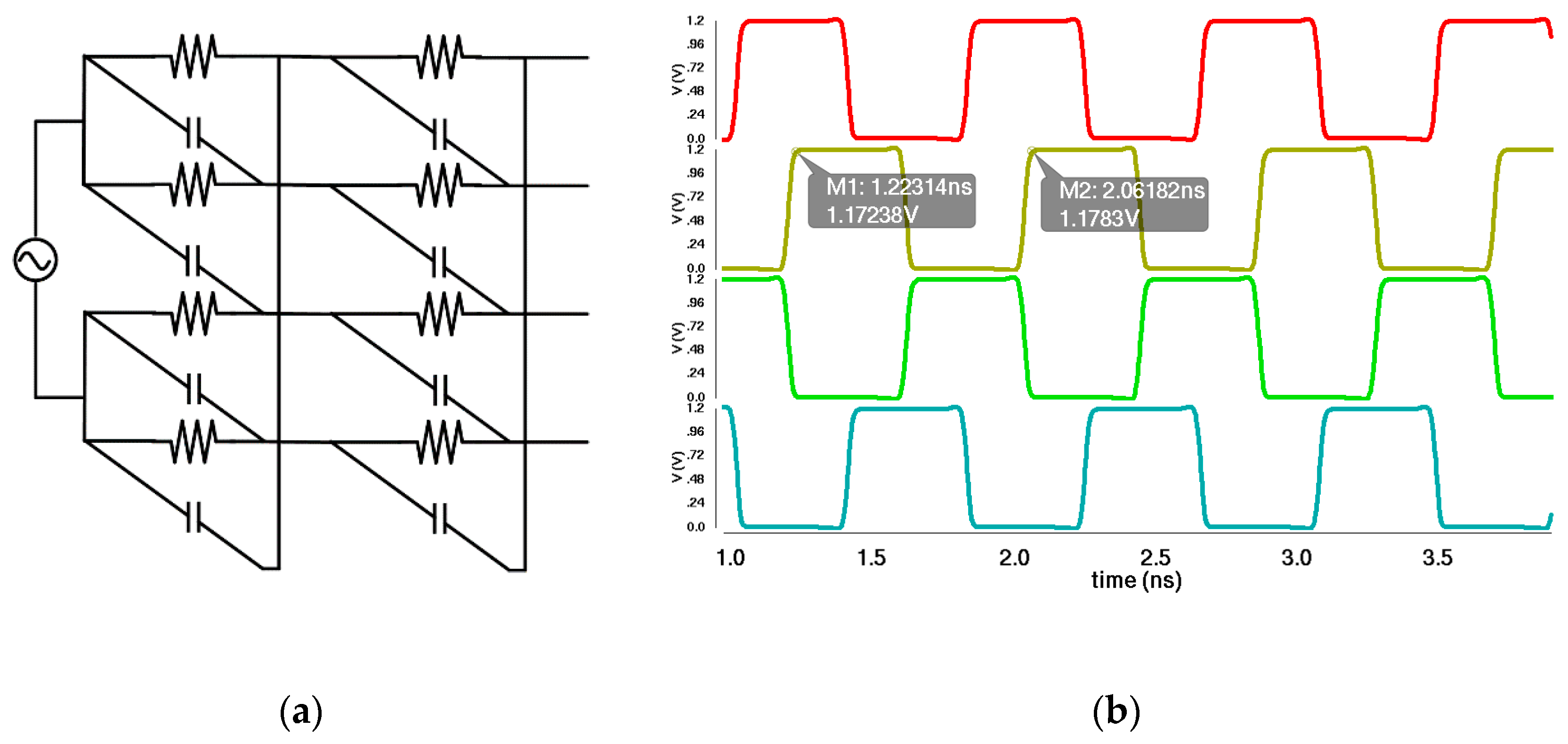
2.2. Current Commutating Subharmonic Passive Mixer Design
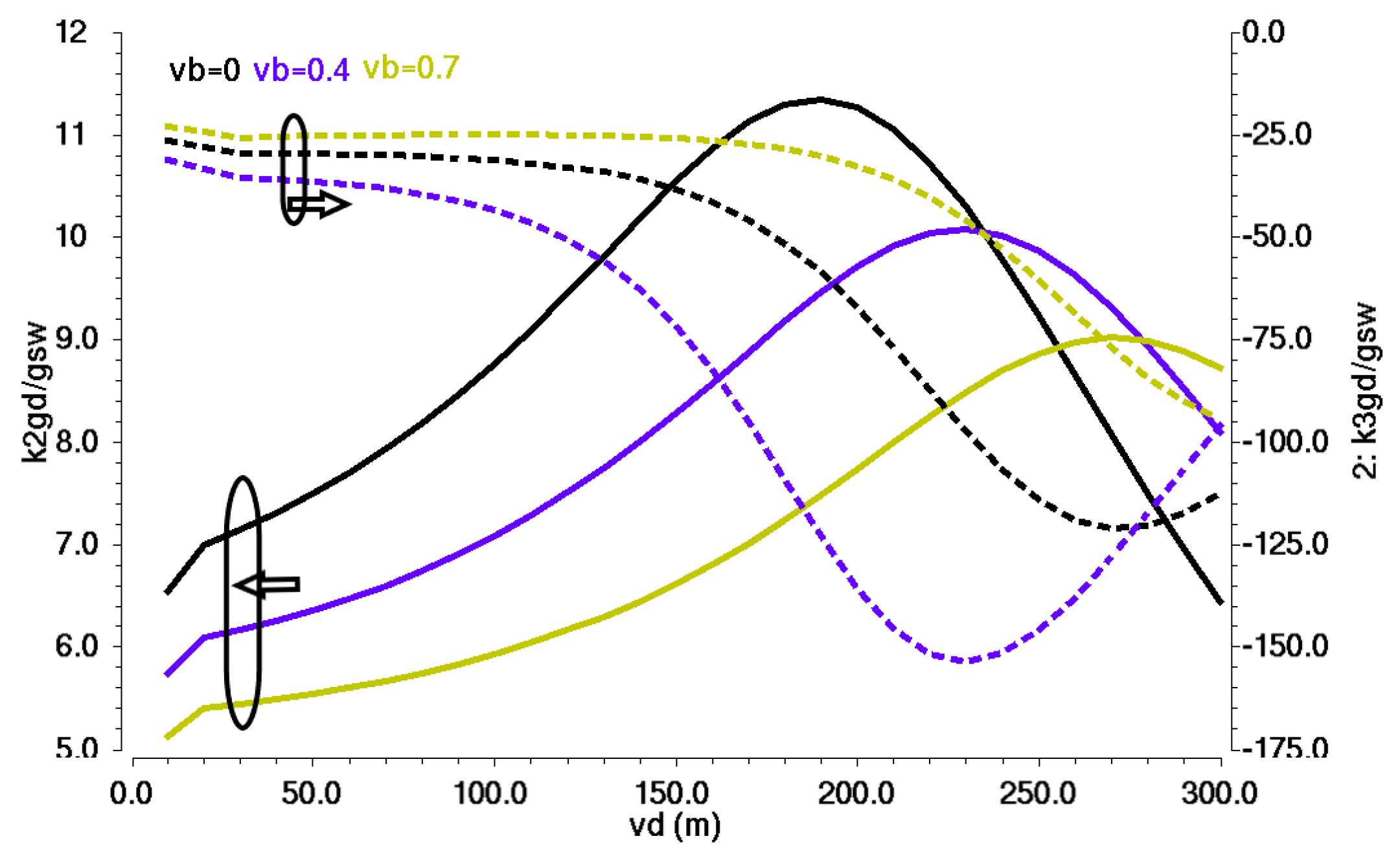
2.3. FBB for Enhancing the Performance of the Mixer Core
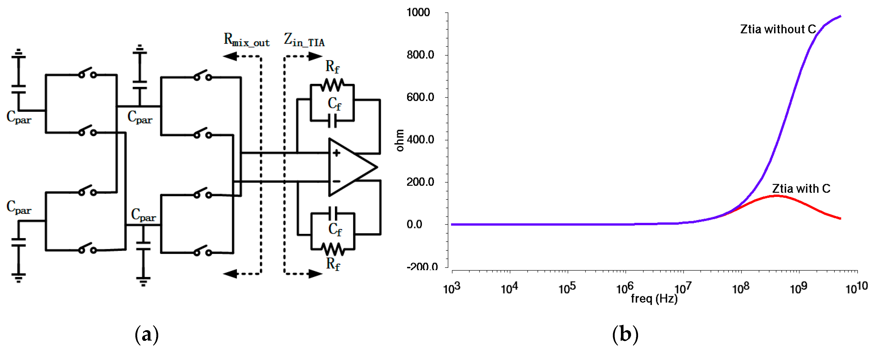
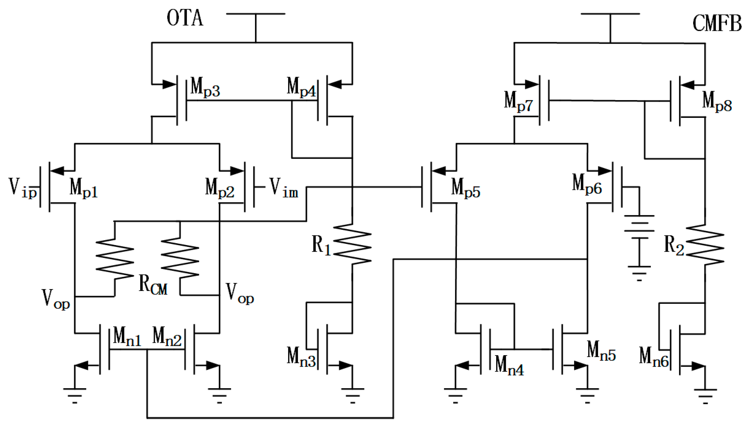
2.4. TIA and Quadrature LO Generation Design
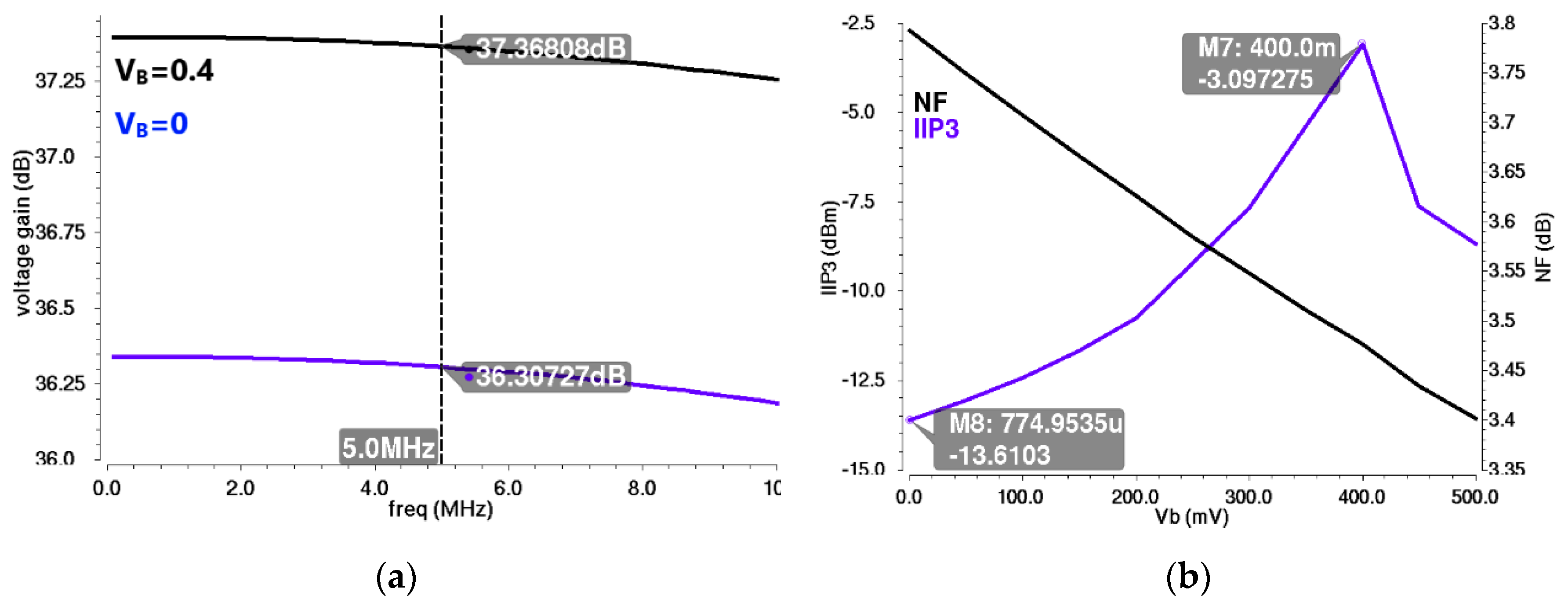
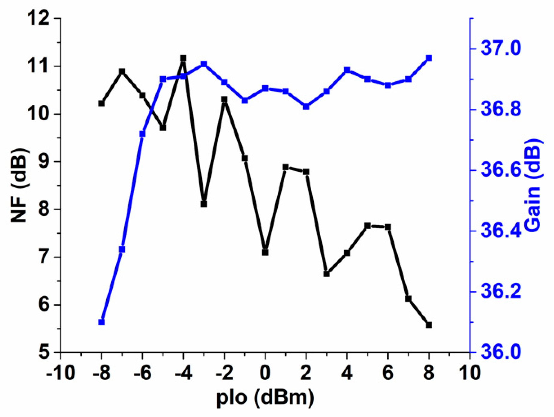
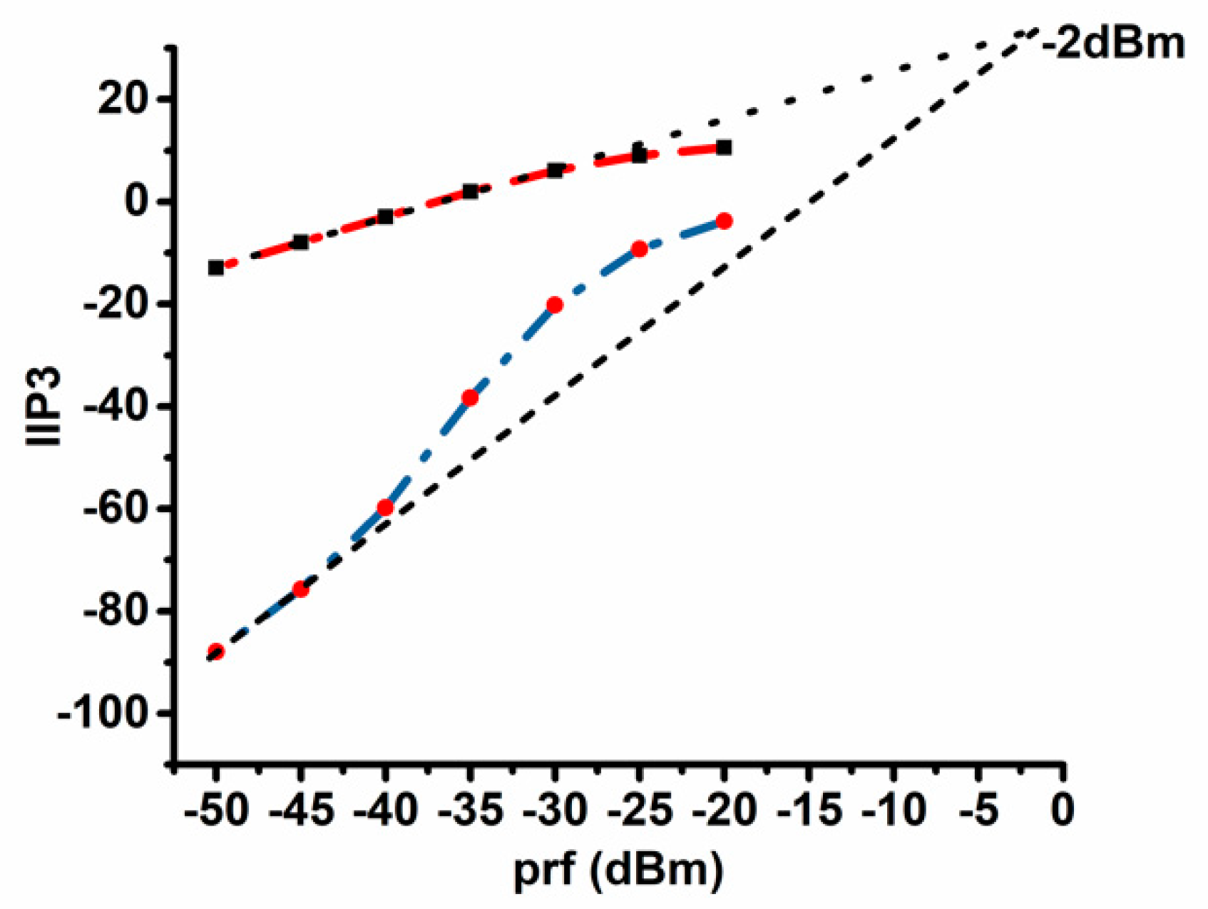
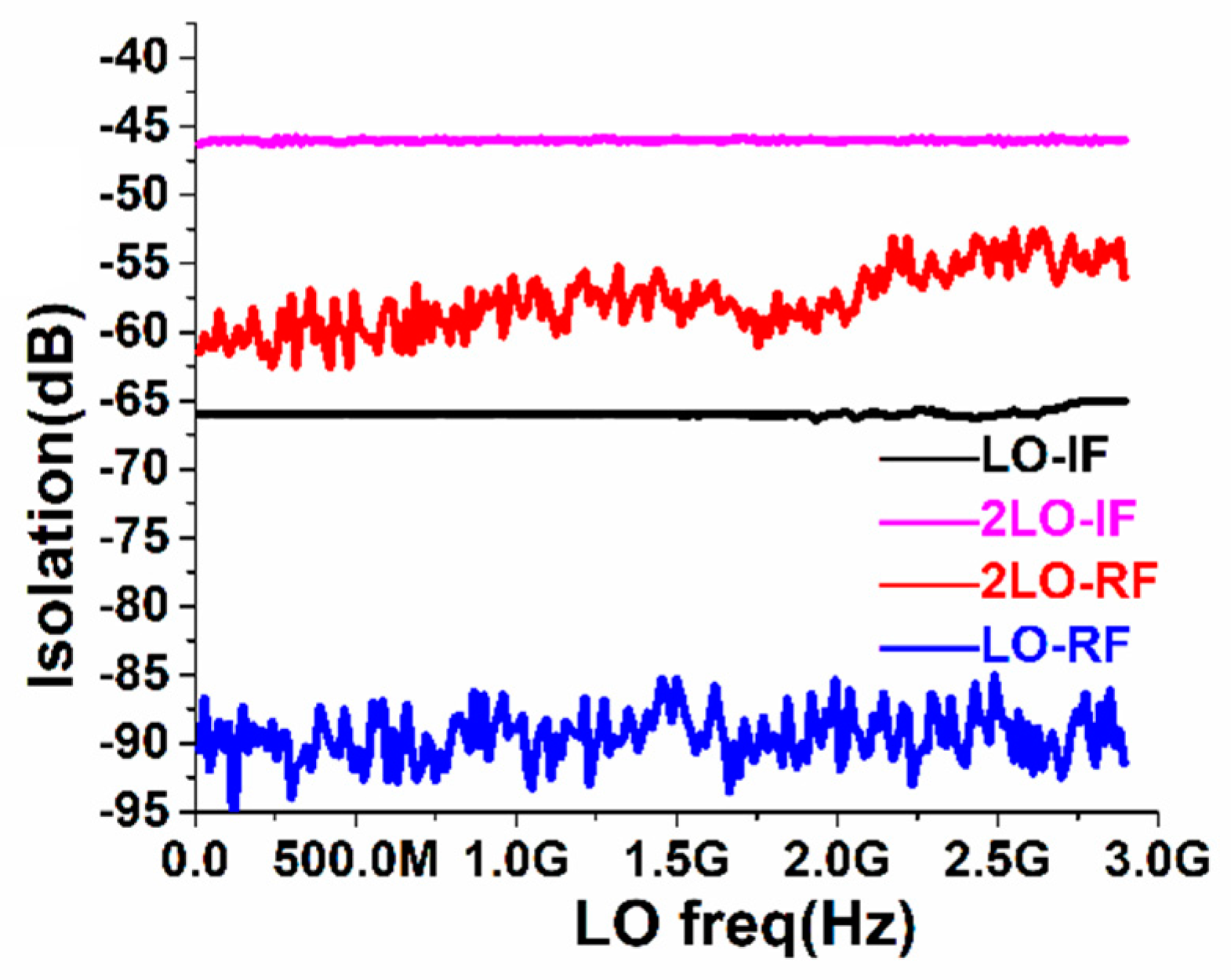
3. Measured Results and Discussion
4. Conclusions
Author Contributions
Funding
Acknowledgments
Conflicts of Interest
References
- Razavi, B. Design considerations for direct-conversion receivers. IEEE Trans. Circuits Syst. II Analog Digit. Signal. Process. 1997, 44, 428–435. [Google Scholar] [CrossRef] [Green Version]
- Koh, K.-J.; Park, M.-Y.; Kim, C.-S.; Yu, H.-K. Subharmonically pumped CMOS frequency conversion (up and down) circuits for 2-GHz WCDMA direct-conversion transceiver. IEEE J. Solid State Circuits 2004, 39, 871–884. [Google Scholar] [CrossRef]
- Luo, T.-N.; Chen, Y.-C.; Yu, Y.-H.; Chen, Y.J.E. A 1-V 900-MHz CMOS Cascaded Even-Harmonic Mixer. In Proceedings of the Asia-Pacific Microwave Conference, Hong Kong, China, 15–19 December 2008; pp. 1–4. [Google Scholar]
- He, S.; Saavedra, C.E. An Ultra-Low-Voltage and Low-Power X2 Subharmonic Downconverter Mixer. IEEE Trans. Microw. Theory Tech. 2012, 60, 311–317. [Google Scholar] [CrossRef]
- Mohamed, S.A.S.; Manoli, Y. Design of Low-Power Direct-Conversion RF Front-End With a Double Balanced Current-Driven Subharmonic Mixer in 0.13 μm CMOS. IEEE Trans. Circuits Syst. I Regul. Pap. 2013, 60, 1322–1330. [Google Scholar] [CrossRef]
- Jin, J. Resonant amplifier-based sub-harmonic mixer for zero-IF transceiver applications. Integration 2017, 57, 69–73. [Google Scholar] [CrossRef]
- Ming-Feng, H.; Kuo, C.J.; Shuenn-Yuh, L. A 5.25-GHz CMOS folded-cascode even-harmonic mixer for low-voltage applications. IEEE Trans. Microw. Theory Tech. 2006, 54, 660–669. [Google Scholar] [CrossRef]
- Syu, J.-S.; Meng, C.; Wang, C.-L. A 2.4-GHz Low-Flicker-Noise CMOS Sub-Harmonic Receiver. IEEE Trans. Circuits Syst. I Regul. Pap. 2013, 60, 437–447. [Google Scholar] [CrossRef]
- Mirzaei, A.; Darabi, H.; Leete, J.C.; Chen, X.; Juan, K.; Yazdi, A. Analysis and Optimization of Current-Driven Passive Mixers in Narrowband Direct-Conversion Receivers. IEEE J. Solid State Circuits 2009, 44, 2678–2688. [Google Scholar] [CrossRef]
- Chehrazi, S.; Mirzaei, A.; Abidi, A.A. Noise in Current-Commutating Passive FET Mixers. IEEE Trans. Circuits Syst. I Regul. Pap. 2010, 57, 332–344. [Google Scholar] [CrossRef]
- Fabiano, I.; Ramella, M.; Manstretta, D.; Castello, R. A +25-dBm IIP3 1.7–2.1-GHz FDD Receiver Front End With Integrated Hybrid Transformer in 28-nm CMOS. IEEE Trans. Microw. Theory Tech. 2017, 65, 4677–4688. [Google Scholar] [CrossRef]
- Xu, Y.; Zhu, J.; Kinget, P.R. A Blocker-Tolerant RF Front End With Harmonic-Rejecting N-Path Filter. IEEE J. Solid State Circuits 2018, 53, 327–339. [Google Scholar] [CrossRef]
- Chong, W.K.; Ramiah, H.; Vitee, N. A 0.12-mm2 2.4-GHz CMOS Inductorless High Isolation Subharmonic Mixer with Effective Current-Reuse Transconductance. IEEE Trans. Microw. Theory Tech. 2015, 63, 2427–2437. [Google Scholar] [CrossRef]
- Modanlou, S.; Miar-Naimi, H.; Gholami, M. Design and analysis of high linearity mixer using subharmonic technique. Int. J. Circuit Theory Appl. 2018, 46, 2202–2216. [Google Scholar] [CrossRef]
- Mollaalipour, M.; Miar-Naimi, H. Design and Analysis of a Highly Efficient Linearized CMOS Subharmonic Mixer for Zero and Low-IF Applications. IEEE Trans. Very Large Scale Integr. Syst. 2016, 24, 2275–2285. [Google Scholar] [CrossRef]
- Kim, N.; Aparin, V.; Larson, L.E. A Resistively Degenerated Wideband Passive Mixer with Low Noise Figure and High IIP2. IEEE Trans. Microw. Theory Tech. 2010, 58, 820–830. [Google Scholar] [CrossRef]
- Tae-Sung, K.; Byung-Sung, K. Post-linearization of cascode CMOS low noise amplifier using folded PMOS IMD sinker. IEEE Microw. Wirel. Compon. Lett. 2006, 16, 182–184. [Google Scholar] [CrossRef]
- Aparin, V.; Larson, L.E. Modified derivative superposition method for linearizing FET low-noise amplifiers. IEEE Trans. Microw. Theory Tech. 2005, 53, 571–581. [Google Scholar] [CrossRef]
- Kodkani, R.M.; Larson, L.E. A 24-GHz CMOS Passive Subharmonic Mixer/Downconverter for Zero-IF Applications. IEEE Trans. Microw. Theory Tech. 2008, 56, 1247–1256. [Google Scholar] [CrossRef]
- Khatri, H.; Gudem, P.S.; Larson, L.E. Distortion in Current Commutating Passive CMOS Downconversion Mixers. IEEE Trans. Microw. Theory Tech. 2009, 57, 2671–2681. [Google Scholar] [CrossRef]
- Chehrazi, S.; Mirzaei, A.; Abidi, A.A. Second-Order Intermodulation in Current-Commutating Passive FET Mixers. IEEE Trans. Circuits Syst. I Regul. Pap. 2009, 56, 2556–2568. [Google Scholar] [CrossRef]
- Chew, K.W.; Zhang, J.; Shao, K.; Loh, W.B.; Chu, S.F. Impact of Deep N-Well Implantation on Substrate Noise Coupling and RF Transistor Performance for Systems-on-a-Chip Integration. In Proceedings of the European Solid-State Device Research Conference, Firenze, Italy, 24–26 September 2002; pp. 2512–2554. [Google Scholar]
- Wambacq, P.; Sansen, W.M. Distortion Analysis of Analog Integrated Circuits; Springer: Boston, MA, USA, 1998. [Google Scholar]
- Sacchi, E.; Bietti, I.; Erba, S.; Tee, L.; Vilmercati, P.; Castello, R. A 15 mW, 70 kHz 1/f Corner direct Conversion CMOS Receiver. In Proceedings of the Custom Integrated Circuits Conference, San Jose, CA, USA, 24 September 2003; pp. 4594–4662. [Google Scholar]
- Kaukovuori, J.; Stadius, K.; Ryynanen, J.; Halonen, K. Analysis and Design of Passive Polyphase Filters. IEEE Trans. Circuits Syst. 2008, 55, 3023–3037. [Google Scholar] [CrossRef]
- Yamaji, T.; Tanimoto, H.; Kokatsu, H. An I/Q active balanced harmonic mixer with IM2 cancelers and a 45° phase shifter. IEEE J. Solid State Circuits 1998, 33, 2240–2246. [Google Scholar] [CrossRef]
- Jen, H.C.; Rose, S.C.; Meyer, R.G. A 2.2GHz Sub-Harmonic Mixer for Directconversion Receivers in 0.13 um CMOS. In Proceedings of the 2006 IEEE International Solid State Circuits Conference—Digest of Technical Papers, San Francisco, CA, USA, 5–9 February 2006; pp. 18401–18849. [Google Scholar]
- Zeng, M.; Huang, R.; Weng, R. A 0.8V 8GHz Low Power Sub-Harmonic Self-Oscillating Mixer. In Proceedings of the 2014 IEEE International Symposium on Circuits and Systems (ISCAS), Melbourne, Australia, 1–5 June 2014; pp. 13761–14379. [Google Scholar]


| Performance Parameters | This Work | [6] | [8] | [13] | [28] | [27] |
|---|---|---|---|---|---|---|
| Process (μm) | 0.13 | 0.18 | 0.18 | 0.13 | 0.18 | 0.13 |
| Topology AM: active mixer; SH: subharmonic | LNA + SHPM + TIA + LO buffer | SHAM | LNA + SHAM | SHAM + SH balun | SHAM + SH LO + IF buffer | LNA + SHPM + LO buffer |
| RF (GHz) | 2.401 | 2.4 | 2.4 | 2.401 | 8 | 2.2 |
| LO (GHz) | 1.2 | - | - | 1.2 | 3.95 | - |
| Supply voltage | 1.2 | 0.8 | 1.8 | 1.2 | 0.8 | 1.2 |
| DC power (mW) | 14.4 | 0.65 | 9 | 5.82 | 9.8 | 12.7 |
| CG (dB) | 36.8 | 14.5 | 31 | 13.6 | 9.4 | 4.5 |
| NF (dB) | 6.8 | 23 | 3 | 20 | 20.9 | 11 |
| IIP3 (dBm) | −2 | 1 | −10 | −4.46 | −3.8 | 0 |
| LO–RF isolation | 90 | 41 | 80 | 65 | 60 | 95 |
| Core size (mm2) | 0.95 | 0.52 | 1.21 | 0.12 | 1.57 | 0.4 |
| FOM | 78.1 | 25.4 | 72.1 | 74.7 | 55.0 | 69 |
© 2020 by the authors. Licensee MDPI, Basel, Switzerland. This article is an open access article distributed under the terms and conditions of the Creative Commons Attribution (CC BY) license (http://creativecommons.org/licenses/by/4.0/).
Share and Cite
Huo, D.; Mao, L.; Wu, L.; Zhang, X. A Linearity Improvement Front End with Subharmonic Current Commutating Passive Mixer for 2.4 GHz Direct Conversion Receiver in 0.13 μm CMOS Technology. Electronics 2020, 9, 1369. https://doi.org/10.3390/electronics9091369
Huo D, Mao L, Wu L, Zhang X. A Linearity Improvement Front End with Subharmonic Current Commutating Passive Mixer for 2.4 GHz Direct Conversion Receiver in 0.13 μm CMOS Technology. Electronics. 2020; 9(9):1369. https://doi.org/10.3390/electronics9091369
Chicago/Turabian StyleHuo, Dongquan, Luhong Mao, Liji Wu, and Xiangmin Zhang. 2020. "A Linearity Improvement Front End with Subharmonic Current Commutating Passive Mixer for 2.4 GHz Direct Conversion Receiver in 0.13 μm CMOS Technology" Electronics 9, no. 9: 1369. https://doi.org/10.3390/electronics9091369
APA StyleHuo, D., Mao, L., Wu, L., & Zhang, X. (2020). A Linearity Improvement Front End with Subharmonic Current Commutating Passive Mixer for 2.4 GHz Direct Conversion Receiver in 0.13 μm CMOS Technology. Electronics, 9(9), 1369. https://doi.org/10.3390/electronics9091369