Abstract
Active inductors are suitable for MMIC integration, especially for filters applications, and the definition of strategies for an efficient design of these circuits is becoming mandatory. In this work we present design considerations for the reduction of DC current in the case of an active filter design based on the use of active inductors and for high-power handling. As an example of applications, the approach is demonstrated on a two-cell, integrated active filter realized with p-HEMT technology. The filter design is based on high-Q active inductors, whose equivalent inductance and resistance can be tuned by means of varactors. The prototype was realized and tested. It operates between 1800 and 2100 MHz with a 3 dB bandwidth of 30 MHz and a rejection ratio of 30 dB at 30 MHz from the center frequency. This solution allows to obtain a P1 dB compression point of about −8 dBm and a dynamic range of 75 dB considering a bias current of 15 mA per stage.
1. Introduction
On-chip passive filters are affected by the limited Q-factor of inductors and capacitors, due to ohmic and substrate losses, even on low-loss substrates as Gallium Arsenide. Tunable passive filters are also affected by the limited Q of varactors, normally used for tunability. Moreover, the bandpass of the filter is affected by the combination of constant passive inductance and variable capacitance in the tuning range. Active filters can be realized with several approaches [1,2,3]; many of them are usually based on active inductors (AIs), that can achieve very low or even negative equivalent resistance, and therefore a high filter Q. The AI can be tuned both in terms of equivalent inductance and of equivalent resistance, yielding constant bandpass with limited losses or positive gain.
In general, active filters usually have limited power handling capabilities also due to the nonlinearities of the active elements, and they are prone to instability due to the negative resistance required for the compensation of the losses of the passive elements in the circuit.
In order to increase the dynamic range, usually a high bias current is required for the active devices. This can lead to higher power consumption that is often unacceptable for integrated circuits and also not allowed at system level. A possible means to reduce the bias current is provided by Class-AB bias, which has already been demonstrated [4]. However, this approach is not always possible or, at least, it experiences some drawbacks depending on the characteristics of the technology process (e.g., the availability of complementary transistors, highly linear active devices).
In this paper, we present a design approach of integrated active inductor and its applications in filters realized in GaAs technology that allows the minimization of bias current, still maintaining Class-A operations that usually ensure high-power handling capability. Concerning the filter AI base design, the proposed approach is based on AIs coupled with shunt capacitors in order to realize an equivalent high-order filter with good performances in terms of shape factor and dynamic range [5,6,7,8]. The topology of the AI is such that only a fraction of the bias current is effectively drawn by the active device and it is useful to provide the required negative resistance. In addition, each cell makes use of a single transistor, reducing power consumption and minimizing possible instability concerns.
An example of application is proposed in MMIC technology, potentially tunable in the frequency range between 1.8 to 2.1 GHz, with a tuning bandwidth of about 15%. The −3 dB bandwidth is almost constant and equal to 30 MHz, while the out-of-band rejection is significant thanks to the high shape factor equal to 2.5 for a 30 dB/3 dB bandwidth ratio. The chip has been designed with a standard process provided by HSRI Foundry that implements 0.13 μm GaAs pHEMT devices. Both simulations and on-chip measurement results are presented with a good agreement between them.
Currently; however, no varactor diodes are available in this technology. Therefore, a fixed-capacitor version was implemented, with different values of the capacitors. In fact, our aim is to provide a feasibility proof demonstrating the tunability capability of the filter by replacing the unavailable varactors with fixed capacitors. A version with the varactors will be implemented and fabricated as soon as the technology is available. However, good performances with varactors have already been demonstrated in a hybrid implementation [5], that indicate the possibility of a successful implementation with varactors also in monolithic technology.
Noise figure has not been considered in this design since noise performance requirements were not so strict in the proposed application (as later discussed); therefore, it is quite high. However, noise reduction techniques have been developed and patented [7] that yield a relatively low noise figure. They will be dealt with in a future publication.
In the following, the topology and principle of operation of the active inductor is briefly summarized in Section 2. Section 2 illustrates also the proposed low-current design approach on an active filter, while in Section 3 the MMIC design and measurement results are shown. Finally, the conclusions are drawn (Section 4).
2. The Active Inductor Architecture
Active filters can be realized by one or more cells, each including an AI-based shunt resonator (Figure 1). Both the shunt capacitor and the AI are tuned in order to maintain both insertion loss and bandpass almost constant across the tuning range. Thus, it is straightforward to notice that the AI is the centerpiece of the filter, as it is also able to control the losses of the cell and; therefore, the overall quality factor of the filter.
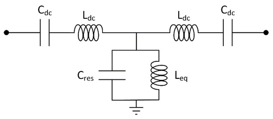
Figure 1.
Topology of a single cell for bandpass active filters.
The traditional structure of the AI is shown in Figure 2a. The input voltage is sampled by a non-inverting transconductance amplifier, that drives a current into the capacitor. The voltage generated in the capacitor is sampled by the inverting transconductance amplifier, that draws an inductive current from the input of the active inductance. The relations between voltages and currents in the active inductor can be better understood in the complex phasor plane (Figure 3). Phases are referred to that of the input voltage Vin. The capacitor voltage VC has a 90 degrees delay (capacitive delay) with respect to the input voltage and the inverting transconductance introduces a further 180° phase shift, so generating an inductive current Iind with respect to the input voltage Vin. An overall excess phase of the output current with respect to the purely inductive 90° phase shift gives an equivalent negative resistance in addition to the equivalent inductance, while an insufficient phase shift gives a positive equivalent resistance. The amplitude of the inductive current with respect to the input voltage determines the value of the equivalent inductance. This amplitude can be changed, for instance, by tuning the value of the transconductance(s).
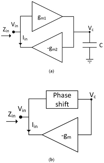
Figure 2.
Active inductor architecture: (a) Traditional topology, (b) improved topology.
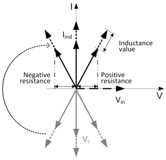
Figure 3.
Phasors of voltages and currents in the AI of Figure 2 in the complex phasor plane. Vin is the input voltage, VC the current across the capacitor (Figure 2a) or at the output of the phase shifting network (Figure 2b), and Iind the current drawn from the inverting transconductance amplifier.3. Low-current design of GaAs active filters based on the proposed AI.
An improved topology of the AI is shown in Figure 2b [5]. The input voltage is sampled at the input of a phase-shifting passive network, then transferred to the input of the inverting transconductance amplifier, that in turn draws the current from the input port. The relations between voltages and currents are approximately the same as in Figure 3; however, some phase shift is also introduced by the inverting transconductance amplifier, given the high operation frequencies. In this improved topology, the amplifier is a fixed-bias, class-A linear amplifier, stable and with fixed gain. The tuning of the phase and amplitude is; therefore, performed by the phase-shifting passive network that includes varactors. This approach allows one to obtain stable and easily tuned AI, and consequently filters with a relatively high gain compression point.
For relatively high-power handling, the current in an AI, conceived with a class-A polarization, may become relatively high. With class-A operation, this requires a high bias current in the active device, where the whole output current flows. A possible means of reducing the DC current is the use of a class-B or class-AB amplifier in the AI [4]. This is certainly a feasible approach that significantly reduces the DC power requirements of the filter, even if it may cause some concerns on intermodulation. However, this approach is not always possible, depending on the characteristics of the active device. For instance, a very sharp pinch-off of the transistor makes the class-B or AB impractical; therefore, a different approach is here proposed and successfully applied to the design of an active filter.
In order to have a high-Q filter, the current at the input of the active inductor must be purely inductive, or nearly so, that is, with a 90 degree phase relation with respect to the voltage across it. The current through a passive inductor has less than 90 degrees with respect to the applied voltage, due to losses. This current can be seen as the vectorial sum of a purely inductive current, and of a purely resistive current in phase with the applied voltage, much smaller in amplitude, due to the losses in the inductor. The compensation of the losses can be obtained by summing another current, opposite in phase with respect to the resistive current and; therefore, equivalent to the current of a negative resistance. This negative resistance current will be therefore much smaller than the total current in the inductor.
A possible topology that implements this approach is shown in Figure 4. The current from the input of the AI flows through a passive inductor (IL in Figure 4), because the capacitive current that enters the gate of the active device is relatively small and can be neglected. Then, the main part of this current (Ipassive in Figure 4) flows through a relatively large capacitor Cg, that has a smaller impedance compared to the passive inductor. Therefore, this current is mainly inductive with respect to the input voltage, but also has a resistive component, due to the losses in the capacitor and in the inductor. From the plot in Figure 5 its resistive nature is apparent from its phase relation to the input voltage.
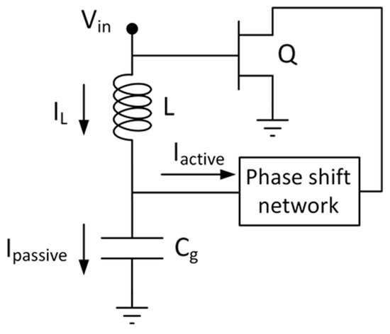
Figure 4.
Improved topology of the AI for class-A low bias current.
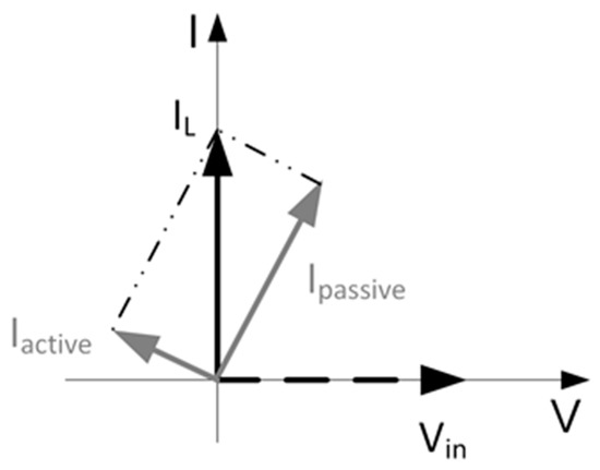
Figure 5.
Phasors of voltages and currents in the AI of Figure 3 in the complex plane. Vin is the input voltage, IL the current through the inductor L. Ipassive is the current through the capacitor Cg and Iactive the current drawn from the transistor through the phase-shifting network. Their vectorial sum gives the current through the inductance IL.
A smaller part of the current through the passive inductor flows through the phase-shifting network (Iactive in Figure 4). This current can have a negative resistance component with respect to the input voltage, because it ultimately comes from the active device. The size of the active device, and the delay introduced by the phase-shifting network must be designed in such a way, that the negative-resistance component of the Iactive current compensates the resistive component of the Ipassive current through the capacitor. In this way its amplitude is kept to a low value compared to the total current flowing into the AI. Therefore, the current through the active device is minimized, compared to the standard design, where all the current flowing into the AI comes from the active device. As a consequence, bias current and overall power consumption in minimized.
The value of the equivalent inductance is easily tuned by varying the value of the capacitance Cg, that can be implemented with a varactor; given the relatively high value of the capacitor, the series L - Cg is inductive, because the operating frequency is higher than the resonant frequency of the LC series. By changing the value of the capacitor, also the equivalent inductance of the LC series is varied. Another varactor can be used also to implement the resonating capacitance Cres of the single cell (Figure 1). The simultaneous tuning of the resonating capacitance and of the equivalent inductance yields a constant bandpass across the tuning frequency range, while the low losses or possibly small negative equivalent resistance of the AI allow to enhance the Q-factor of the filter.
The proposed design approach has some similarities with the negative impedance converter (NIC) approach [9,10]. However, the negative resistance is not designed as a one-port, additive network, but is obtained by suitable phasing of the active inductor loop. Moreover, the very simple AI topology here addressed, based on a single transistor per cell, greatly reduces the current requirements, and makes stability enforcement quite straightforward, ensuring at the same time also high-power handling together with low-power consumption.
When properly implemented, the proposed approach does not cause any reduction in the tuning range or increase in losses with respect to the traditional approach. The main result is the reduction of the current required from the active device, with consequent increase of power handling with the same active device.
It is also important to notice that the proposed design approach is not based on equations but on the optimization of network parameters (currents, voltages, equivalent impedances) at both small and large signals. It suggests a suitable architecture for the realization of active filters based on active inductors. An analytical approach is hard to realize since the filter makes use of AIs that are implemented as closed loop circuits. In addition, it is not useful from a practical point of view also considering that at these frequencies circuits usually make use of distributed elements that are difficult to analytically describe. So the description is strictly related to the network configuration and cannot be generalized.
3. MMIC Design and Test
Following the above proposed design strategy and making use of the new architecture shown in Figure 4 for the AI, a two-cells example filter has been designed, considering for each cell the same architecture shown in Figure 1. However, the core of the proposed work is the AI design and the filter performance are strictly dependent on the active inductor characteristics. The AI should be applied also to different filter families (e.g., Butterworth, Chebyshev, etc.) [11] that make use of grounded inductors. In this example, the filter has been fabricated on a GaAs technology provided by HSRI, realized and tested for demonstration. The standard PDK from HSRI includes 0.13 μm pHEMT devices that exhibit low noise figure, high gain and high-power density (0.7 W/mm). Varactor diodes are not currently available in this technology; the design will be updated with inclusion of varactors as soon as they are available in the future. The proposed design method can be applied with any technology process and into the millimeter-wave band. It is also important to note that the performances of the example filter have been designed for the replacement of an existing passive filter used as post selector in base station unit for mobile communications, and so could be improved further.
The filter acts exactly as a resonator. Its ease of realization represents its effectiveness. More in detail, Cres and Lres in Figure 1 define the resonant frequency, that is the center frequency of the filter. The quality factor of the filter depends mainly on the quality factors of the components used in the resonator. Cdc and Ldc realize series resonators that have decoupling effects and are helpful to tighten the filter bandwidth. The same architecture has been widely described in [11,12,13]. The filter has been realized replying twice the same cell. Each single cell includes an active inductor that realizes Lres. The embedded AI in each cell has been realized with a transistor, whose dimensions are 6 × 25 um, in common source configuration. A self-gate bias architecture has also been implemented in order to limit the number of the bias pads and to reduce the temperature dependence of the filter characteristics. The bias current per transistor is 15 mA, while the total power consumption is 120 mW with a DC voltage supply of 4 V. It is straightforward to notice that the DC power consumption is not very low; but in this example this design choice was not critical. In general, it depends on the desired linearity and dynamic range of the filter, in addition to the available technology. Considering the HAMLA13B Model Handbook from HSRI, in particular the recommended bias voltages and the IV-curves of the active devices, a drain voltage of 4 V and a bias current per transistor of 15 mA are suitable choices, considering the required power handling and the connected voltage and current swings. Obviously, by using different technology processes and considering different design specs power consumption should be different, but still in the same order of magnitude if you use the same transistor topology. In addition, it may be reduced also changing the number of cells, so allowing to have a lower shape factor of the filter.
In Figure 6, the complete schematic of the single cell is reported, while in Figure 7, the simulated results of the proposed IC design are shown for a fixed tuning state. The insertion loss is about 6 dB, while the 3 dB bandwidth is 30 MHz. It is worth noting that given the active nature of the filter there is no problem in principle to obtain very low attenuation, close to zero, but this was not the aim of this work since the proposed circuit has been designed for the one-to-one replacement of an existing passive post-selector filter, and therefore it had to have the same performances. In that application the insertion loss is not a critical parameter, and has not been improved. However, active filters may reduce the attenuation to zero or even have amplification, at the expense of stability. Typically, an insertion loss of 0.5 dB can be reached with still a good stability margin. The insertion loss is defined properly balancing the negative resistance introduced by the active inductor and losses of passive components of filtering network. So, it is of primary importance the definition of a suitable shape for the input impedance of the AI that allows to provide low losses, out-of-band rejection and tunability versus an external control voltage. As shown in Figure 7, the shape factor achievable with the proposed solution is typical of higher-order passive solutions [11], and the quality factor is approximately equal to 90. It is important to remark that the circuit is stable, as evident from the behavior of the stability factor K and Delta parameter in the same figure [14]. The stability has been checked not only between the external RF I/O pads, but also at transistor level in each stage with the approach proposed in [8]. This is necessary due to the presence of feedback networks (Figure 4) that may generate inner instability problems. In particular, the amplifier in each active inductor is unconditionally stable at all frequencies. Additionally, each cell is unconditionally stable at all frequencies, because the small negative resistance of the active inductor is compensated by the losses of the resonating capacitor and of the connecting lines. Therefore, no oscillations can take place due to reflections between cells. In Figure 8, the simulated output power and attenuation vs. input power are shown for the circuit tuned at 1800 MHz, for a −7 dBm compression point. In Figure 9, the simulated dynamic load lines of the transistor for the same tuning frequency are also shown for several input power levels, demonstrating class-A operations.
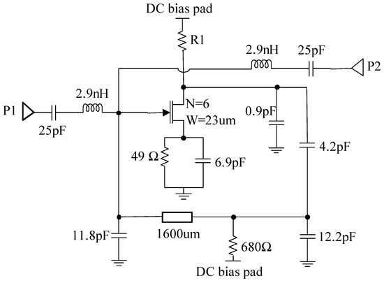
Figure 6.
Schematic of the single cell.
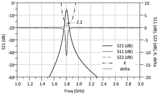
Figure 7.
Simulated S-parameters and stability parameters of the two-cell filter for a single frequency.
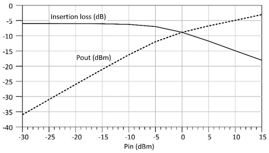
Figure 8.
Simulated compression of the filter tuned at 1800 MHz.
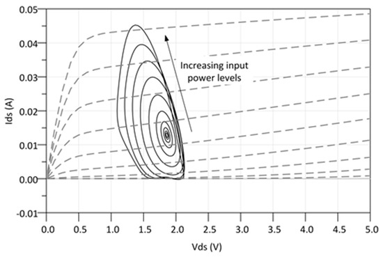
Figure 9.
Dynamic load line of the transistor of the filter tuned at 1800 MHz, for different input power levels up to −9 dBm.
At the considered frequencies, better performance can be achieved by using, for instance, SAW devices. However, SAW filters [15] have a limited integration capability and cannot be used at very high frequencies. Additionally, an active chip filter has potential tunability, and smaller size and cost compared to a SAW filter.
A photograph of the fabricated chip is shown in Figure 10a. The chip size is 3 × 1.5 mm, and obviously may be further reduced in next redesign. The two cells are coupled by LC-series elements. The single cell is magnified in Figure 10b, where also some voltages and currents components are reported to better illustrate the proposed approach.
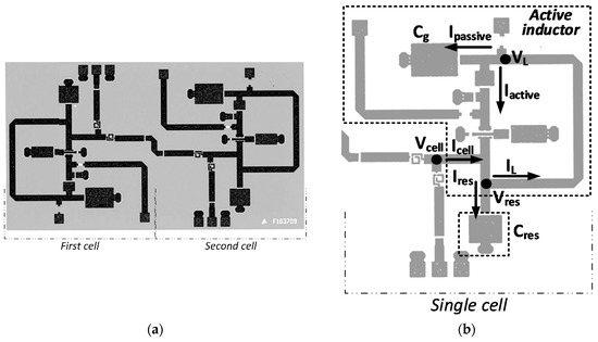
Figure 10.
The fabricated active filter: (a) Photograph of the chip, (b) a single cell where the currents of Figure 4 are indicated.
The behavior of the same electrical parameters is shown in the follows in order to prove the design consideration introduced in the previous Section. The main inductance L in Figure 4 in this example is replaced by a length of line in each cell. Since standard PDK from HSRI does not include varactors, it has not been possible to use variable capacitors, so in this first run they have been replaced by fixed capacitances, for a first assessment of the design approach and in order to avoid further uncertainties that may be introduced by the nonlinear models of the devices. In fact, our aim is to provide a feasibility proof demonstrating the tunability capability of the filter by replacing the unavailable varactors with fixed capacitors. So, three different chips with different capacitance values of the capacitor Cg in Figure 10b have been fabricated, each tuned to a different center frequency. However, the values of the fixed capacitances have been designed with a capacitance ratio of 3:1 for the full tuning bandwidth, making them suitable to be replaced by real varactors. Obviously, there are minor adjustments to be made when the fixed capacitors are replaced by varactors, mainly in term of losses. But we have already verified in different discrete prototypes that the replacement is still possible and does not significantly affect the overall performance of the filter. This is possible thanks to the active nature of the inductors, that can be slightly tuned to compensate the additional losses introduced by varactors.
In Figure 11, comparison between simulated and measured S-parameters for a fixes tuning state is reported demonstrated a good agreement; while measured results of the S-parameters of the three chips, centered at the center frequency and at the two extreme frequencies in the tuning range, are reported in Figure 12. As shown, bandwidth and quality factor are approximately constant at all frequencies. The currents in the active inductor and the corresponding voltages, as indicated in Figure 10b, are plotted in Figure 13, Figure 14 and Figure 15 vs. time. All quantities refer to the cell tuned at 1800 MHz and at compression level. More in details, in Figure 13 the voltage (Vcell) and current (Icell) at the input of the cell are shown. It is apparent that the cell has resistive behavior, but very low losses, as indicated by the very low current. In Figure 14 the currents (Ires) in the resonating capacitance and in the active inductance (IL) are shown, together with the voltage at that node (Vres). The sum of the two currents (Ires and IL) is almost zero since they are in anti-phase, indicating their almost total cancellation. In Figure 15, the inductor current IL, the current Ipassive through the capacitor Cg and the current Iactive from the transistor are shown, together with the voltage at the corresponding node. As stated in the previous section, it is apparent that also in this example the main contribution of the inductor current flows through the capacitor Cg to ground, and that it is a passive current, as indicated by the phase relation between voltage and current.
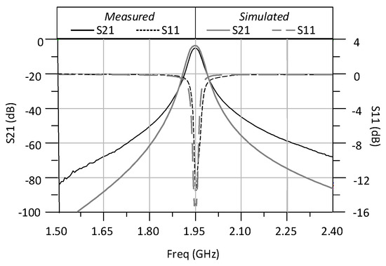
Figure 11.
Comparison between simulated and measured S-parameters at center frequency.
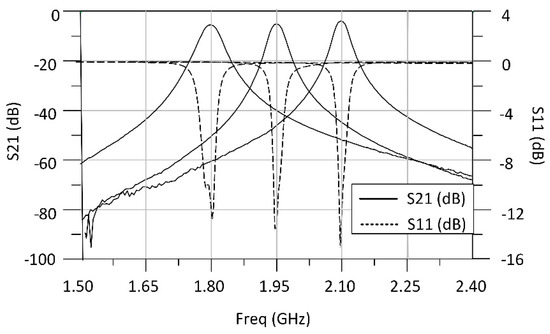
Figure 12.
Measured S-parameters of the two-cell filter at three frequencies in the tuning range.
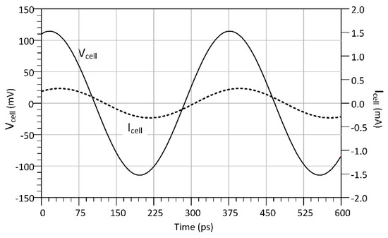
Figure 13.
Simulated voltage and current at the input of the resonating cell (see Figure 10b).
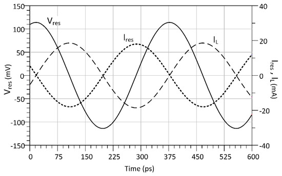
Figure 14.
Simulated currents IRES in the resonating capacitance CRES and in the active inductor IL, together with the voltage VRES at the corresponding node (see Figure 10b).
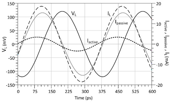
Figure 15.
Simulated voltage and current at the input of the resonating cell (see Figure 10b).
A minor contribution comes from the transistor, and it is an active current. Their combination is a slightly active current, corresponding to a negative equivalent resistance, that compensates for the losses in the resonator capacitance (Cres). Thus, these real waveforms illustrate and confirm the design approach represented in Figure 4 and Figure 5, that minimizes the RF current in the transistor and; therefore, the bias current requirement for the transistor itself.
The noise figure of the filter has not been measured, since it was not optimized in this design. Simulations give a noise figure in the order of 12 dB. However, reduction techniques [6] should reduce it to approximately 8 dB, approaching the noise figure of a filter with similar losses. Noise reduction techniques will be specifically addressed in a successive design.
It is also important to notice that in the proposed design example of Figure 6, passive components are optimized for the considered frequency and they change accordingly to the operational bandwidth. In any case, as showed in the layout photograph of Figure 10 the area waste due to both the number of components and their values is minimal; in addition some passive components can be also replaced by distributed elements moving at higher frequencies, so further reducing the chip area. In general, the same networks definition may change moving the design to different frequencies, since it strictly depend also on the technology and specs, but still preserving around the same area occupation and realizing the same design principle illustrated in Figure 4. The proposed design is also robust towards tolerances and spread effects. It has been verified also measuring different chips and all of them show similar performance. So the design choices allow to obtain a good reliability making the filter a good candidate to be used in practical applications.
Finally, for completeness, in Table 1 a summary of measurement results is also presented. Both linear and nonlinear characteristics are in good agreement with simulations, showing the feasibility and reliability of the proposed IC design. Table 2 shows also a comparison with different literary solutions. From Table 2 it is evident that this work has the highest power consumption, but it is important to notice that the power consumption mainly depends on the selected technology. In the same table, almost all the cited works are realized with CMOS technologies; while just one work makes use of a p-HEMT technology. Obviously, the power consumption of MOS technologies is significantly lower; but on the opposite this kind of technologies cannot provide proficient results at higher frequencies, mainly in term of power handling capability and tunability. The power consumption of the reference makes use of p-HEMT technology around one half (so on the same order of magnitude) of that shown by our work, but it has also a P−1 dB compression point significantly lower. A higher power consumption is usually necessary to obtain better power handling capability. Our work is not strictly focused on performance, but it should be considered as a proof-of-concept and demonstrates the reliability of the proposed design approach. By using HEMT devices, the same design scheme should be successfully applied at also tens of GHz, ensuring good tunability and high 1 dB power compression point.

Table 1.
Summary of measured results.
Table 2.
Comparison with different literary solutions.
4. Conclusions
We presented an innovative design approach for the minimization of the bias current in the AI-based active filters. The design strategy here proposed allows to obtain a significant reduction of the required DC power, without significantly affecting the power handling capability. The core of the solution here addressed for the first time is the active inductor design. Both the circuitry architecture and the components values were optimized to this purpose and the design choices were described in detail. We also showed how the equivalent inductance and resistance can be tuned by means of variable capacitances. An example of application was also provided: An integrated active filter, centered at three different frequencies, was realized with pHMET technology provided by HSRI Foundry. The filter was optimized between 1800 and 2100 MHz with a narrow and almost constant 3 dB bandwidth of about 30 MHz and a high shape factor, typical of higher order passive filters. This solution allows one to obtain a dynamic range of about 75 dB, minimizing the power consumption. All these characteristics, as well as measured results, makes the proposed solution a good candidate to be used in practical applications and many RF TX/RX systems.
Author Contributions
Conceptualization, G.L., V.S. and L.P.; investigation, L.P. and V.S.; data curation, H.L. and Z.H.; supervision, G.L.; validation, H.L.; writing and editing, L.P., G.L. and V.S. All authors have read and agreed to the published version of the manuscript.
Funding
This research received no external funding.
Conflicts of Interest
The authors declare no conflict of interest.
References
- Aghazadeh, S.; Martinez, H.; Saberkari, A. 5 GHz CMOS All-Pass Filter-Based True Time Delay Cell. Electronics 2018, 8, 16. [Google Scholar] [CrossRef]
- Safari, L.; Barile, G.; Ferri, G.; Stornelli, V. High performance voltage output filter realizations using second generation voltage conveyor. Int. J. RF Microw. Comput. Aided Eng. 2018, 28, e21534. [Google Scholar] [CrossRef]
- Ben Hammadi, A.; Haddad, F.; Mhiri, M.; Saad, S.; Besbes, K. RF and Microwave Reconfigurable Bandpass Filter Design Using Optimized Active Inductor Circuit. Int. J. RF Microw. Comput. Aided Eng. 2018, 28, e21550. [Google Scholar] [CrossRef]
- Thanachayanont, A.; Sae Ngow, S. Class AB VHF CMOS active inductor. In Proceedings of the 2002 45th Midwest Symposium on Circuits and Systems, 2002, MWSCAS-2002, Tulsa, OK, USA, 4–7 August 2002. [Google Scholar]
- Pantoli, L.; Stornelli, V.; Leuzzi, G. Tunable active filters for RF and microwave applications. J. Circuits Syst. Comput. 2014, 23, 1450088. [Google Scholar] [CrossRef]
- Pantoli, L.; Stornelli, V.; Leuzzi, G.; Hongjun, L.; Zhifu, H. GaAs MMIC tunable active filter. In Proceedings of the 2017 Integrated Nonlinear Microwave and Millimetre-wave Circuits Workshop (INMMiC), Graz, Austria, 20–21 April 2017. [Google Scholar]
- Pantoli, L.; Stornelli, V.; Leuzzi, G. Low-noise tunable filter design by means of active components. Electron. Lett. 2016, 52, 86–88. [Google Scholar] [CrossRef]
- Pantoli, L.; Stornelli, V.; Leuzzi, G. A low-voltage low-power 0.25 µm integrated single transistor active inductor-based filter. Analog Integr. Circuits Signal Process. 2016, 87, 463–469. [Google Scholar] [CrossRef]
- Foster, R. A Reactance Theorem. Bell Syst. Tech. J. 1924, 3, 259–267. [Google Scholar] [CrossRef]
- Merrill, J. Theory of the Negative Impedance Converter. Bell Syst. Tech. J. 1951, 30, 88–109. [Google Scholar] [CrossRef]
- Zverev, A.I. Handbook of Filter Synthesis; John Wiley & Sons: New York, NY, USA, 1967. [Google Scholar]
- Rhea, R.W. Filter Synthesis Using Genesys S/Filter; Artech House Publishers: Boston, MA, USA, 2014. [Google Scholar]
- Matthaei, G.L.; Young, L.; Jones, E.M. Microwave Filters. Impedance Matching Networks and Coupling Structures; Artech House Books: Boston, MA, USA, 1980. [Google Scholar]
- Platzker, A.; Struble, W.; Hetzler, K.T. Instabilities diagnosis and the role of K in microwave circuits. In Proceedings of the IEEE MTT-S International Microwave Symposium Digest, Atlanta, GA, USA, 14–18 June 1993; Volume 3, pp. 1185–1188. [Google Scholar]
- Lu, X.; Mouthaan, K.; Soon, Y.T. Wideband Bandpass Filters With SAW-Filter-Like Selectivity Using Chip SAW Resonators. IEEE Trans. Microwave Theory Tech. 2014, 62, 28–36. [Google Scholar] [CrossRef]
- Mohammadi, L.; Koh, K. 2–4 GHz Q-tunable LC bandpass filter with 172-dBHz peak dynamic range, resilient to +15 dBm out-of-band blocker. In Proceedings of the 2015 IEEE Custom Integrated Circuits Conference (CICC), San Jose, CA, USA, 28–30 September 2015. [Google Scholar]
- Mohammadi, L.; Koh, K. Low power highly linear band-pass/band-stop filter for 2–4 GHz with less than 1% of fractional bandwidth in 0.13 µm CMOS technology. In Proceedings of the 2017 IEEE Radio Frequency Integrated Circuits Symposium (RFIC), Honolulu, HI, USA, 4–6 June 2017. [Google Scholar]
- Kumar, V.; Mehra, R.; Islam, A. A 2.5 GHz Low Power, High-Q, Reliable Design of Active Bandpass Filter. IEEE Trans. Device Mater. Reliab. 2017, 17, 229–244. [Google Scholar] [CrossRef]
- Wu, B.; Chiu, Y. A 40 nm CMOS Derivative-Free IF Active-RC BPF With Programmable Bandwidth and Center Frequency Achieving Over 30 dBm IIP3. IEEE J. Solid-State Circuits 2015, 50, 1772–1784. [Google Scholar] [CrossRef]
- Wang, S.; Lin, W. C-band complementary metal-oxide-semiconductor bandpass filter using active capacitance circuit. IET Microw. Antennas Propagat. 2014, 8, 1416–1422. [Google Scholar] [CrossRef]
- Fan, K.W.; Weng, C.C.; Tsai, Z.M.; Wang, H.; Jeng, S.K. K-band MMIC active band-pass filters. IEEE Microw. Wirel. Compon. Lett. 2005, 15, 19–21. [Google Scholar]
- Chaturvedi, S.; Božanić, M.; Sinha, S. 60 GHz BiCMOS active bandpass filters. Microelectron. J. 2019, 90, 315–322. [Google Scholar] [CrossRef]
© 2020 by the authors. Licensee MDPI, Basel, Switzerland. This article is an open access article distributed under the terms and conditions of the Creative Commons Attribution (CC BY) license (http://creativecommons.org/licenses/by/4.0/).