Abstract
In this research, nano-wedge resistive switching random-access memory (ReRAM) based on a Si3N4 switching layer and silicon bottom electrode was fabricated, and its multilevel switching characteristics were investigated. The wedge bottom electrode was formed by a tetramethyl ammonium hydroxide (TMAH) wet-etching process. The nano-wedge ReRAM was demonstrated to have different reset current levels by varying the compliance currents. To explain the effect of modulating the compliance currents, the switching characteristics of both the SET and RESET behaviors were shown. After measuring the device under four different compliance currents, it was proved to have different current levels due to an inhibited resistive state after a SET switching process. Furthermore, SPICE circuit simulation was carried out to show the effect of line resistance on current summation for the array sizes of 8 × 8 and 16 × 16. These results indicate the importance of minimizing the line resistance for successful implementation as a hardware-based neural network.
1. Introduction
In the last decades, a rapid change has been detected in digital systems based on CMOS technology and nonvolatile memory devices [1]. Among the most notable, NAND flash memories are the most widely used memory devices in existing von Neumann computing architecture. Yet, their storage capability is encountering limitations due to increasing amounts of data and scaling issues. As a result, next-generation memories are widely sought. Magnetic random-access memory (MRAM), ferroelectric random-access memory (FRAM), and resistive switching random-access memory (ReRAM) have received much attention as replacements for the current non-volatile memory devices [2]. Yet, the reliability of these “emerging” next-generation memories is not promising enough for their commercialization in the market [3]. Among these “emerging” memories, ReRAM is regarded as a highly promising candidate due to its simple structure and fabrication process [4,5,6,7,8,9,10]. On the other hand, ReRAM as a synaptic device is also receiving tremendous attention for hardware-implemented neural network processing due to the limitations of existing von Neumann computing architecture [11]. The essential requirements for neural networks include multilevel conductance states and minimized line resistance of the cross-point array [12]. In this paper, nano-wedge resistive random-access memory was fabricated, and its multilevel switching characteristics were investigated to prove the wedge ReRAM′s multibit storage capability. The compliance current, which usually aims to inhibit current overshoot within the memory device, was modulated from 100 μA to 600 μA to control the current flow into the ReRAM. Traps within the SiNx switching layer form a conductive filament, through which the current will flow when the memory device′s state is transformed to a low-resistance state (LRS). The RESET switching characteristics were explored to examine the effect of the compliance currents on the device. SmartSpice circuit simulation was carried out to show the effect of line resistance on the current summation on array sizes of 8 × 8 and 16 × 16.
2. Materials and Methods
A schematic of a cross section of the nano-wedge ReRAM is illustrated in Figure 1a. Figure 1b is a SEM image of the fabricated nano-wedge ReRAM. A pattern of width 500 nm was lithographed using a photo process, followed by dry-etching of the pattern to form the fin structure. The wedge structure was formed by an anisotropic wet-etching process using tetramethyl ammonium hydroxide (TMAH) solution. Since the silicon is direction-dependent when it is dipped into the TMAH solution with etch rates in the <100> and <110> directions that are 37 times and 68 times faster, respectively, with respect to <111>, the pointed structure could be formed. The detailed anisotropic wet-etching process is shown in Figure 2. In order to activate the bottom electrode (BE), high doping implantation (BF2+, energy = 40 keV, dose = 5 × 1015 cm−2) was carried out at the Si bottom electrode. The bottom electrode was isolated using a TEOS (Tetra-Ethyl-Ortho-Silicate) layer to expose a tip of the wedge. Exposure of the tip was done through a CMP and dHF wet-etching process. The 5 nm Si3N4 switching layer was deposited on top of the bottom electrode by low-pressure chemical vapor deposition (LPCVD). A top electrode was formed using an Endura sputter system through depositing Ti with a thickness of 100 nm. Contact holes were formed to deposit pad metals. The length of the fabricated nano-wedge ReRAM device was 500 nm, while the width (of the nano-wedge) was 5 nm and the depth (of the switching layer, Si3N4) was 5 nm.
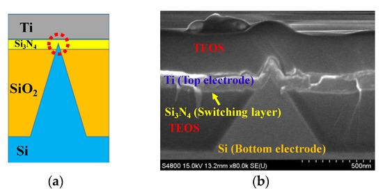
Figure 1.
Cross section of the nano-wedge resistive switching random-access memory (ReRAM) (a) and a SEM image of the fabricated nano-wedge ReRAM (b) A p-type dopant was implanted into the Si bottom electrode, and the Si3N4 is only 5 nm thick, so it is not visible in the taken image.
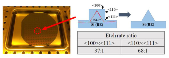
Figure 2.
The anisotropic wet-etching process (left) and formation of the wedge structure from the fin depending on the direction of Si (right).
3. Results and Discussion
All electrical characteristics were obtained in DC mode to examine the multilevel switching characteristics of the fabricated wedge ReRAM. The compliance currents used were 100 μA/200 μA/400 μA/600 μA. The bipolar DC characteristics of the memory device with four different compliance currents are shown in Figure 3.
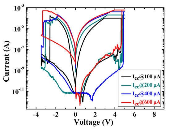
Figure 3.
Bipolar DC characteristics of the fabricated wedge ReRAM under compliance current (Icc) in the range from 100 μA to 600 μA.
At the initial state, voltage was applied to form the conductive filament within the switching layer of the device. At 4.5 V, SET switching occurred as the current level abruptly increased to the limit of the compliance current (Icc) at 100 μA. The actual current may flow more than the compliance current, but it inhibits the maximum current level flowing through the wedge ReRAM. Correspondingly, the RESET voltage was applied to rupture the filament to transform it to a high-resistance state (HRS), which was proved by abrupt dropping of the current level at −2.6 V and −3.3 V with Icc values of 100 μA and 600 μA, respectively.
In Figure 4a, an R–V curve of the RESET process is shown. It is noted that the resistances and currents during the RESET process are shown as absolute values. As the negative voltage increased, there were moments of abrupt resistance change under the four different Icc. It can be seen that the levels of LRS increased as the compliance currents decreased. This indicates that less current flows through the nano-wedge ReRAM as the level of Icc decreases, leading to suppressed LRS. This results in effective control of OFF currents (after transition to the HRS), as seen from Figure 4b. The current levels in Figure 4b are different depending on different Icc. Furthermore, under a compliance current of 100 μA, the current level is clearly differentiated from the rest of the Icc, showing more suppressed LRS under this Icc.
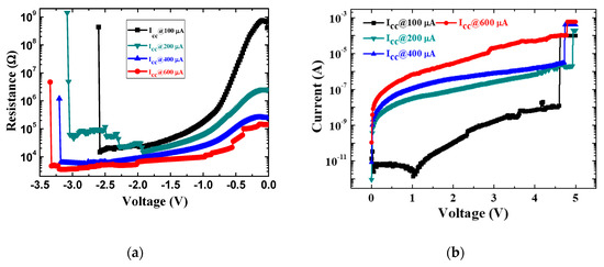
Figure 4.
(a) Resistance–voltage (R–V) curves of the wedge ReRAM device during the RESET process and (b) I–V curves of read currents after transition to the high-resistance state (HRS) under four different compliance currents (Icc).
The reset switching process in ReRAM is known to be associated with Joule heating [13,14]. The flow of current causes a reduction of oxygen vacancies within the switching layer, resulting in rupture of the conductive filament [15]. In order to investigate the effect of the compliance current on reset switching characteristics, the distribution of reset voltages and currents for 50 nano-wedge ReRAM cells was characterized as shown in Figure 5. As can be seen from Figure 5a, the average reset voltages tend to increase as the compliance current increases. This implies a thicker conductive filament where the number of electrons flowing also rises. As a result, higher voltages are required to rupture the number of defects that contribute to current flows. As the radius of the conductive filament becomes wider, the reset current that functions to dismantle the filament also increases, as demonstrated in Figure 5b.
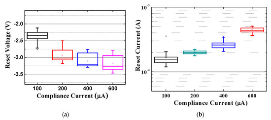
Figure 5.
Effect of compliance current on (a) reset voltages and (b) reset current when reset switching occurs.
Next, the effect of line resistance and array size on current summation was analyzed using SPICE simulation. The purpose of this simulation is important for applications in hardware-implemented neural network processing that require a minimized error rate to maximize the recognition accuracy [16]. In this simulation, array sizes of 8 × 8 and 16 × 16 were used. Table 1 lists the parameters used in the SPICE simulation. RInter-node, BE and RTE represent the resistance of the bottom and top electrodes. Since the resistance of the silicon bottom electrode may vary depending on the size of the cross-point array, unit resistance defined as the inter-node resistance was used as described in Figure 6. The resistance RTE was 42 Ω, which is the commonly known resistance of titanium [17]. In order to measure the current of ReRAM cells, the load resistance was added at the end of the bit line with resistance 100 Ω. Low and high resistances were set as 300 kΩ and 3 MΩ, respectively. The cross-point array structure was simulated based on the connection of resistors as shown in Figure 7. After switching the initial state of ReRAM cells into the low-resistive states, as depicted in red color in Figure 7, a read voltage of 0.2 V was applied to read a single cell. The remaining bit/word lines were grounded while reading every single cell in a bit line, preventing the flow of reverse leakage current through nearby array cells. Equation (1) is the equation explaining the definition of current loss: the difference of the summation of individual array cells and the simultaneous word line access. The larger the difference, the larger the resistance of the bit line where larger voltage drop occurred.

Table 1.
Parameters used in SPICE circuit simulation.
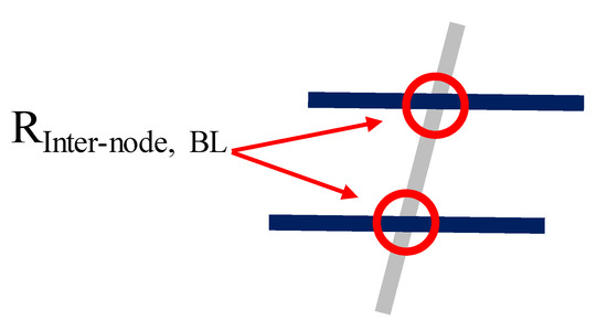
Figure 6.
Inter-node resistance of the bottom electrode (RInter-node, BE) used in the SPICE simulation. This is the unit resistance that could be changed as the array size increases.
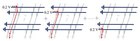
Figure 7.
Schematic of the ReRAM array for read operations. The red dotted line represents the path of current flow after applying a read voltage of 0.2 V. Cells in red color are LRS, while the remaining cells nearby in black colors are HRS. All the reset bit and word lines are grounded except for the target cell.
Equation (1). Definition of current loss: difference between the summation of individual ReRAM cell and simultaneous reads.
After reading every ReRAM cell in the array, an I–V curve reading up to 0.2 V was plotted in Figure 8. The range of the read current from the 8 × 8 array in Figure 8a is from 1.1 µA to 3 µA. The current difference from Figure 9a is attributed to the location of array cells with respect to the ground of the bit line. Due to the existence of bit line resistance, the voltage drop in the bit line becomes larger as the array cell is located farther away from the ground. Figure 8b represents the read current of simultaneous access to the array. Due to the existence of line resistance in the bit line, the simulated current is only 5.55 µA, which is a loss of 62.3% from the summation of individual currents (14.7 µA) in Figure 8a. The results of individual and simultaneous access to the 16 × 16 array cell are shown in Figure 8c,d. Similar to the previous case, the current simulated by simultaneous word line access is 4.2 µA, with the current loss reaching up to 80.7% compared to the summation of individual ReRAM cells (21.9 µA) in the 16 × 16 array. The magnitude of the current loss becomes larger as the array size increases, meaning larger voltage drops in the bit line, causing the loss of ReRAM cell current at the output node.
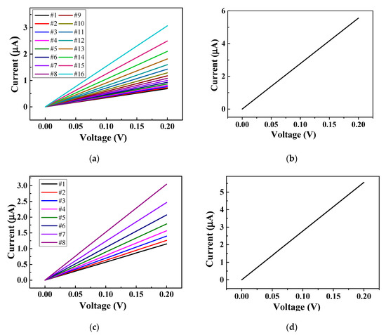
Figure 8.
Simulated I–V curves for read operations of 8 × 8 and 16 × 16 arrays: read currents of individual cells in a single bit line (a) and simultaneous read of the single bit line (b) of a 16 × 16 array; individual (c) and simultaneous (d) reads of an 8 × 8 array.
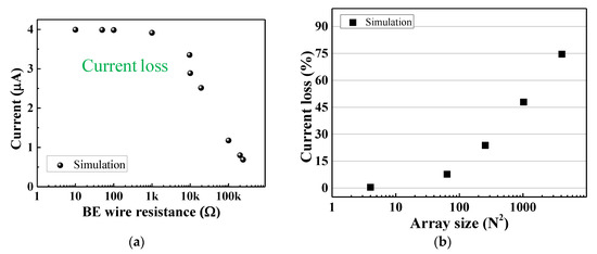
Figure 9.
Simulation of array cell current with respect to bit line (BL) resistance (a) and current loss with respect to array size (b).
For an in-depth analysis of the effect of bit line (BL) resistance on the read current of individual array cells, a simulation was carried out to demonstrate the loss of cell current, as depicted in Figure 9. In Figure 9a, the simulated current value ranges from 3.91 µA to 3.99 µA for bit line resistance ranging from 10 Ω to 1 kΩ. However, the current drops to 2.89 µA as the resistance rises to 10 kΩ. At bit line (BL) resistance of 240 kΩ, the simulated current of the ReRAM array cell is only 689 nA, which is approximately an 82.7% loss compared to the current of BL resistance within the range of 10 Ω–1 kΩ. These results indicate that the effect of BL resistance on the current flow of ReRAM array cells is significant, especially when the resistance increases. Current loss becomes more critical as the array size expands from 2 × 2 to 64 × 64, as illustrated in Figure 9b. For the array size of 2 × 2, the current loss is only 0.43%, while the loss rises to 74.61% as the array size increases to 64 × 64. This aggravation effect is mainly attributed to the larger array having greater resistance in its bit lines, where larger voltage drops occur. Through circuit simulation, it is essential to reduce the line resistance in both bit and word lines to accurately measure the array cell current, which is critical to determining the accuracy of neural networks [18].
4. Conclusions
In this paper, we investigated the switching properties of a Si3N4-based nano-wedge ReRAM device and simulation results for large-sized cross-point arrays. The formation of the wedge structure using TMAH anisotropic wet-etching solution and the effect of variation of the compliance current on the current level were demonstrated. Furthermore, SPICE simulation was carried out to determine the effect of line resistance and array size on the current loss, which is a critical parameter to maximize the accuracy of in-memory computing of neural networks. This research showed that the requirement of a successful neural network depends on minimizing the effect of line resistance, even when the array size increases.
Author Contributions
Investigation, S.K., S.C., M.-H.K., S.B., T.-H.K. and D.K.L.; Supervision, B.-G.P.; Writing—original draft, D.K.L. All authors have read and agreed to the published version of the manuscript.
Funding
This work was supported by the National Research Foundation of Korea (NRF) grant funded by the Ministry of Science, ICT & Future Planning (2018R1A2A1A05023517) and also supported in part by the Brain Korea 21 Plus Program in 2020.
Conflicts of Interest
The authors declare no conflict of interest.
References
- Yu, S.; Wu, Y.; Jeyasingh, R.; Kuzum, D.; Wong, H.-S. An electronic synapse device based on metal oxide resistive switching memory for neuromorphic computation. IEEE Trans. Electr. Devices 2011, 58, 2729–2737. [Google Scholar] [CrossRef]
- Sato, Y.; Tsunoda, K.; Kinoshita, K.; Noshiro, H.; Aoki, M.; Sugiyama, Y. Sub-100-µA reset current of Nickel oxide resistive memory through control of Filamentary conductance by current limit of MOSFET. IEEE Trans. Electr. Devices 2008, 55, 1185–1191. [Google Scholar] [CrossRef]
- Chen, A. A review of emerging non-volatile memory (NVM) technologies and applications. Solid State Electron. 2016, 125, 25–38. [Google Scholar] [CrossRef]
- Wang, W.; Fujita, S.; Wong, S. RESET mechanism of TiOx resistance-change memory device. IEEE Electr. Device Lett. 2009, 30, 733–735. [Google Scholar] [CrossRef]
- Song, S.; Cho, B.; Kim, T.W.; Ji, Y.; Jo, M.; Wang, G.; Choe, M.; Kahng, Y.H.; Hwang, H.; Lee, T. Three-dimensional integration of organic resistive memory devices. Adv. Mater. 2010, 22, 5048–5052. [Google Scholar] [CrossRef] [PubMed]
- Huang, R.; Yan, X.; Ye, S.; Kashtiban, R.; Beanland, R.; Morgan, K.A.; Charlton, M.D.B.; De Groot, C.H. Compliance-free ZrO2/ZrO2 − x/ZrO2 resistive memory with controllable interfacial multistate switching behavior. Nanosc. Res. Lett. 2017, 12, 384. [Google Scholar] [CrossRef] [PubMed]
- Parreira, P.; Paterson, G.W.; McVitie, S.; MacLaren, D.A. Stability, bistability and instability of amorphous ZrO2 resistive memory devices. J. Phys. D Appl. Phys. 2016, 49, 095111. [Google Scholar] [CrossRef]
- Kim, Y.-B.; Lee, S.R.; Lee, D.; Lee, C.B.; Chang, M.; Hur, J.H.; Lee, M.-J.; Park, G.-S.; Kim, C.J.; Chung, U.-I.; et al. Bi-layered RRAM with unlimited endurance and extremely switching. In Proceedings of the 2011 Symposium on VLSI Technology—Digest of Technical Papers, Honolulu, HI, USA, 14–16 June 2011; pp. 52–53. [Google Scholar]
- Kim, K.M.; Jeong, D.S.; Hwang, C.S. Nanofilamentary resistive switching in binary oxide system; A review on the present status and outlook. Nanotechnology 2011, 22, 254002. [Google Scholar] [CrossRef] [PubMed]
- Verbakel, F.; Meskers, S.C.J.; De Leeuw, D.M.; Janssen, R.A.J. Resistive switching in organic memories with a spin-coated metal oxide nanoparticle layer. J. Phys. Chem. C Lett. 2008, 112, 5254–5257. [Google Scholar] [CrossRef]
- Suri, M.; Bichler, O.; Querlioz, D.; Cueto, O.; Perniola, L.; Sousa, V.; Vuillaume, D.; Gamrat, C.; DeSalvo, B. Phase change memory as synapse for ultra-dense neuromorphic systems: Application to complex visual pattern extraction. In Proceedings of the IEEE International Electron Devices Meeting (IEDM), Washington, DC, USA, 5–7 December 2011; pp. 79–82. [Google Scholar]
- Lim, S.; Sung, C.; Kim, H.; Kim, T.; Song, J.; Kim, J.-J.; Hwang, H. Improved synapse device with MLC and conductance linearity using quantized conduction for neuromorphic systems. IEEE Electr. Device Lett. 2018, 39, 312. [Google Scholar] [CrossRef]
- Yu, S.; Wong, H.-S. A phenomenological model for the reset mechanism of metal oxide RRAM. IEEE Electr. Device Lett. 2010, 31, 1455–1457. [Google Scholar] [CrossRef]
- Russo, U.; Ielmini, D.; Cagli, C.; Lacaita, A. Filament conduction and reset mechanism in NiO-based resistive-switching memory (RRAM) devices. IEEE Trans. Electr. Devices 2009, 56, 186–192. [Google Scholar] [CrossRef]
- Ielmini, D. Modeling the universal set/reset characteristics of bipolar RRAM by field-and temperature-driven filament growth. IEEE Trans. Electr. Devices 2011, 58, 4309–4317. [Google Scholar] [CrossRef]
- Chen, Z.; Gao, B.; Zhou, Z.; Huang, P.; Li, H.; Ma, W.; Zhu, D.; Liu, L.; Liu, X.; Kang, J.; et al. Optimized learning scheme for grayscale image recognition in a RRAM based analog neuromorphic system. In Proceedings of the IEEE International Electron Devices Meeting (IEDM), Washington, DC, USA, 7–9 December 2016; pp. 71–84. [Google Scholar]
- Murarka, S.P.; Fraser, D.B.; Sinha, A.K.; Levinstein, H.J. Refractory silicides of titanium and tantalum for low-resistivity gates and interconnects. IEEE J. Solid State Circuits 1980, 15, 474–482. [Google Scholar] [CrossRef]
- Xiang, Y. Impacts of state instability and retention failure of filamentary analog RRAM on the performance of deep neural network. IEEE Trans. Electr. Devices 2019, 66, 4517–4522. [Google Scholar] [CrossRef]


© 2020 by the authors. Licensee MDPI, Basel, Switzerland. This article is an open access article distributed under the terms and conditions of the Creative Commons Attribution (CC BY) license (http://creativecommons.org/licenses/by/4.0/).