A Sub-THz Wireless Power Transfer for Non-Contact Wafer-Level Testing


Abstract
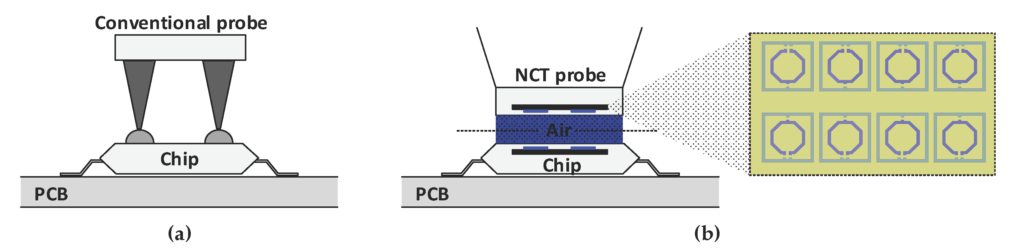
1. Introduction
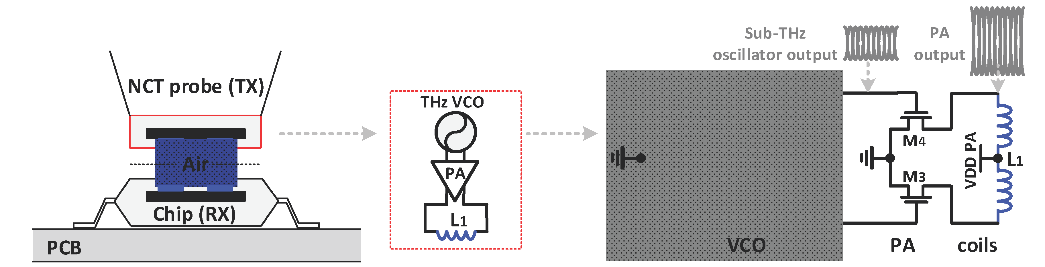
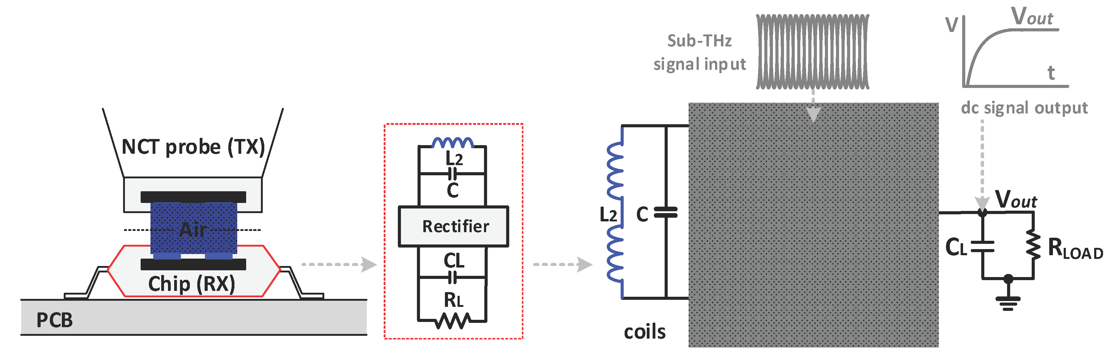
2. The Proposed Sub-THz WPT Design
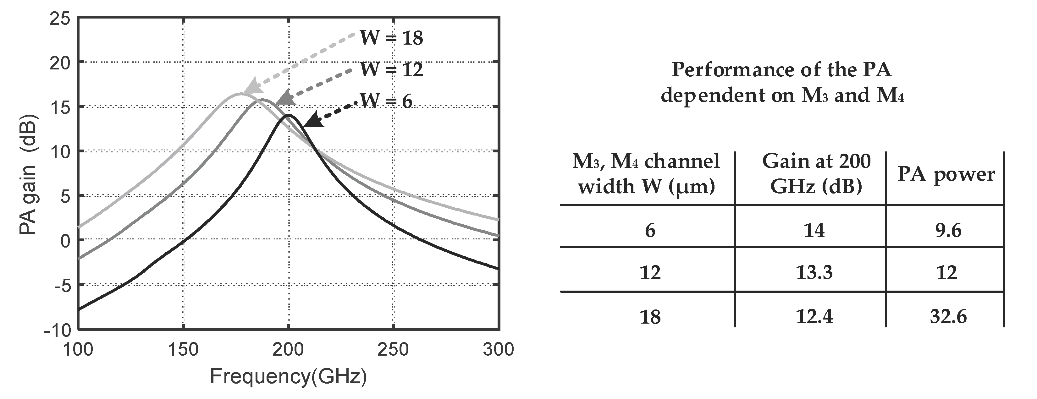
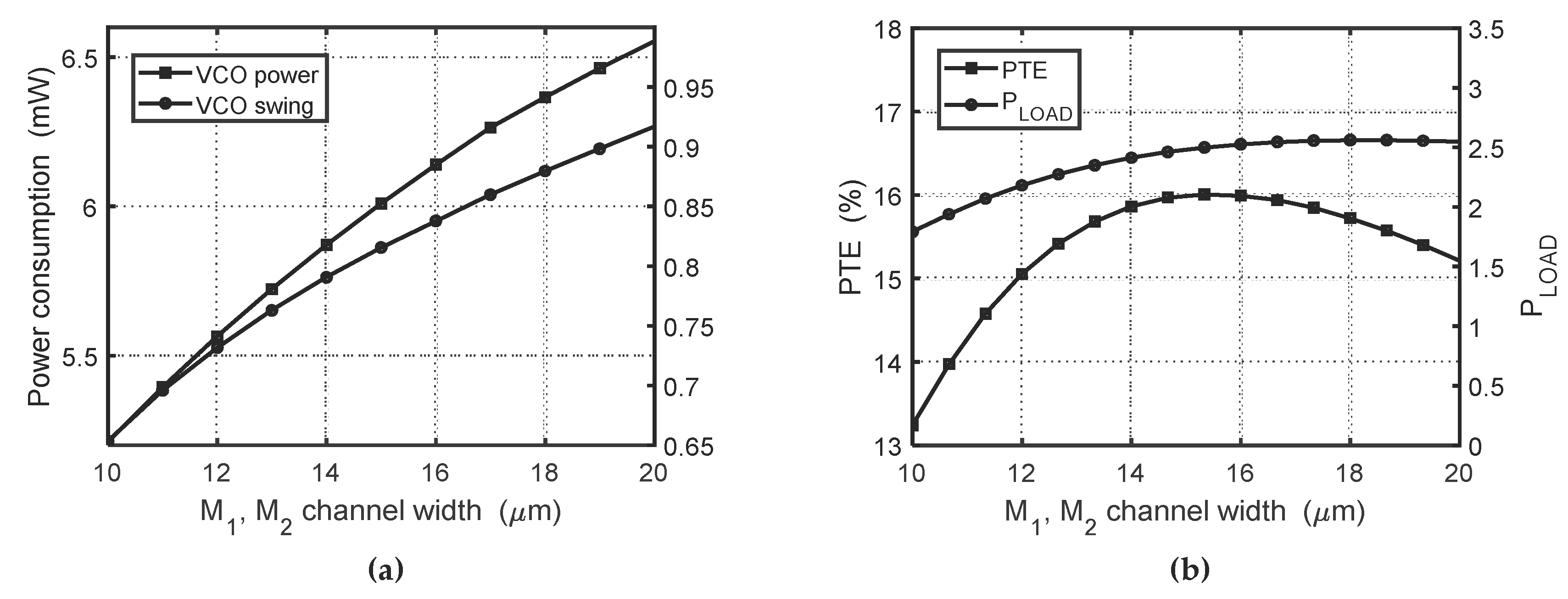
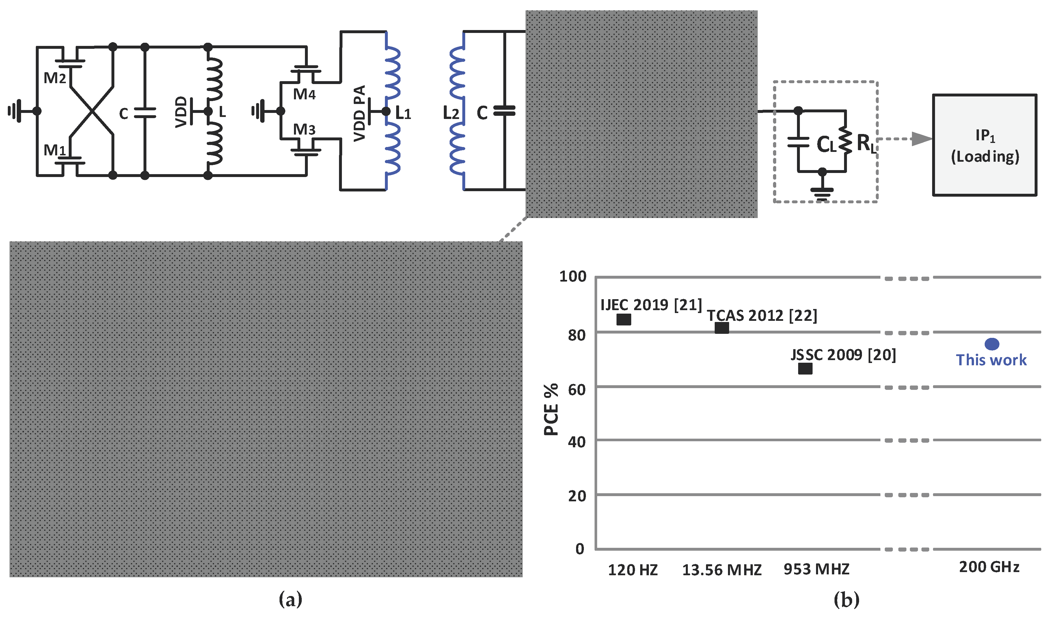
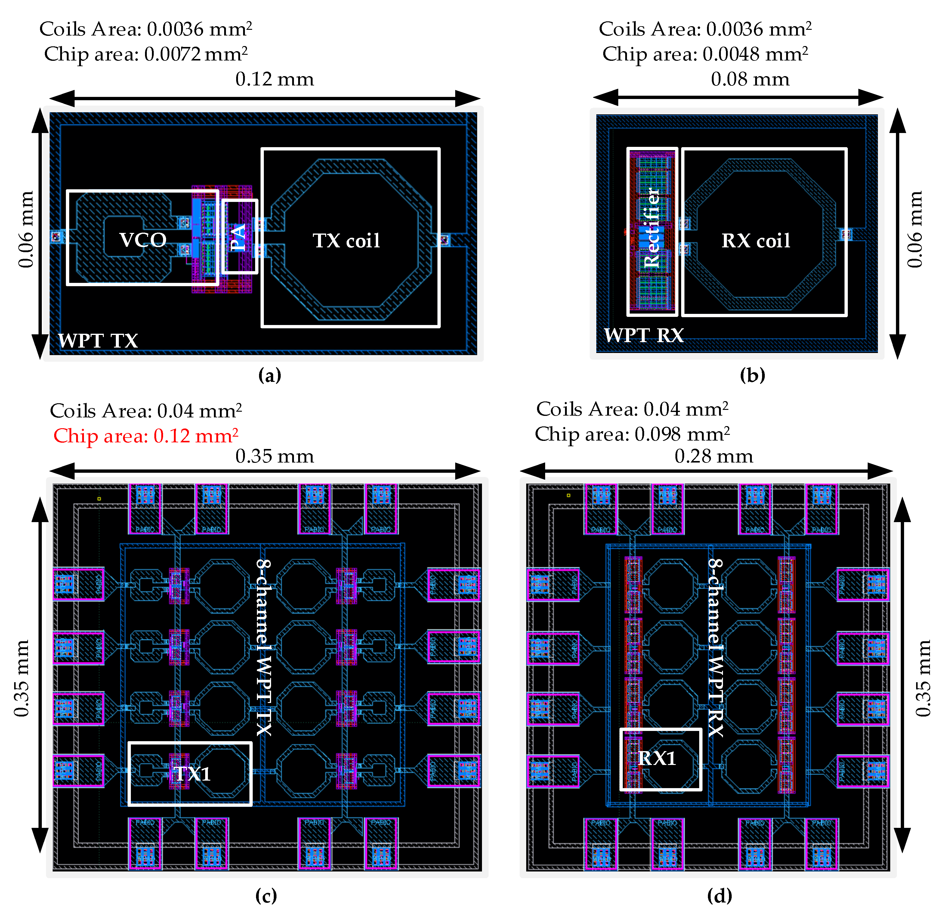
2.1. The Proposed Sub-THz Transmitter Design
2.2. The Proposed Sub-THz Receiver Design
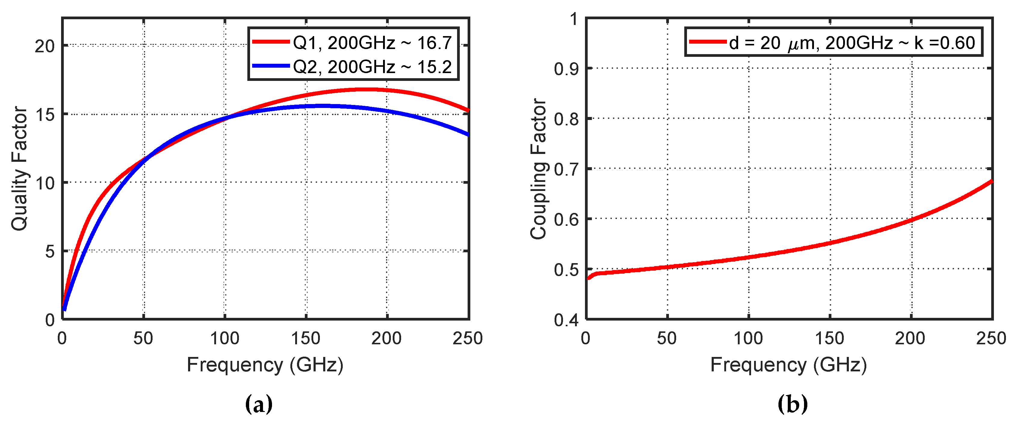
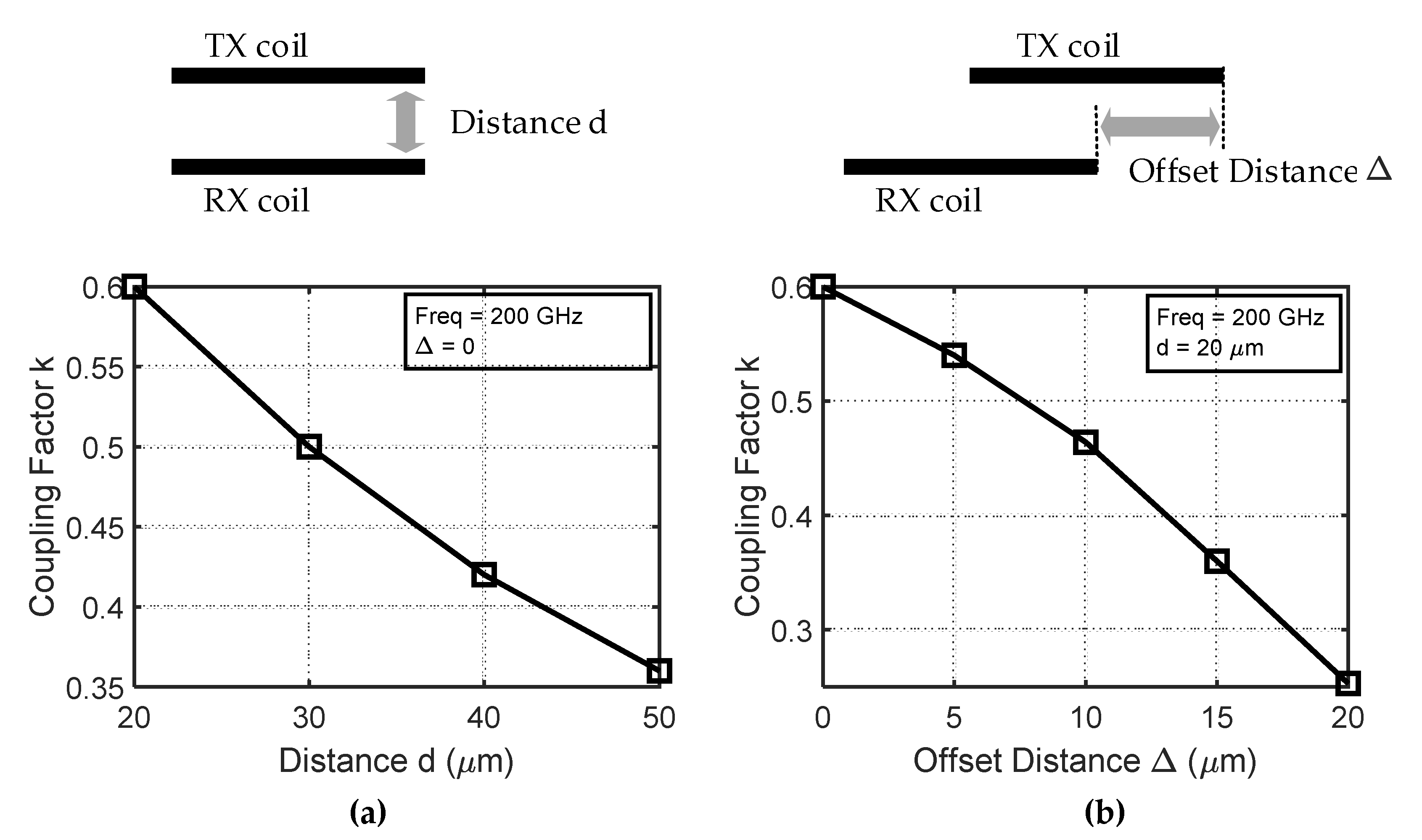
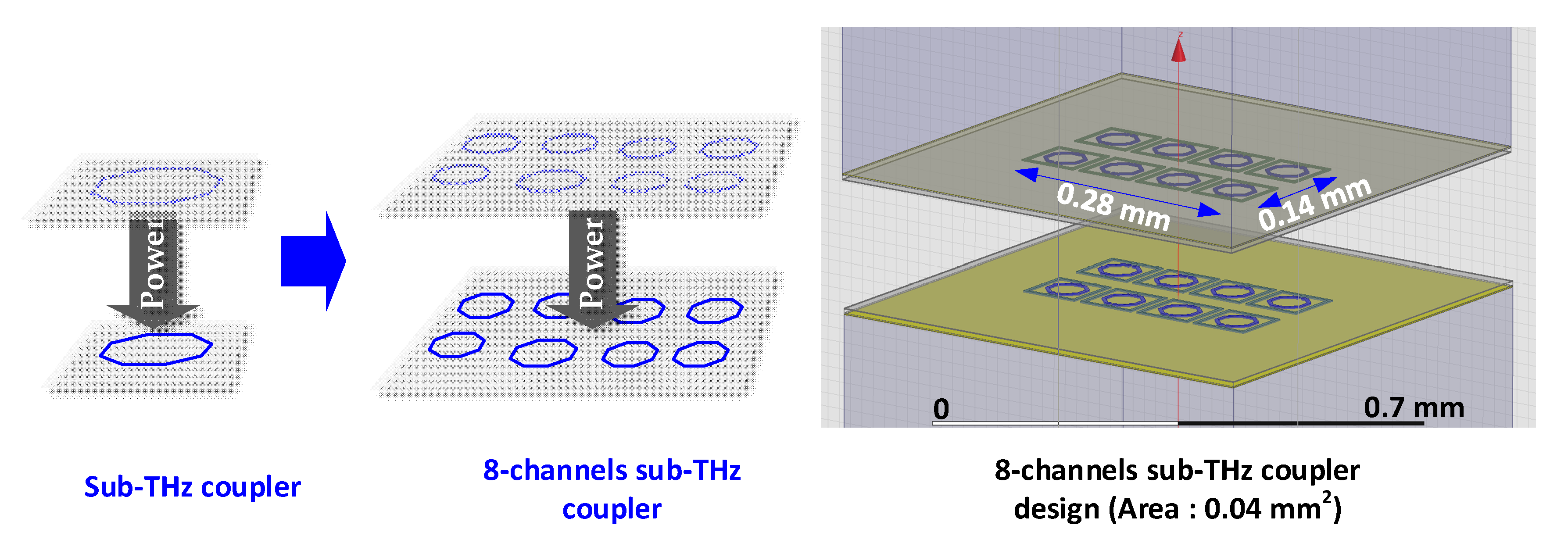
2.3. The Proposed Sub-THz Coupling Coils Design
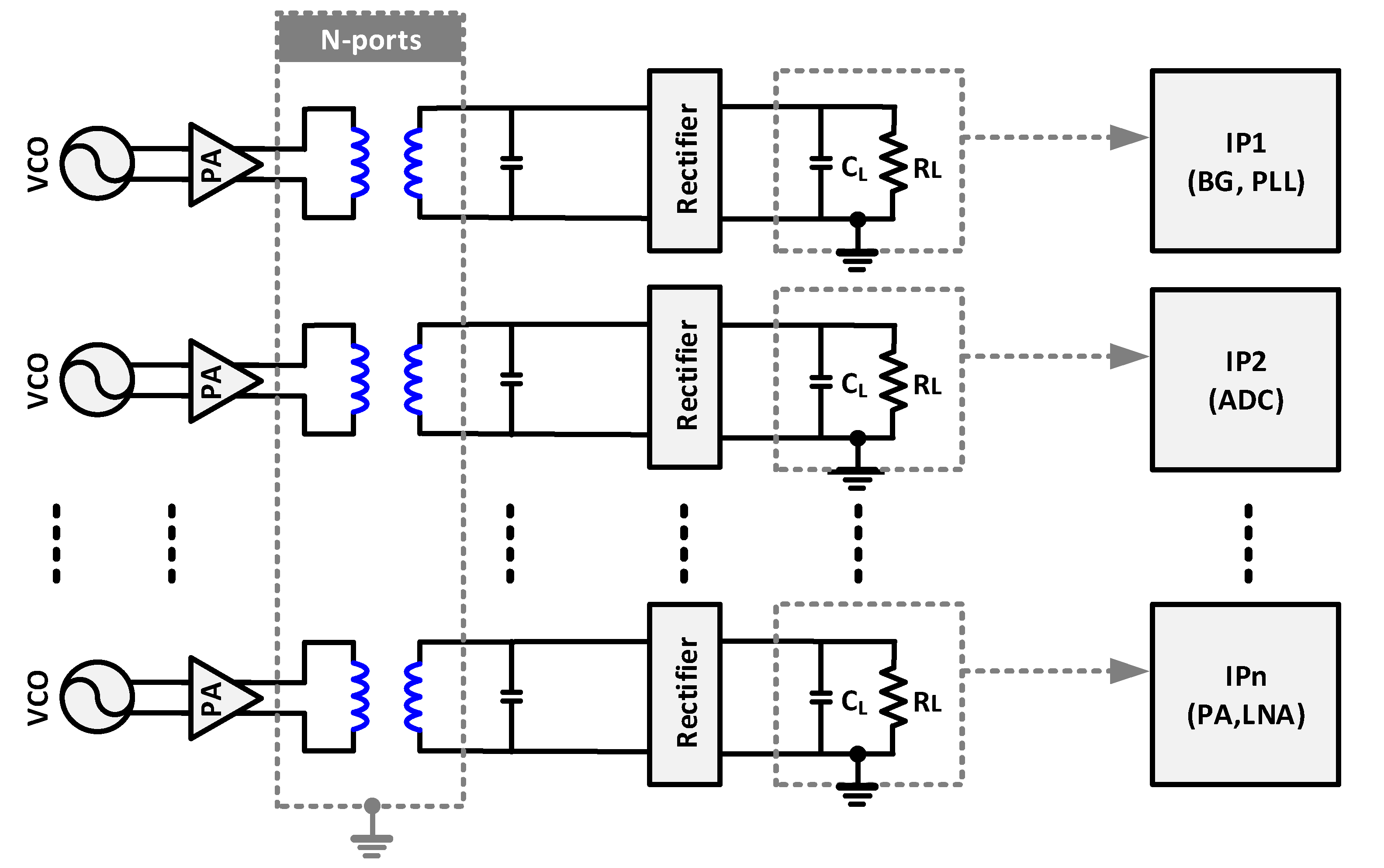
2.4. The Proposed Sub-THz WPT Layout
3. Results
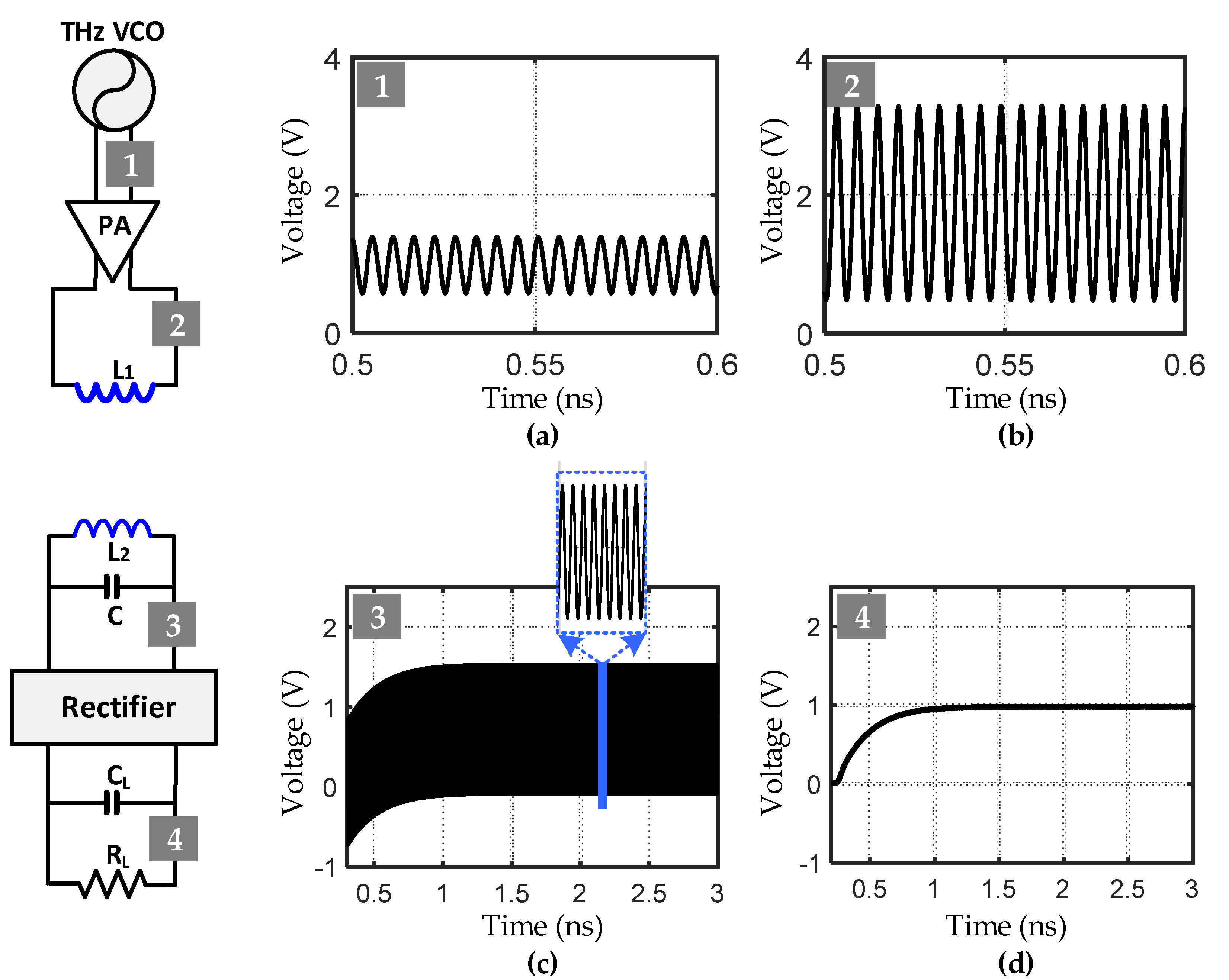
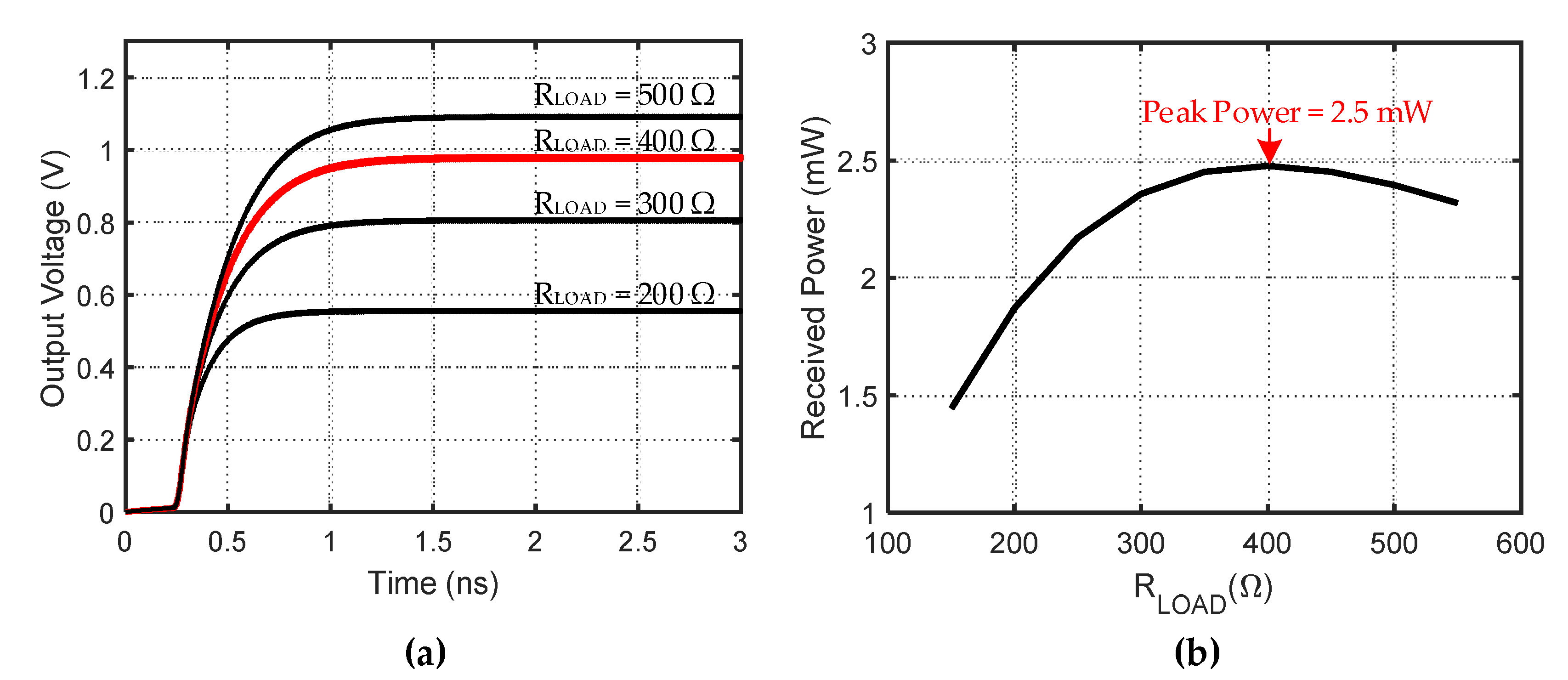
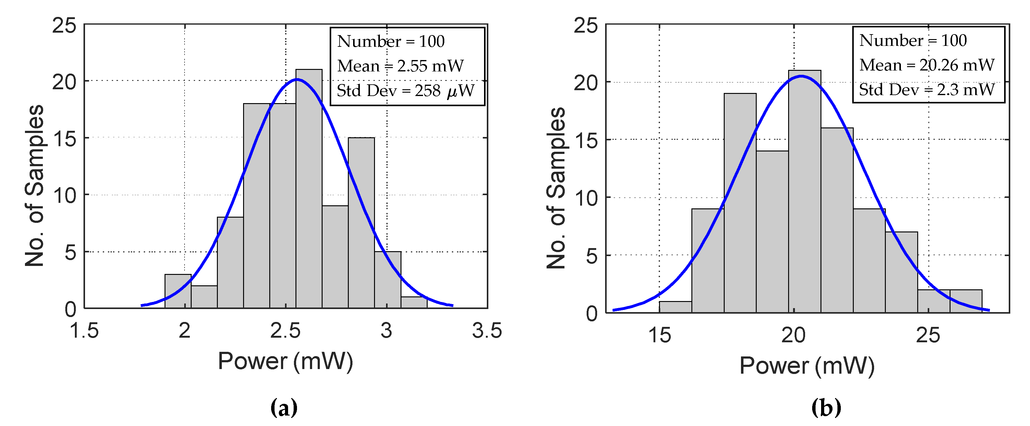
3.1. Simulation Results of a Single Channel Sub-THz WPT Interface
3.2. Simulation Results of a Multi-Channel Sub-THz WPT Interface
4. Conclusions
Author Contributions
Funding
Acknowledgments
Conflicts of Interest
References
- Radecki, A.; Chung, H.; Yoshida, Y.; Miura, N.; Shidei, T.; Ishikuro, H.; Kuroda, T. 6W/25mm 2 inductive power transfer for non-contact wafer-level testing. In Proceedings of the 2011 IEEE International Solid-State Circuits Conference, San Francisco, CA, USA, 20–24 February 2011. [Google Scholar] [CrossRef]
- Lee, M.; Lee, C.; Park, C. Transceiver for wireless power transfer using a cross-coupled oscillator for a wireless on-wafer test. IEEE Trans. Instrum. Meas. 2017, 66, 2097–2105. [Google Scholar] [CrossRef]
- Sellathamby, C.V.; Reja, M.M.; Fu, L.; Bai, B.; Reid, E.; Slupsky, S.H.; Filanovsky, I.M.; Iniewski, K. Noncontact wafer probe using wireless probe cards. In Proceedings of the IEEE International Conference on Test, Charlotte, NC, USA, 6 February 2006; pp. 6–452. [Google Scholar]
- Sasaki, M.; Iwata, A. A 0.95 mW/1.0 Gbps spiral-inductor based wireless chip-interconnect with asynchronous communication scheme. In Proceedings of the Digest of Technical Papers. 2005 Symposium on VLSI Circuits, Kyoto, Japan, 16–18 June 2005; pp. 348–351. [Google Scholar]
- Miura, N.; Kohama, Y.; Sugimori, Y.; Ishikuro, H.; Sakurai, T.; Kuroda, T. An 11Gb/s Inductive-Coupling Link with Burst Transmission. Available online: https://xueshu.baidu.com/usercenter/paper/show?paperid=200853f11db15627204c3fd6a2c6391a&site=xueshu_se (accessed on 17 July 2020).
- Onizuka, K.; Kawaguchi, H.; Takamiya, M.; Kuroda, T.; Sakurai, T. Chip-To-Chip Inductive Wireless Power Transmission System for SiP Applications. Available online: https://www.researchgate.net/publication/224060141_Chip-to-Chip_Inductive_Wireless_Power_Transmission_System_for_SiP_Applications (accessed on 17 July 2020).
- Yuan, Y.; Radecki, A.; Miura, N.; Aikawa, I.; Take, Y.; Ishikuro, H.; Kuroda, T. Simultaneous 6Gb/s data and 10mW power transmission using nested clover coils for non-contact memory card. In Proceedings of the 2010 Symposium on VLSI Circuits, Honolulu, HI, USA, 16–18 June 2010; pp. 199–200. [Google Scholar]
- Kawai, S.; Ishikuro, H.; Kuroda, T. A 2.5 Gb/s/ch 4PAM Inductive-Coupling transceiver for Non-Contact Memory Card. Available online: https://xueshu.baidu.com/usercenter/paper/show?paperid=0595d91182b2c1e235023b4450f5d276&site=xueshu_se (accessed on 17 July 2020).
- Yuxiang, Y.; Miura, N.; Imai, S.; Ochi, H.; Kuroda, T. Digital Rosetta Stone: A Sealed Permanent Memory with Inductive-Coupling Power and Data Link. Available online: https://xueshu.baidu.com/usercenter/paper/show?paperid=5ce9c34bf40c18f4b7e95e485db7afcb&site=xueshu_se (accessed on 17 July 2020).
- Niitsu, K.; Kawai, S.; Miura, N.; Ishikuro, H.; Kuroda, T. A 65 fJ/b inductive-coupling inter-chip transceiver using charge recycling technique for power-aware 3D system integration. In Proceedings of the 2008 IEEE Asian Solid-State Circuits Conference, Fukuoka, Japan, 5 December 2008; pp. 97–100. [Google Scholar]
- Miura, N.; Kasuga, K.; Saito, M.; Kuroda, T. An 8Tb/s 1pJ/b 0.8 mm 2/Tb/s QDR Inductive-Coupling Interface between 65nm CMOS GPU and 0.1 μm DRAM. Available online: https://www.researchgate.net/publication/238733942_Tbs_QDR_Inductive-Coupling_Interface_Between_65nm_CMOS_GPU_and_01m_DRAM (accessed on 17 July 2020).
- Miura, N.; Shidei, T.; Yuan, Y.; Kawai, S.; Takatsu, K.; Kiyota, Y.; Asano, Y.; Kuroda, T. A 0.55 V 10 fJ/bit inductive-coupling data link and 0.7 V 135 fJ/cycle clock link with dual-coil transmission scheme. IEEE J. Solid-State Circuits 2011, 46, 965–973. [Google Scholar] [CrossRef]
- Ahn, D.; Ghovanloo, M. Optimal design of wireless power transmission links for millimeter-sized biomedical implants. IEEE Trans. Biomed. Circuits Syst. 2015, 10, 125–137. [Google Scholar] [CrossRef] [PubMed]
- Yang, C.L.; Chang, C.K.; Lee, S.Y.; Chang, S.J.; Chiou, L.Y. Efficient four-coil wireless power transfer for deep brain stimulation. IEEE Trans. Microwave Theory Tech. 2017, 65, 2496–2507. [Google Scholar] [CrossRef]
- Kim, C.; Ha, S.; Park, J.; Akinin, A.; Mercier, P.P.; Cauwenberghs, G. A 144-MHz fully integrated resonant regulating rectifier with hybrid pulse modulation for mm-sized implants. IEEE J. Solid-State Circuits 2017, 52, 3043–3055. [Google Scholar] [CrossRef]
- Biswas, D.K.; Tasneem, N.T.; Mahbub, I. Optimization of Miniaturized Wireless Power Transfer System to Maximize Efficiency for Implant Biomedical Devices. Available online: https://www.researchgate.net/publication/332261113_Optimization_of_Miniaturized_Wireless_Power_Transfer_System_to_Maximize_Efficiency_for_Implantable_Biomedical_Devices (accessed on 17 July 2020).
- Shah, S.A.A.; Yoo, H. Radiative Near-Field Wireless Power Transfer to Scalp-Implantable Biotelemetric Device. IEEE Trans. Microwave Theory Tech. 2020, 68, 2944–2953. [Google Scholar] [CrossRef]
- Radecki, A.; Yuan, Y.; Miura, N.; Aikawa, I.; Take, Y.; Ishikuro, H.; Kuroda, T. Simultaneous 6-Gb/s data and 10-mW power transmission using nested clover coils for noncontact memory card. IEEE J. Solid-State Circuits 2012, 47, 2484–2495. [Google Scholar] [CrossRef]
- Finocchiaro, A.; Girlando, G.; Motta, A.; Pagani, A.; Ragonese, E.; Palmisano, G. Wafer-Level Contactless Testing Based on UHF RFID Tags With Post-Process On-Chip Antennas. IEEE Trans. Circuits Syst. Express Briefs 2018, 65, 1355–1359. [Google Scholar] [CrossRef]
- Ghovanloo, M.; Najafi, K. Fully integrated wideband high-current rectifiers for inductively powered devices. IEEE J. Solid-State Circuits 2004, 39, 1976–1984. [Google Scholar] [CrossRef]
- Kotani, K.; Sasaki, A.; Ito, T. High-efficiency differential-drive CMOS rectifier for UHF RFIDs. IEEE J. Solid-State Circuits 2009, 44, 3011–3018. [Google Scholar] [CrossRef]
- Yuen, P.W.; Chong, G.; Ramiah, H. A high efficient dual-output rectifier for piezoelectric energy harvesting. AEU Int. J. Electron. Commun. 2019, 111, 152922. [Google Scholar] [CrossRef]
- Cha, H.-K.; Park, W.-T.; Je, M. A CMOS rectifier with a cross-coupled latched comparator for wireless power transfer in biomedical applications. IEEE Trans. Circuits Syst. Express Briefs 2012, 59, 409–413. [Google Scholar] [CrossRef]
- Hui, S.Y.R.; Zhong, W.; Lee, C.K. A critical review of recent progress in mid-range wireless power transfer. IEEE Trans. Power Electron. 2013, 29, 4500–4511. [Google Scholar] [CrossRef]
- Lu, F.; Zhang, H.; Hofmann, H.; Mi, C.C. An inductive and capacitive combined wireless power transfer system withLC-compensated topology. IEEE Trans. Power Electron. 2016, 31, 8471–8482. [Google Scholar] [CrossRef]
- Narayanamoorthi, R. Modeling of Capacitive Resonant Wireless Power and Data Transfer to Deep Biomedical Implants. IEEE Trans. Compon. Packag. Manuf. Technol. 2019, 9, 1253–1263. [Google Scholar] [CrossRef]
- Yuxiang, Y.; Yoshida, Y.; Kuroda, T. Non-Contact 10% Efficient 36mW Power Delivery Using on-Chip Inductor in 0.18-μm CMOS. Available online: https://xueshu.baidu.com/usercenter/paper/show?paperid=ad93f441519ed74e64469a5c60f7f5d8&site=xueshu_se (accessed on 17 July 2020).
- Miller, J.M.; Onar, O.C.; Chinthavali, M. Primary-side power flow control of wireless power transfer for electric vehicle charging. IEEE J. Emerg. Sel. Top. Power Electron. 2014, 3, 147–162. [Google Scholar] [CrossRef]
- Lu, F.; Zhang, Y.; Zhang, H.; Zhu, C.; Diao, L.; Gong, M.; Zhang, W.; Mi, C. A low-voltage and high-current inductive power transfer system with low harmonics for automatic guided vehicles. IEEE Trans. Veh. Technol. 2019, 68, 3351–3360. [Google Scholar] [CrossRef]
- Halim, M.A.; Smith, S.E.; Samman, J.M.; Arnold, D.P. A High-Performance Electrodynamic Micro-Receiver for Low-Frequency Wireless Power Transfer. Available online: https://xueshu.baidu.com/usercenter/paper/show?paperid=126v0e20x37d0010rd2k0r10b7595652&site=xueshu_se&hitarticle=1 (accessed on 17 July 2020).


| Unit | This Work | JSSC 2012 [18] | TBCS 2016 [13] | TMTT 2017 [14] | JSSC 2017 [15] | TIM 2017 [2] | TCAS 2018 [19] | TSWMCS 2019 [16] | TMTT 2020 [17] | |
|---|---|---|---|---|---|---|---|---|---|---|
| Received Power, PRX | mW | 20 | 10 | 0.224 | 18 | 0.16 | 5.29 | N/A | 79.43 | N/A |
| RX Area, ARX | mm2 | 0.098 | 0.49 | 1 | 25 | 9 | 0.87 | 0.45 | 36 | 33.6 |
| TX Area, ATX | mm2 | 0.12 | 0.49 | 576 | 900 | 625 | 0.93 | N/A | 784 | 2500 |
| Distance, d | mm | 0.02 | 0.02 | 12 | 10 | 10 | 0.1 | 2.5 | 10 | 20 |
| Efficiency, η | % | 16 | 10 | 1.02 | 19.1 | 1.23 | 37.5 | N/A | 21 | 5.1 |
| Carrier Frequency, fc | GHz | 200 | 0.3 | 0.2 | 0.0136 | 0.144 | 0.144 | 0.865 | 0.025 | 1.9 |
| Supply Voltage, VDD | V | 1.0/1.8 * | 1.2 | N/A | 2 | 1.5 | 1.9 | N/A | N/A | N/A |
| CMOS Technology | nm | 28 | 350 | N/A | 180 | 180 | 180 | 180 | 65 | N/A |
© 2020 by the authors. Licensee MDPI, Basel, Switzerland. This article is an open access article distributed under the terms and conditions of the Creative Commons Attribution (CC BY) license (http://creativecommons.org/licenses/by/4.0/).
Share and Cite
Dang-ba, H.; Byun, G.-s. A Sub-THz Wireless Power Transfer for Non-Contact Wafer-Level Testing. Electronics 2020, 9, 1210. https://doi.org/10.3390/electronics9081210
Dang-ba H, Byun G-s. A Sub-THz Wireless Power Transfer for Non-Contact Wafer-Level Testing. Electronics. 2020; 9(8):1210. https://doi.org/10.3390/electronics9081210
Chicago/Turabian StyleDang-ba, Hanh, and Gyung-su Byun. 2020. "A Sub-THz Wireless Power Transfer for Non-Contact Wafer-Level Testing" Electronics 9, no. 8: 1210. https://doi.org/10.3390/electronics9081210
APA StyleDang-ba, H., & Byun, G.-s. (2020). A Sub-THz Wireless Power Transfer for Non-Contact Wafer-Level Testing. Electronics, 9(8), 1210. https://doi.org/10.3390/electronics9081210