Article

Interleaved Buck Converter for Inductive Wireless Power Transfer in DC–DC Converters

by
Marco Carbajal-Retana
,
Leobardo Hernandez-Gonzalez
*,
Jazmin Ramirez-Hernandez
,
Juan Gerardo Avalos-Ochoa
*,
Pedro Guevara-Lopez
,
Igor Loboda
and
Luis Antonio Sotres-Jara
Escuela Superior de Ingeniería Mecánica y Eléctrica, Unidad Culhuacan, Instituto Politécnico Nacional, Av. Santa Ana No. 1000, Mexico 04430, Mexico
*
Authors to whom correspondence should be addressed.
Electronics 2020, 9(6), 949; https://doi.org/10.3390/electronics9060949
Submission received: 12 May 2020 / Revised: 2 June 2020 / Accepted: 5 June 2020 / Published: 8 June 2020
(This article belongs to the Special Issue Design and Applications of Multiple Output DC-DC Converters)

Abstract

:
The use of Inductive Wireless Power Transfer (IWPT) varies from low-power applications such as mobile phones and tablets chargers to high-power electric vehicles chargers. DC–DC converters are used in IWPT systems, and their design needs to consider the demand of high efficiency in the power transfer. In this paper, a DC–DC power converter for IWPT is proposed. Its topology uses a DC–AC converter in the transmitter circuit and an AC–DC converter in the receptor. The transmitter has an interleaved coupled-Buck converter that integrates two Buck converters connected to a half inverter bridge and a parallel resonant load. The control strategy implemented for the semiconductor switching devices allows two operating modes to obtain a sinusoidal output voltage with a low distortion that makes it suitable in high-efficiency power transfer systems. To obtain a DC output voltage, a full wave bridge rectifier is used in the receptor circuit. The proposed topology and the control strategy are validated with simulation and experimental results for a 15 W prototype.

1. Introduction

The increasing use of mobile and electronic devices as basic tools for daily activities has generated the need for novel technologies for battery recharging. The Wireless Power Transfer (WPT) has been considered as an option to make the battery recharging more convenient, safe, and automatic [1,2]. The WPT can be made through an inductive power transfer (IPT) and capacitive power transfer (CPT) [3,4,5]. Since IPT is applicable to many power levels and gap distances, its use has been considered in battery recharge topologies [6,7]; some of them include bidirectional data transfer [8]. Special attention should be paid to the design of intermediate conversion stages to obtain a sinusoidal signal with low distortion to be transferred.
Some proposed topologies imply a sinusoidal signal generated by cascade schemes with a DC–DC converter connected to resonant circuits [9,10]. These topologies are complex and limit the converter efficiency when the design parameters, for example, the gap distance and aligning between coils, change. The topologies also present some additional disadvantages: the use of energy storage elements that increase losses in parasitic elements and reduce the lifetime of the converters [11]; the need to employ complex control strategies for obtaining a specific output level and improving the Total Harmonic Distortion (THD) [12]; too high number of semiconductor devices used in some topologies [13].
The proposed scheme integrates two buck converters connected to a half inverter bridge to generate an AC signal that is processed by a parallel resonant circuit conformed by the output buck capacitor and a transmitter inductor. A burst Pulse Width Modulation (PWM) signal is used to control the semiconductor devices according to the symmetrical operation of the buck converters. The amplitude of the sinusoidal output voltage can be determined by the duty cycle D of its operation. Finally, a full wave bridge rectifier is used to obtain the desired DC output voltage. The proposed topology exhibits the following advantages: first, the generation of a sinusoidal signal with low THD in the DC–AC conversion stage increases the efficiency in the converter; second, a DC–AC proposed topology allows the reduction of switching and conduction losses, and, third, a simple control strategy with two PWM burst complementary signals is used to handle the output voltage level.
Simulation results obtained in Saber Sketch and experimental results for a 15 W prototype are provided in the article, validating the presented principle of operation.

2. Principle of Operation of Proposed Converter

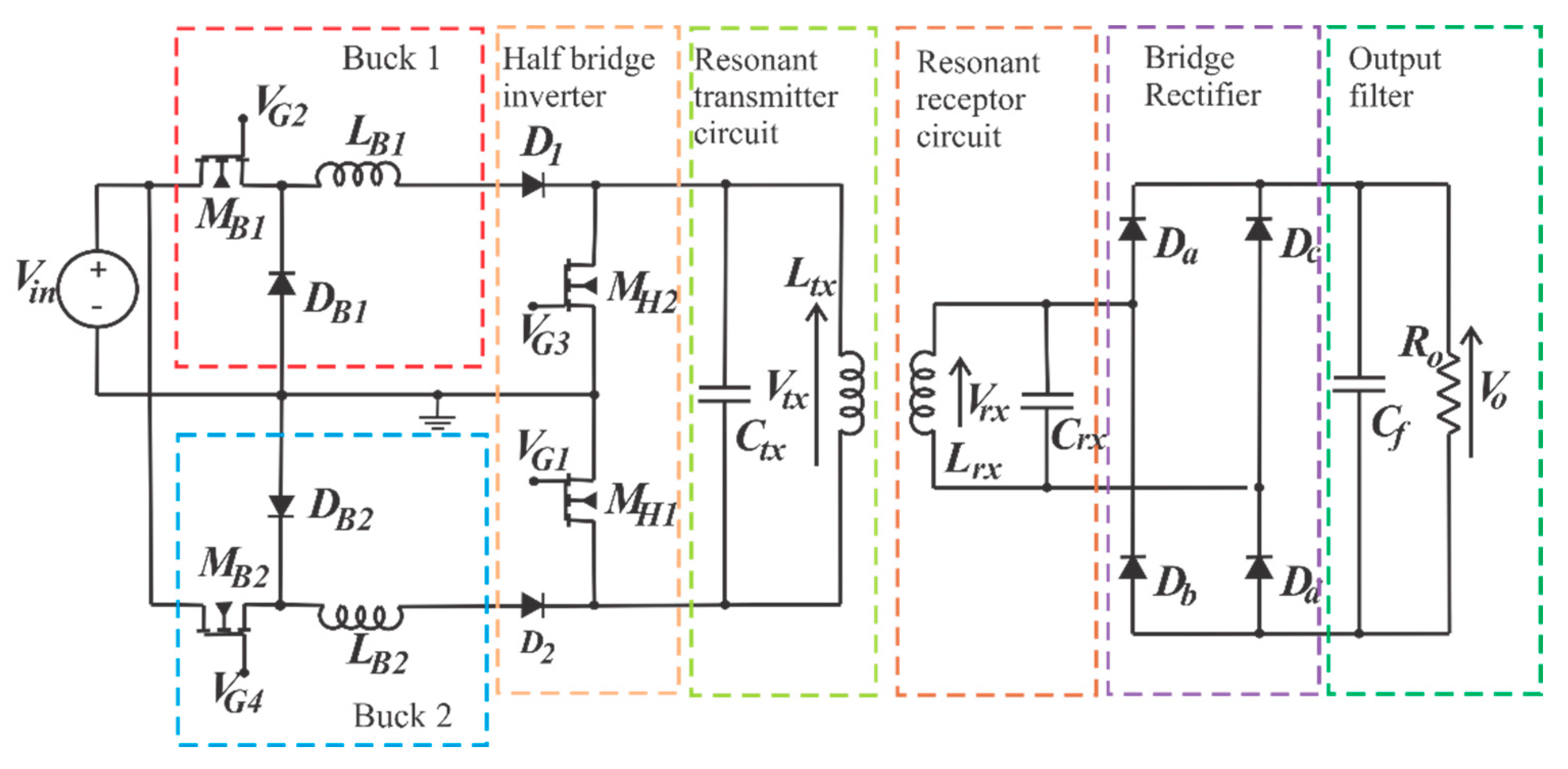
2.1. Circuit Description

The proposed DC–DC converter is shown in Figure 1. The first buck converter is delimited with a red color. Its topology includes the switching device MB1, the inductor LB1, and the diode DB1. The second buck converter, delimited by a blue color, is formed by MB2, LB2, and DB2.
The output of the buck converters is connected to a half bridge inverter conformed by the semiconductor devices MH2 and MH1. To make the converter compact, the capacitor Ctx works as a filter for both buck converters and is also used in the parallel resonant circuit to operate together with the coupled inductor Ltx to obtain a sinusoidal waveform. The receptor has a resonant LC parallel circuit with the coupled inductor Lrx and capacitor Crx; its output is connected to a full wave bridge rectifier (Da, Db, Dc, and Dd) to obtain the DC output voltage.

2.2. Principle of Operation

The principle of operation of the DC–DC converter is based on the generation of two PWM complementary signals, VG1 and VG3, that control the half inverter bridge and two burst PWM signals, VG2 and VG4, that control the operation of the buck converters, as shown in Figure 2.
The synchronization of the four signals generates a square output voltage Vbuck with an amplitude determined by the duty cycle D of the buck converters operation in its continuous mode. During the first half of the time period THB, the top Buck converter generates the positive output voltage +VBuck, and, during the second half of THB, the bottom Buck converter generates the negative voltage −VBuck. The resonant circuit composed from Ctx and Ltx is used to obtain a sinusoidal output voltage with the same amplitude of Vbuck and a peak amplitude Vtxpk defined by Equation (1), where Vin is the input voltage of the converter:
V t x p k = 4 D V i n π
The control signals of Figure 2 generate two operating modes:
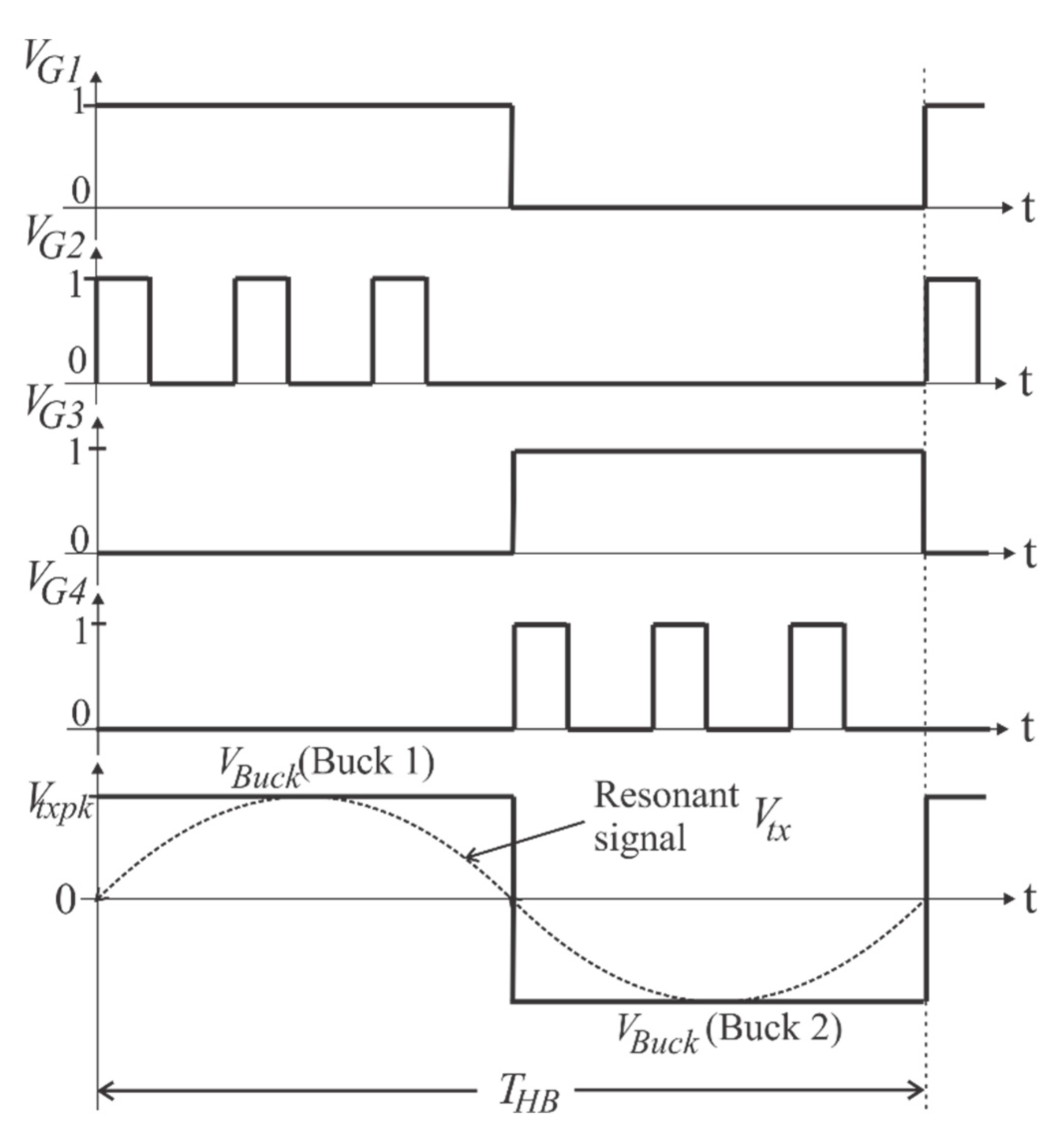
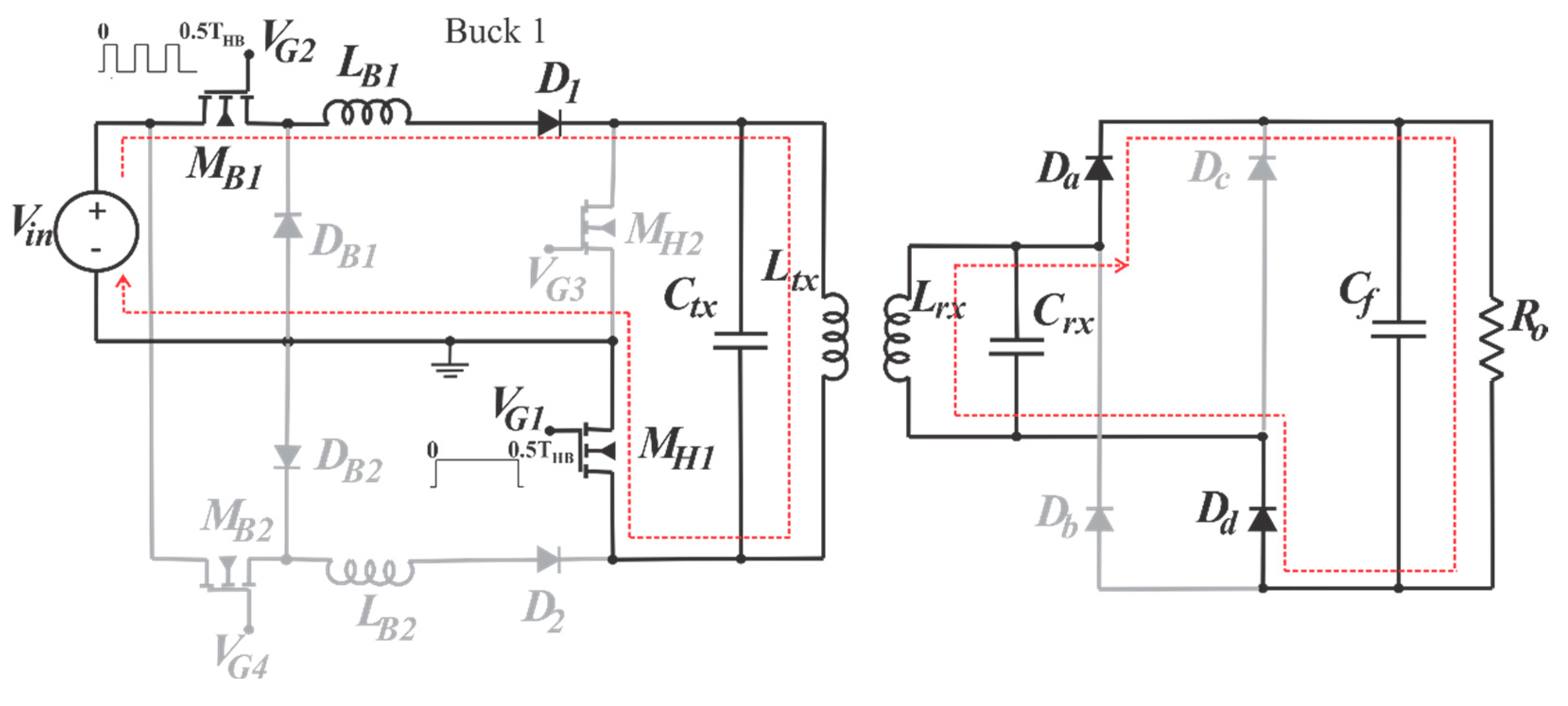
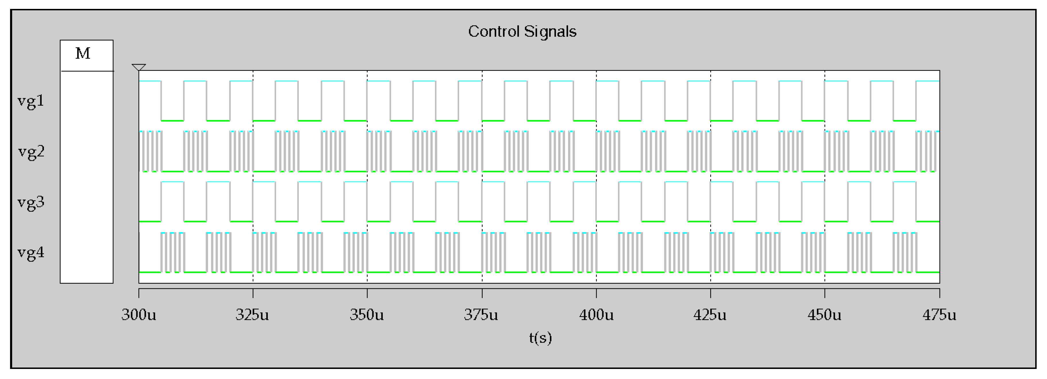
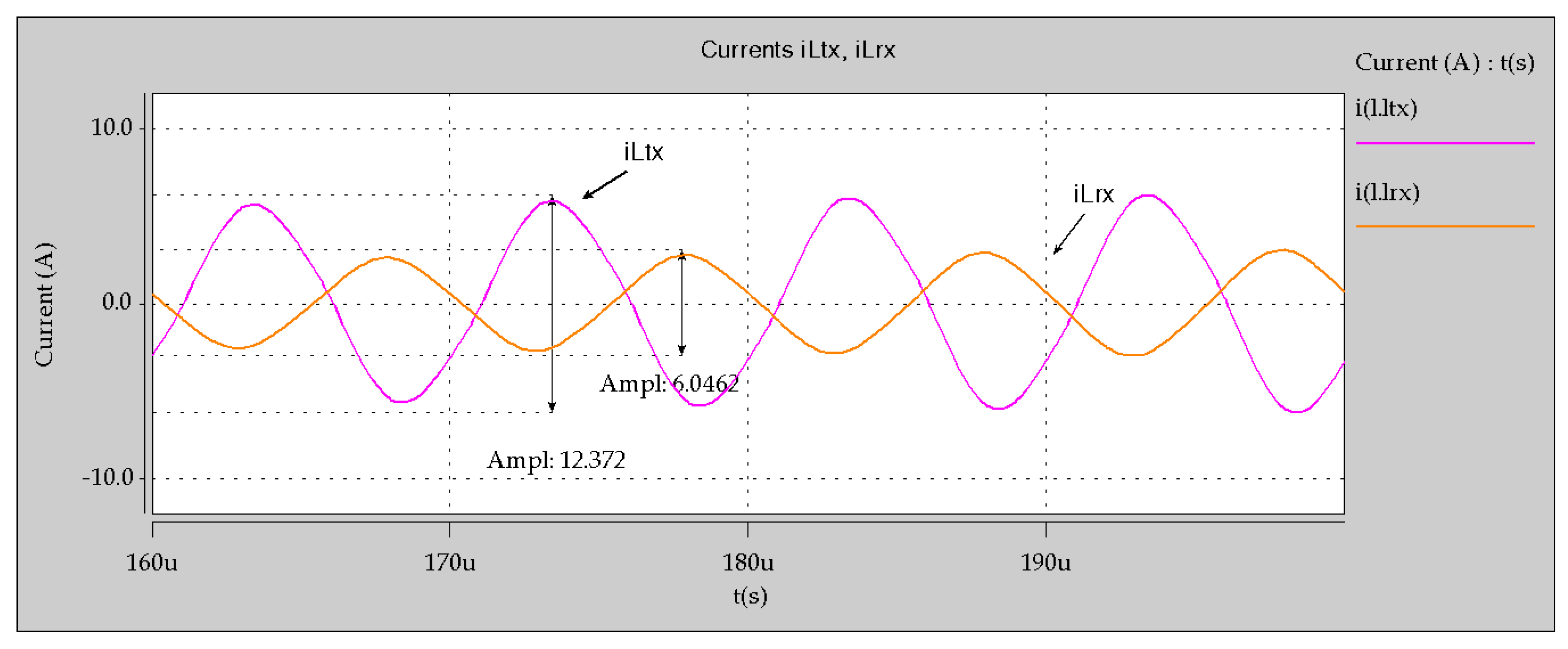
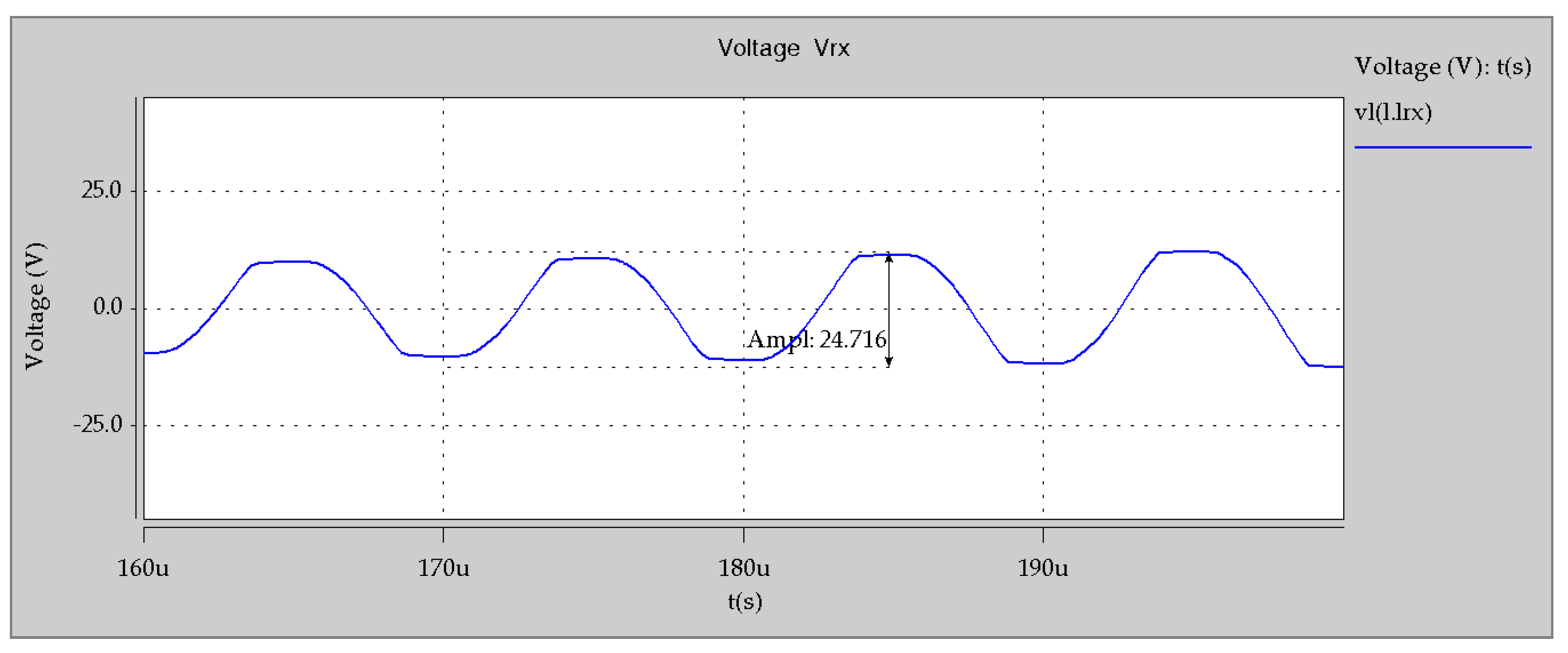
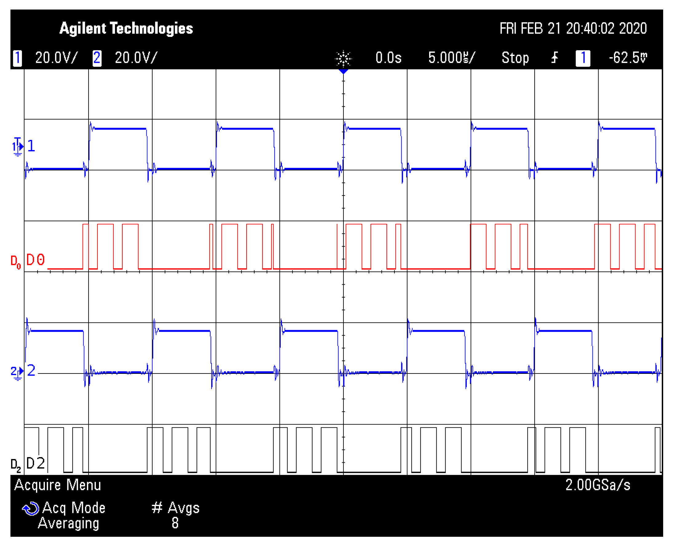
  • Mode I for the interval 0 < t < 0.5 THB. Figure 3 shows the equivalent circuit when MB1 and MH1 are in the on state. The current flows through the resonant load obtaining the positive half cycle of the expected sinusoidal signal. The peak amplitude is determined by the buck converter output voltage VBuck, which is controlled through D of the PWM burst signal. In the rectifier, the diodes Da and Dd are in the on state during the positive half cycle of the voltage vrx.
A state-space representation for the DC–AC conversion in the form X’ = AX + BU may be used to model the circuit operation in Mode I. Considering x1 = iLB1, x2 = iLB2, x3 = vtx and x4 = iLtx as the state variables, the system can be modeled according to Equation (2).
[ i L B 1 i L B 2 V t x i L t x ] = [ 0 0 0 0 0 0 1 L B 2 0 0 1 C t x 0 1 C t x 0 0 1 L t x 0 ] [ i L B 1 i L B 2 V t x i L t x ] + [ 0 1 L B 2 0 0 ] V i n
2.
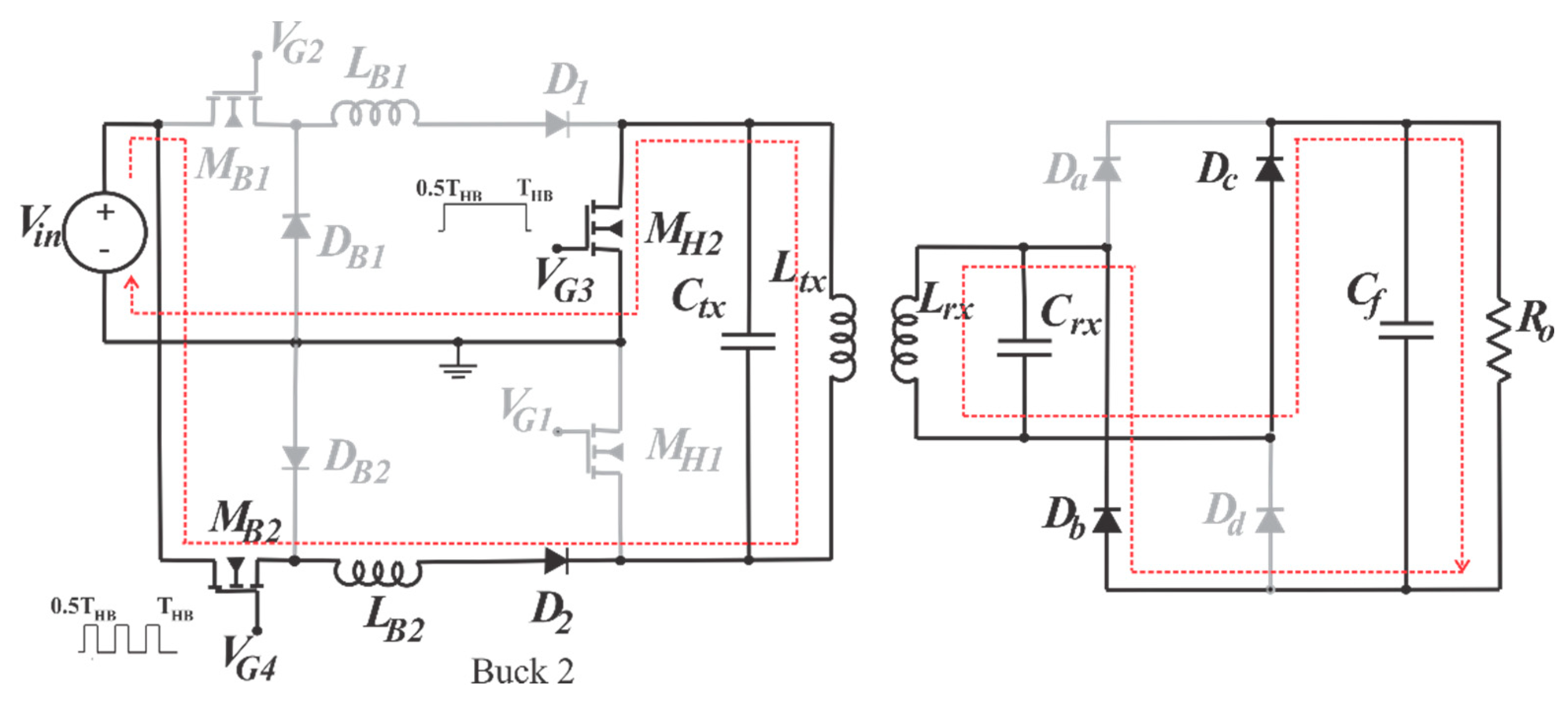
Mode II for the interval 0.5 THB < t < 1 THB. Figure 4 shows the equivalent circuit when MB2 and MH2 are in the on state. The current through the resonant circuit flows in the opposite direction of Mode I to generate the negative half cycle of the sinusoidal signal. The output signal peak amplitude is determined by the voltage VBuck, which is controlled through D of the PWM burst signal. In the rectifier, diodes Db and Dc are in the on state during the negative half cycle of the voltage vrx.
The state-space representation for the DC–AC converter that models the circuit operation of Mode II can be denoted as follows:
[ i L B 1 i L B 2 V t x i L t x ] = [ 0 0 1 L B 1 0 0 0 0 0 1 C t x 0 0 1 C t x 0 0 1 L t x 0 ] [ i L B 1 i L B 2 V t x i L t x ] + [ 1 L B 1 0 0 0 ] V i n .

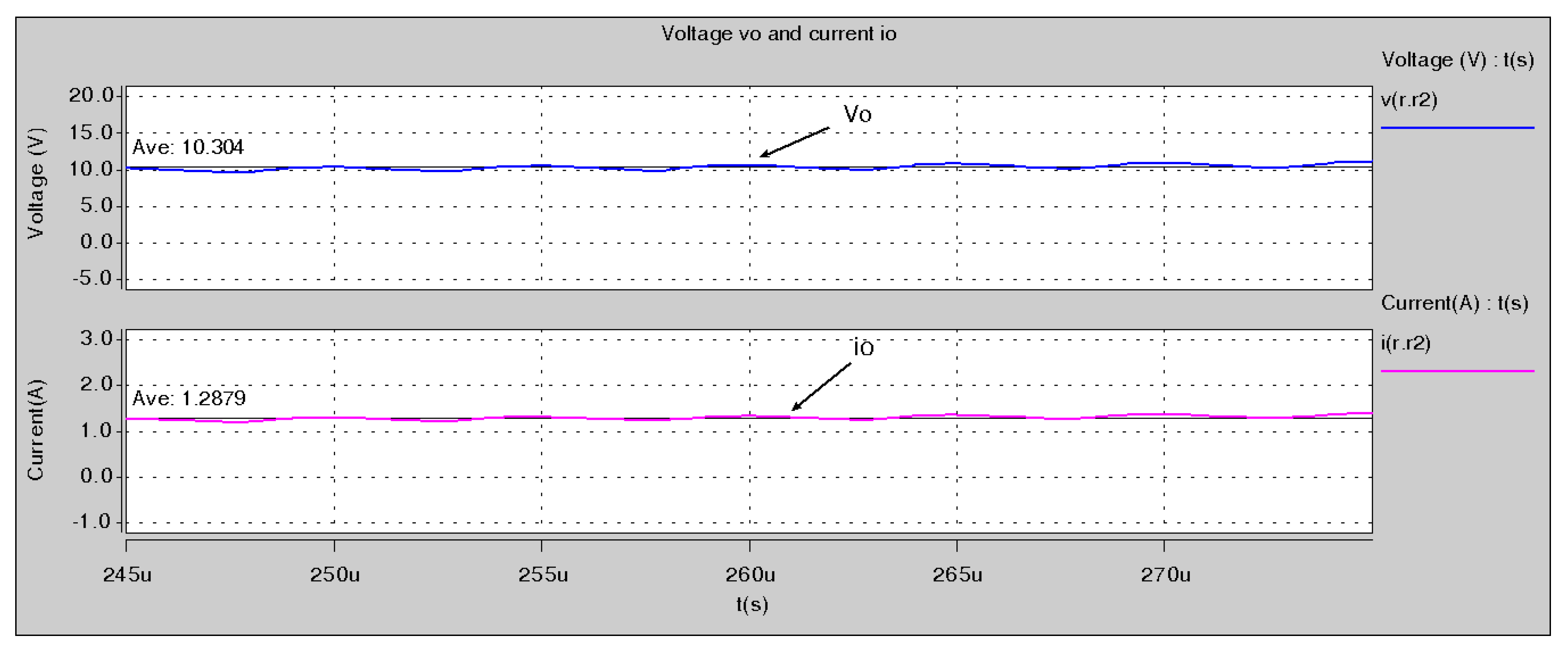
3. Simulation Results

To verify the principle of operation of the proposed DC–DC converter, a simulation in Saber was performed using the variables and calculated component parameters listed in Table 1. The principal components are obtaining according to Equations (4)–(7) [14]. The simulation uses ideal components and does not consider parasitic components.
L B 1 = L B 2 = ( V i n V o ) Δ I o f B u r s t 130 μ H
C t x = 1 ( 2 π F H B ) 2 L t x 0.47 μ F
C r x = 1 ( 2 π F H B ) 2 L r x 220 n F
The control signals VG1, VG2, and VG3, VG4, that are used to activate MB1, MH1, MB2, and MH2 respectively, are shown in Figure 5. The switching frequency of the half bridge, signals VG1 and VG3, is 100 kHz, and the burst signals that commutate the semiconductor devices in the buck converters operate at 500 kHz, with a D = 0.6.
The correct energy transmission through the coupled inductors is verified in Figure 6 and Figure 7. The currents through inductors Ltx and Lrx, iLtx and iLrx, respectively, are shown in Figure 6 using a coupling factor of 0.5; it can be denoted that the peak-to-peak amplitude of iLtx and irtx are 12.32 A and 6.04 A, respectively. Figure 7 shows the voltage in inductor Lrx, vrx, with an amplitude of 24.7 V.
Figure 8 analyzes the voltage and current in the output resistive load Ro, vo, obtaining a DC level (average measure) of Vo = 10.304 V and Io = 1.28 A.

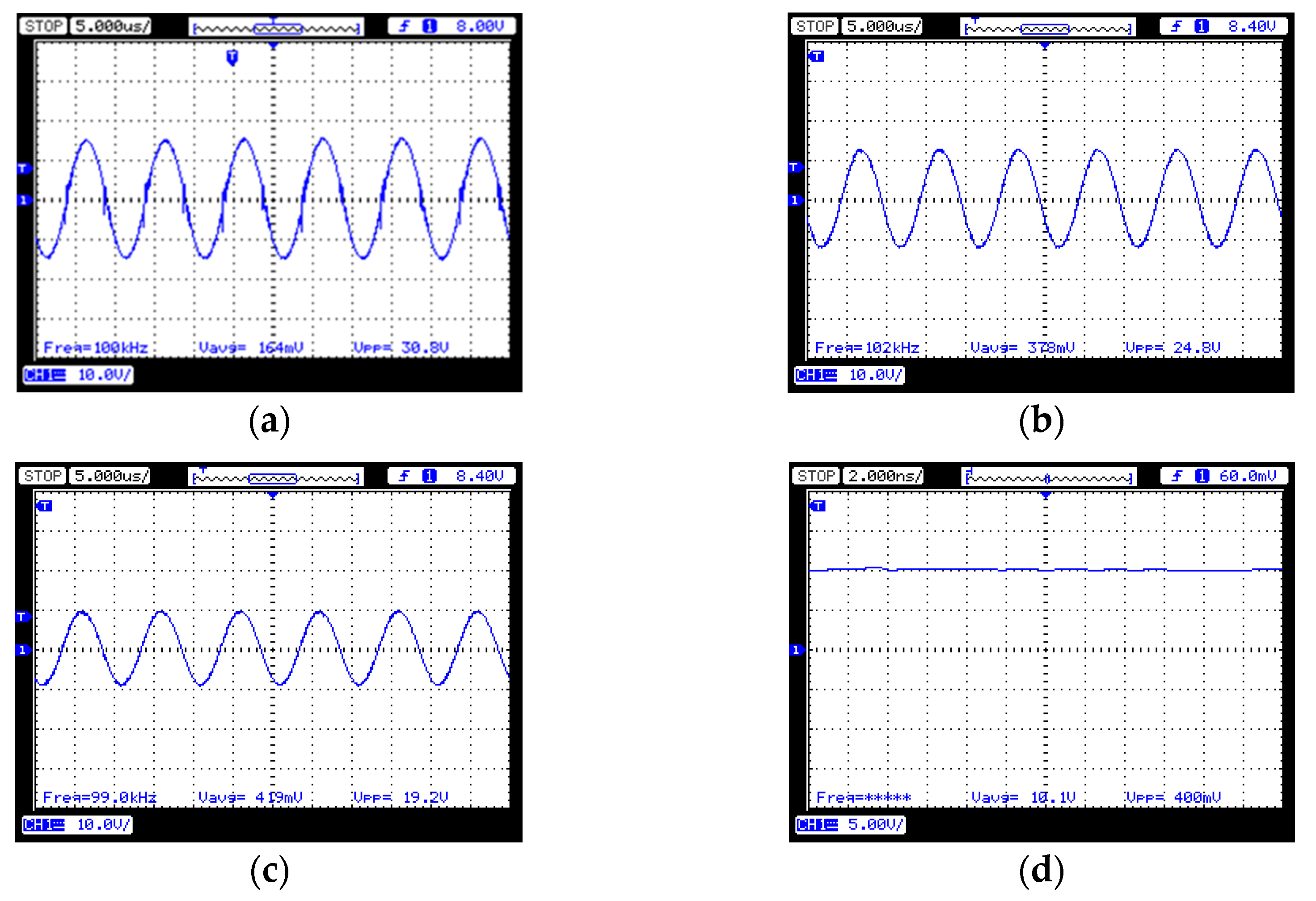
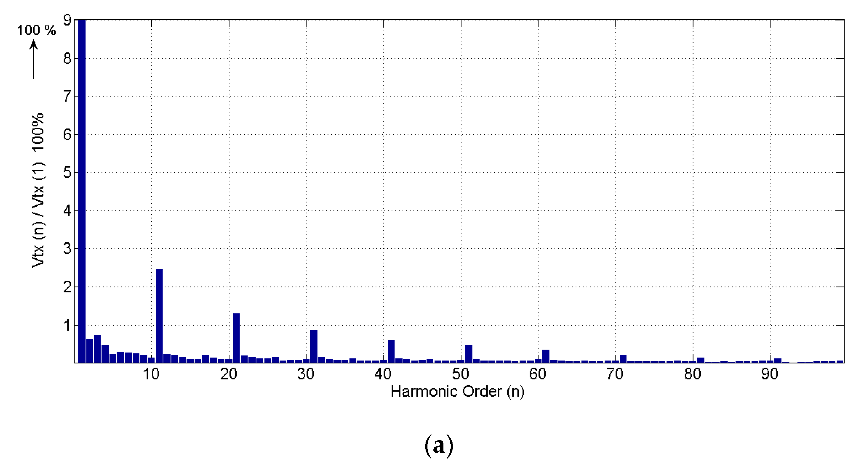
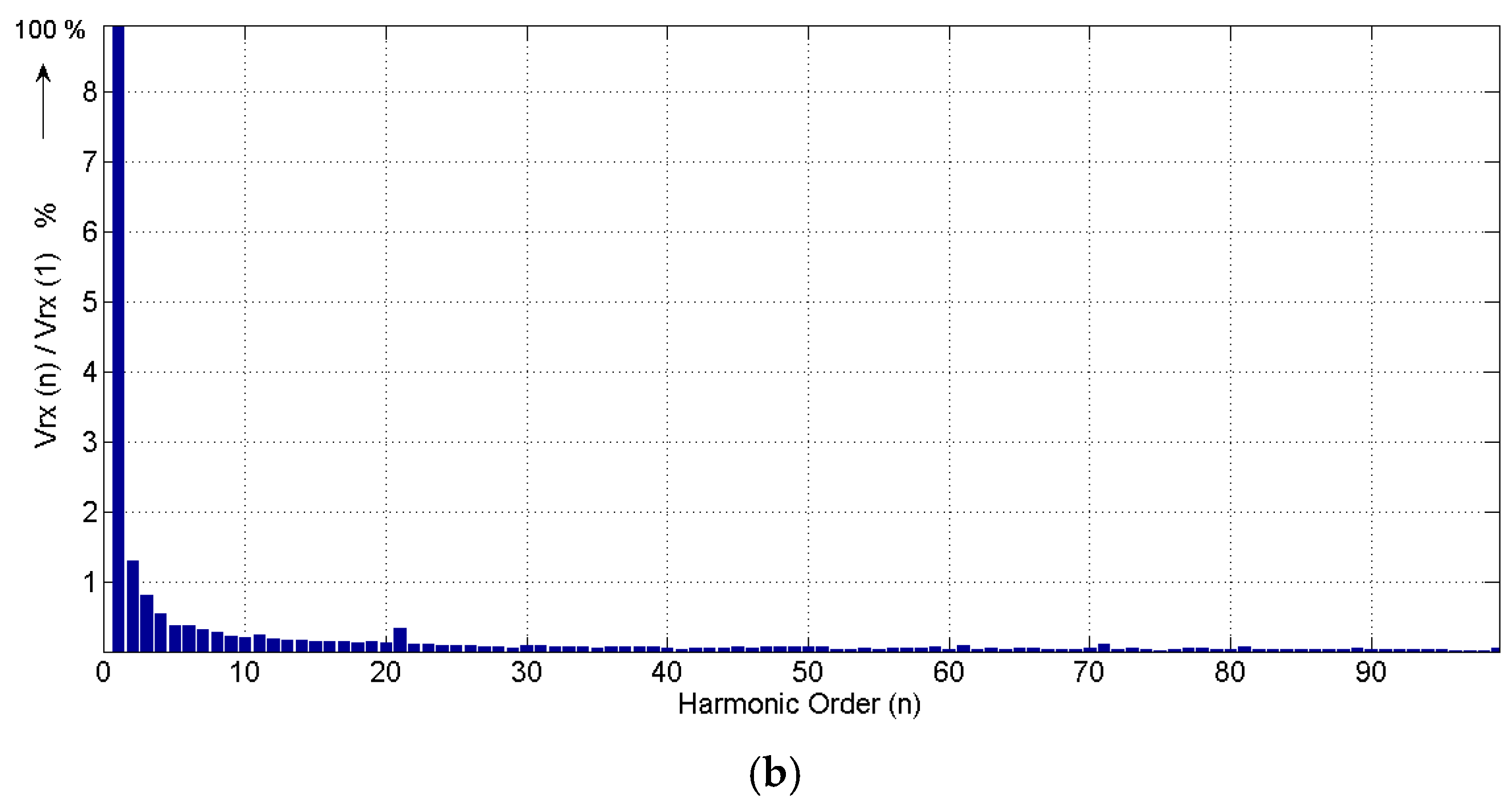
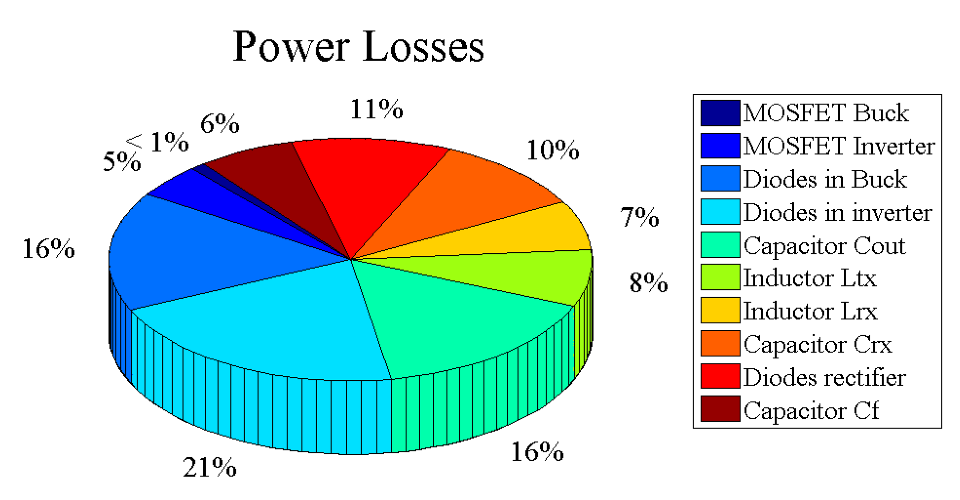
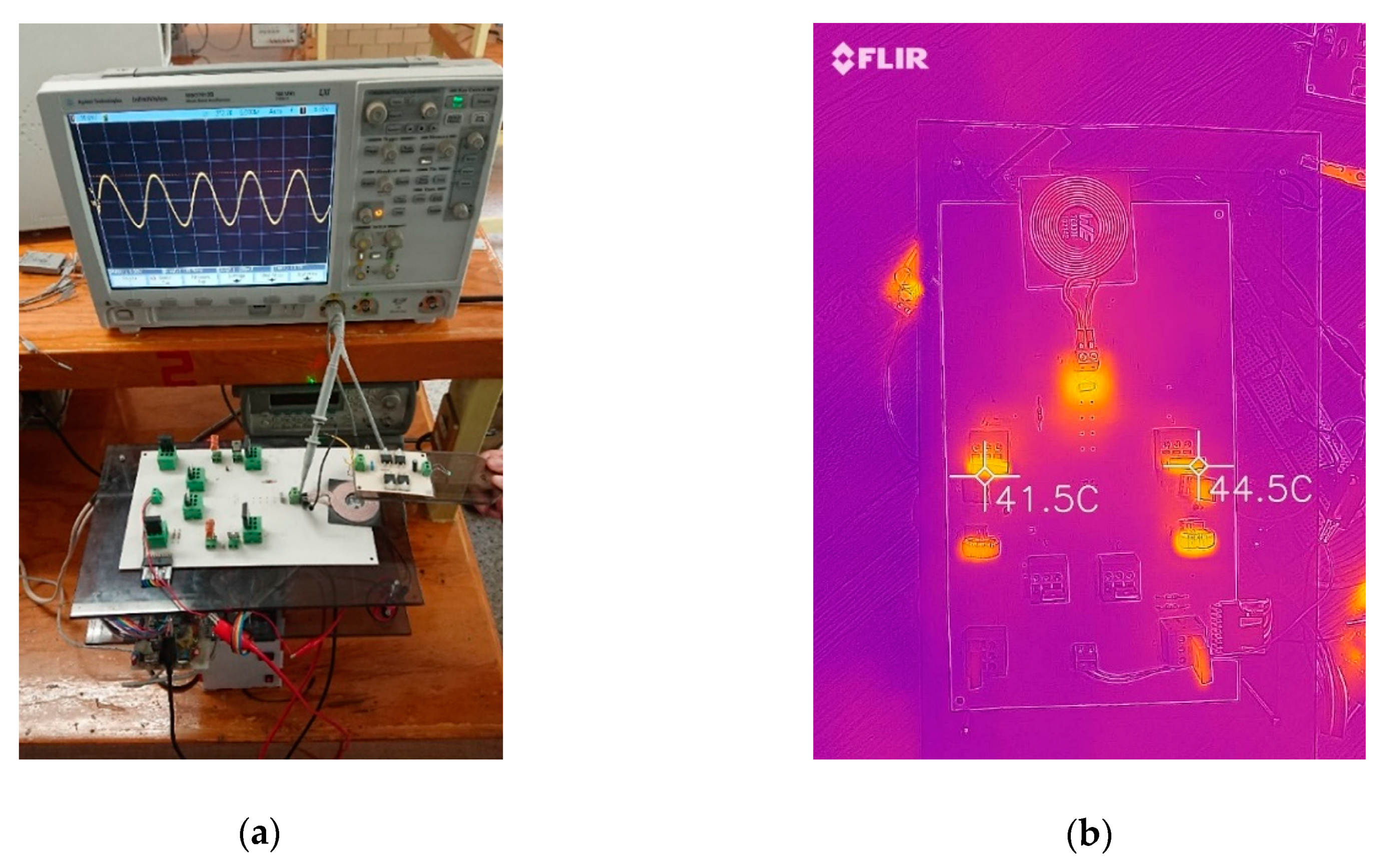
4. Experimental Results

To validate the principle of operation of the proposed converter, a prototype with a maximum nominal power transmission of 15 W was implemented. The variables used in the experiment, the component parameters of the prototype, and the semiconductor device types are listed in Table 2 and Table 3.
A microcontroller STM32F051 was used to obtain the digital control signals at 100 kHz and 500 kHz with an interface implemented with drivers UCC2050 and UCC21530. The results of the experimental test bench were measured using a 100 MHz Mixed signal oscilloscopes MSO7012B and DS01012A from Agilent Technologies.
To validate the wireless energy transmission, inductors 760308111 and WE760308102142 of Wurth-Elektronics were used as transmitter and receptor inductors respectively. This type of inductors is designed with minimal losses and absorption (High Q) and it operates between 100 kHz and 200 kHz at powers up to 200 W. Mosfet CMF1020D was used with a trr of 138 ns with low capacitances, high blocking voltage of 1200 V with Low RDS(on) of 160 mΩ, and continuous drain current of 24A@25°. SiC Schottky diodes, C2D10120, were employed in the rectifier to operate at 100 kHz with low switching losses, and this device has the following parameters: IF(AV) of 31 A with zero reverse recovery current, essentially no switching losses. The parameters indicated on each component ensure minimum switching and conduction losses, switching to the operating frequency and adequate power handling.
To achieve the switching frequency of 500 kHz, the digital signals VG1, VG2, VG3, and VG4 plotted in Figure 9 are used to control the semiconductor devices in the interleaved buck converter and were generated using the microcontroller STMicroelectronics STM32F108.
To validate the wireless energy transmission, the voltage vtx in Ltx is plotted in Figure 10a with an amplitude of 30.8 Vpp. The voltage vrx in Lrx is plotted in Figure 10b for a gap of 15 mm and in Figure 10c for 50 mm, with an amplitude of 24.8 Vpp and 19.2 Vpp, respectively. It can be denoted that the fundamental frequency is 100 kHz according to the switching frequency of VG1 and VG3. The rectified voltage in the output resistive load vo is plotted in Figure 10d, where the average value is 10.1 V with a ripple voltage of 400 mVpp that corresponds to 3.96% of Vo (<10% of Vo).
To find the optimal gap between the couple inductors, an analysis of the voltage vrx in the receptor inductor versus the gap between the inductors was performed. Figure 11 shows the voltage in the receptor circuit according to a variation of D in the interleaved buck operation with different gap conditions. It was found that a maximum energy transfer takes place in the 12 mm to 20 mm gap range. With the results of Figure 11, the coupling factor between the inductors has been calculated, and the result is shown in Figure 12. It can be denoted for the optimal gap that the coupling factor is between 0.65 and 0.53.
To verify the high quality of voltage waveforms, the harmonic components in vtx and vrx were calculated as shown in Figure 13a,b, respectively. It can be denoted that there are no significant components in high frequencies. The measured THD was 3.5% for vtx and 1.97% for vrx, being the power rated at 15 W.
The efficiency of the converter is η = 85.1%, with an input power of 15 W and a total power loss of 2.23 W distributed in the components according to Figure 14. As can be seen, the principal losses occur in the diodes and the capacitors.
Typically, diode switching loss and power loss in the inductor core can be ignored, and only the copper loss in the inductor winding should be considered.
The main component losses are related by the following expressions:
Mosfet conduction losses:
P c o n d u c t i o n = V o r D S R L min P o max
Mosfet switching losses:
P s w i t c h i n g = f S C o M o s f e t R L min V i n max 2 P o max V o 2
Diode conduction losses:
P c o n d u c t i o n = ( 1 V o V i n max ) ( V F V o + r d i o d e R L min ) P o max , P r L = r L V i n max 2 R L min P o max
Power losses in the filter capacitor:
P r C = r C R L ( 1 V o V i n max ) 2 12 f S 2 L 2 P o max
The total power losses are given by
P t o t a l = P c o n d u c t i o n + P s w i t c h i n g + P r L + P r C .
The parasitic parameters of each component, Mosfet (CoMosfet), Diode (VF, rdiode), Inductors (rL), and Capacitors (rC), impact on the total power losses.
Figure 15a shows the prototype in operation with a current demand of 450 mA. A thermal capture of the interleaved buck converter during operation is presented in Figure 15b, showing that main thermal losses take place in inductors LB1 and LB2 and MOSFET’s with temperatures of 41.5 °C and 44.5 °C.

5. Comparison of the Proposed Converter with Other DC–DC Topologies

Table 4 presents a comparison of the proposed topology with five different DC–DC converters [13,14,15,16]. The comparison includes the number of semiconductor devices, energy storage components (inductors and capacitors), the efficiency, and the output power. It can be denoted that the proposed DC–DC converter allows a reduction in the number of energy storage components, allowing a high-efficiency system and a control method that is simple and easy to be implemented. The proposed converter is possible to scale in power maintaining the same topology.

6. Conclusions

The principle of operation of a DC–AC converter for IWPT was presented. The proposed topology includes two buck converters that operate together with a half inverter bridge and a resonant circuit. A sinusoidal waveform with a low THD was obtained being suitable for wireless inductive power transfer. The proposed control strategy uses two PWM burst signals and two PWM complementary signals to synchronize the two buck converters operation, being a simple and effective control method to obtain the defined ideal waveforms. The proposed converter was validated with experimental results in a 15.0 W prototype using two coupled inductors with a gap of 15 mm to 50 mm, being suitable for portable devices battery recharge applications.

Author Contributions

Conceptualization, L.H.-G.; data curation, M.C.-R., L.A.S.-J. and J.G.A.-O.; formal analysis, J.R.-H. and L.H.-G.; investigation, M.C.-R., L.H.-G. and J.R.-H.; methodology, P.G.-L. and I.L.; software, M.C.-R. and L.A.S.-J., supervision and validation, I.L. and J.G.A.-O.; writing, original draft, J.R.-H., L.H.-G. and I.L.; writing, review and editing, L.H.-G., J.R.-H., I.L., and J.G.A.-O. All authors have read and agreed to the published version of the manuscript.

Funding

This research was funded by the Instituto Politécnico Nacional.

Acknowledgments

The authors are grateful to the Instituto Politécnico Nacional (IPN) for their encouragement and kind economic support to realize the research project

Conflicts of Interest

The authors declare no conflict of interest.

Nomenclature

DDuty cycle
MB1MOSFET in Buck 1
MB2MOSFET in Buck 2
LB1Inductor in Buck 1
LB2Inductor in Buck 2
DB1Diode in Buck 1
DB2Diode in Buck 2
MH1, MH2MOSFE’s in leg inverter
CtxCapacitor in parallel resonant circuit in transmitter circuit
LtxTransmitter inductor
CrxCapacitor in parallel resonant circuit in receptor circuit
LrxReceptor inductor
CfOutput filter capacitor
Da, Db, Dc, DdBridge rectifier diodes
VG1, VG3Control signals in half bridge rectifier
V21, VG4Control signals in Buck converters
THBHalf bridge inverter control signals
VBuckBuck converter output voltage
VtxpkTransmitter peak output voltage
VinInput voltage
VinmaxMaximum input voltage
VtxTransmitter output voltage
VrxReceptor input voltage
VFThe threshold voltage
RoOutput load
RLminMinimal load
rDSMosfet On-resistance
rCParasitic resistance of capacitor
rLParasitic resistance of inductor
rdiodeParasitic resistance of diode
VoOutput voltage
IoOutput current
x1, x2, x3, x4State variables
IF(AV)Average forward current
iLB1Current in LB1
iLB2Current in LB2
iLtxCurrent in Ltx
iLrxCurrent in Lrx
ΔVoOutput ripple voltage
ΔIoOutput ripple current
fsSwitching frequency
fBurstBurst signals switching frequency
fHBHalf bridge inverter switching frequency
PoOutput power
PomaxMaximum output power
PconductionConduction power losses
PswitchingSwitching power losses
PrCCapacitor power losses
PtotalTotal power losses
trrReverse recovery time
kCoupling factor in inductors Ltx and Lrx
ηEfficiency in the converter

References

  1. Galizzi, M.; Caldara, M.; Re, V.; Vitali, A. A novel Qi-standard compliant full-bridge wireless power charger for low power devices. In Proceedings of the IEEE Wireless Power Transfer, Perugia, Italy, 15–16 May 2013. [Google Scholar]
  2. Yanjun, L.; Yuzhe, C.; Chung, S.C.; Zhibo, W.; Yi-hua, Z. Charging While Moving: Deploying Wireless Chargers for Powering Wearable Devices. IEEE Trans. Veh. Technol 2018, 67, 11575–11586. [Google Scholar]
  3. Jiejian, D.; Daniel, C.L. A Survey of Wireless Power Transfer and a Critical Comparison of Inductive and Capacitive Coupling for Small Gap Applications. IEEE Trans. Power Electron. 2015, 30, 6017–6029. [Google Scholar]
  4. Mostafa, T.M.; Muharam, A.; Hattori, R. Wireless battery charging system for drones via capacitive power transfer. In Proceedings of the IEEE Workshop on Emerging Technologies: Wireless Power Transfer, Chongqing, China, 20–22 May 2017. [Google Scholar]
  5. Zhang, H.; Chong, Z.; Fei, L. Long-Distance and High-Power Capacitive Power Transfer based on the Double-Sided LC Compensation: Analysis and Design. In Proceedings of the IEEE Transportation Electrification Conference and Expo, Detroit, MI, USA, 19–21 June 2019. [Google Scholar]
  6. Van-Binh, V.; Duc-Hung, T.; Woojin, C. Implementation of the Constant Current and Constant Voltage Charge of Inductive Power Transfer Systems With the Double-Sided LCC Compensation Topology for Electric Vehicle Battery Charge Applications. IEEE Trans. Power Electron. 2018, 33, 7398–7410. [Google Scholar]
  7. Mohammadhossein, A.; Akshay, K.R. Receiver side control for efficient inductive power transfer for vehicle recharging. In Proceedings of the IEEE Transportation Electrification Conference, Pune, India, 13–15 December 2017. [Google Scholar]
  8. Chih-Cheng, H.; Chun-Liang, L. Wireless Power and Bidirectional Data Transfer Scheme for Battery Charger. IEEE Trans. Power Electron. 2018, 33, 4679–4689. [Google Scholar]
  9. Minfan, F.; Chengbin, M.; Xinen, Z. A Cascaded Boost–Buck Converter for High-Efficiency Wireless Power Transfer Systems. IEEE Trans. Ind. Informat. 2014, 10, 1972–1980. [Google Scholar]
  10. Erdem, A.; Kerim, C.; Dariusz, C. Analysis of cascaded multi-output-port converter for wireless plug-in Hybrid/On-Board EV chargers. In Proceedings of the IEEE Applied Power Electronics Conference and Exposition, Long Beach, CA, USA, 20–24 March 2016. [Google Scholar]
  11. Xinhong, F.; Ming, L.; Zefan, T.; Chengbin, M. Design procedure of a class E2 DC-DC converter for megahertz wireless power transfer based on a compact class E current-driven rectifier. In Proceedings of the IEEE International Symposium on Industrial Electronics, Edinburgh, UK, 19–21 June 2017. [Google Scholar]
  12. Tomoharu, N.; Xiuqin, W.; Elisenda, B.; Alarcón, E.; Kazimierczuk, M.K.; Sekiya, H. Analysis and Design of Loosely Inductive Coupled Wireless Power Transfer System Based on Class-E2 DC-DC Converter for Efficiency Enhancement. IEEE Trans. Circuits Syst. I Reg. Pap. 2015, 62, 2781–2791. [Google Scholar]
  13. Xuejian, G.; Yue, S.; Chunsen, T.; Zhihui, W.; Zhou, X. Loss analysis and efficiency optimization of buck converter in wireless charging system for EVs. In Proceedings of the IEEE Workshop on Emerging Technologies: Wireless Power Transfer, Chongqing, China, 20–22 May 2017. [Google Scholar]
  14. Carbajal-Retana, M.; Camacho-Cabrera, J.; Hernandez-González, L.; Tapia-Hernández, A. Buck-inverter converter for application in inductive wireless transmission. In Proceedings of the IEEE International Conference on Power Electronics, Cholula Puebla, Mexico, 24–26 October 2018. [Google Scholar]
  15. Yungtaek, J.; Jovanovic, M.M. A contactless electrical energy transmission system for portable-telephone battery chargers. IEEE Trans. Ind. Electron. 2003, 50, 520–527. [Google Scholar] [CrossRef] [Green Version]
  16. Jun-Young, L.; Byung-Moon, H. A Bidirectional Wireless Power Transfer EV Charger Using Self-Resonant PWM. IEEE Trans. Power Electron. 2015, 1784–1787. [Google Scholar]
  17. Liu, C.; Hu, A.P.; Nair, K.C. Modelling and analysis of a capacitively coupled contactless power transfer system. IET Power Electron. 2011, 808–815. [Google Scholar] [CrossRef]
  18. Theodoridis, M.P. Effective Capacitive Power Transfer. IEEE Trans. Power Electron. 2012, 4906–4913. [Google Scholar] [CrossRef]
Figure 1. Proposed DC–DC converter.
Electronics 09 00949 g001
Figure 2. Ideal waveforms for one fundamental switching period of the proposed converter.
Electronics 09 00949 g002
Figure 3. Mode 1 of DC–DC converter.
Electronics 09 00949 g003
Figure 4. Mode 2 of DC–DC converter.
Electronics 09 00949 g004
Figure 5. Simulation results for signals VG1, VG2, VG3, and VG4.
Electronics 09 00949 g005
Figure 6. Simulation results for iLtx and iLrx. Supply: 25 V, Output: 10 V.
Electronics 09 00949 g006
Figure 7. Simulation results for vrx. Supply: 25 V, Output: 10 V.
Electronics 09 00949 g007
Figure 8. Simulation results for output voltage and current vo, io. Supply: 25 V, Output: 10 V.
Electronics 09 00949 g008
Figure 9. Experimental results for control signals VG1 (yellow), VG2 (blue), VG3 (green), and VG4 (red). Duty Cycle: 0.6, Supply: 25 V, Output: 10 V.
Electronics 09 00949 g009
Figure 10. Experimental results. (a) vtx, (b) vrx for a gap of 32 mm between coupled inductors, (c) vrx for a gap of 20 mm between coupled inductors and (d) output DC voltage in Ro. Supply: 25 V Output: 10 V.
Electronics 09 00949 g010
Figure 11. Voltage in Lrx vs. D and the gap between inductors.
Electronics 09 00949 g011
Figure 12. Coupling factor k vs. the gap between inductors.
Electronics 09 00949 g012
Figure 13. Harmonic content for (a) vtx and (b) vrx.
Electronics 09 00949 g013aElectronics 09 00949 g013b
Figure 14. Power losses in the components of the converter.
Electronics 09 00949 g014
Figure 15. Views of the prototype: (a) View of the operating prototype, (b) Interleaved Buck converter thermal image.
Electronics 09 00949 g015
Table 1. Simulation variables and component parameters. PWM: Pulse Width Modulation.
QuantityValue
Supply voltage Vin25 V
Output voltage V010 V
Output power Po15 W
Ripple voltage ΔVo10% of Vo
Switching frequency of burst PWM signal fBurst500 kHz
Switching frequency of inverter leg fHB100 kHz
Inductors LB1 and LB2130 µH
Capacitor Ctx0.47 µF
Capacitor Crx220 nF
Capacitor Cf4.7 µF
Inductor Ltx6.3 µH
Inductor Lrx12 µH
Output load Ro330 Ω
Table 2. Variables and component parameters of the experiment.
QuantityValue
Source voltage Vin25.0 V
Output voltage Vo10.0 V
Switching frequency of burst PWM signal fBurst500 kHz
Switching frequency of inverter leg fHB100 kHz
Inductors LB1 and LB2130 µH
Capacitor Ctx0.47 µF
Capacitor Crx220 nF
Capacitor Cf4.7 µF
Inductor Ltx6.3 µH
Inductor Lrx12.0 µH
Output load Ro330 Ω
Table 3. Types of semiconductor devices.
DeviceType
MOSFETsCMF10120D
Diodes, DB1 and DB2C2D10120
Diodes Da, Db, Dc and Dd1N5822
Table 4. Comparison with other topologies.
TopologyProposed DC–DC ConverterCascaded Buck-Boost Converter [9]Contactless Electrical Energy Transmission System [15]Bidirectional WPT EV Charger Using Self-Resonant PWM [16]Capacitively Coupled
Contactless Power Transfer System [17]
Capacitive Power Transfer [18]
Factor
Semiconductor devices transmitter-receptor44(only in receptor)242–42–4
Energy storage components323386
Switching frequency500 kHz20 kHz67–140 kHz20.3 kHz840 kHz1 MHz
Efficiency η85.1%74%60–70%88%41%80%
Output Power15 W40 W4.5 W6.6 kW7.6 W25 W
AdvantagesThe proposed topology and control method are simple and achieve high efficiency This topology provides an optimal impedance for minimal
power reflection
This topology allows bidirectional power flow through the inductancesThe high power makes it suitable for electric vehicle applicationsZero Voltage Switching (ZVS) is used to reduce lossesThe
design algorithm ensures reduction of the system
size
Major DrawbacksWork in progress to achieve higher output power Electromagnetic components could be reduced by increasing the switching frequency The distortion in voltage waveforms avoids a higher efficiency in the system Electromagnetic components could be reduced by increasing the switching frequency The power efficiency is too low under heavy load conditionsSome losses may be compensated by using a ZVS

