Article

Analytical Drain Current Model for a-SiGe:H Thin Film Transistors Considering Density of States

by
Silvestre Salas-Rodríguez
1,
Francisco López-Huerta
2,3,
Agustín L. Herrera-May
1,3,
Joel Molina-Reyes
4 and
Jaime Martínez-Castillo
1,*
1
Research Center in Micro and Nanotechnology, Universidad Veracruzana, Calzada Ruiz Cortines 455, Boca del Río, Ver 94294, Mexico
2
Faculty of Electrical and Electronic Engineering, Universidad Veracruzana, Calzada Ruiz Cortines 455, Boca del Río, Ver 94294, Mexico
3
Master in Applied Engineering, Faculty of Construction and Habitat Engineering, Universidad Veracruzana, Calzada Ruiz Cortines 455, Boca del Río, Ver 94294, Mexico
4
Electronic Department, National Institute of Astrophysics, Optics and Electronics (INAOE), Luis Enrique Erro 1, Santa María Tonanzintla, Puebla 72840, Mexico
*
Author to whom correspondence should be addressed.
Electronics 2020, 9(6), 1016; https://doi.org/10.3390/electronics9061016
Submission received: 27 May 2020 / Revised: 15 June 2020 / Accepted: 16 June 2020 / Published: 18 June 2020
(This article belongs to the Special Issue New CMOS Devices and Their Applications)

Abstract

:
Thin film transistors (TFTs) fabricated on flexible and large area substrates have been studied with great interest due to their future applications. Recent studies have developed new semiconductors such as a-SiGe:H for fabrication of high performance TFTs. These films have important advantages, including deposition at low temperatures and low pressures, and higher carrier mobilities. Due to these advantages, the a-SiGe:H films can be used in the fabrication of TFTs. In this work, we present an analytical drain current model for a-SiGe:H TFTs considering density of states and free charges, which describes the current behavior at sub-and above- threshold region. In addition, 2D numerical simulations of a-SiGe:H TFTs are developed. The results of the analytical drain current model agree well with those of the 2D numerical simulations. For all characteristics of the drain current curves, the average absolute error of the analytical model is close to 5.3%. This analytical drain current model can be useful to estimate the performance of a-SiGe:H TFTs for applications in large area electronics.

1. Introduction

Thin film transistors (TFTs) are key devices to develop large area electronics applications such as active matrix liquid crystal displays (AMLCD) [1,2,3], wearable sensors [4,5] and passive tags RFID (radio frequency identification) [6,7,8]. Nowadays, TFT technology is based on amorphous silicon (a-Si), polysilicon (poly-Si) and IGZO (indium-gallium-zinc oxide) semiconductors. The a-Si TFTs offer small electron mobilities (<1 cm2/Vs), and thus low switching speed [9]. The other hand, poly-Si TFTs are devices with high performance, but they are fabricated at higher temperatures (500–600 °C) [10,11,12], while IGZO TFTs have moderate mobilities (>10 cm2/Vs) and low temperature of fabrication [13]. However, this semiconductor is only used for the fabrication of n-type devices, for p-type is used a different semiconductor, such as SnO [14]. To overcome these limitations, hydrogenated amorphous silicon-germanium (a-SiGe:H) films can be used to fabricate TFTs at low temperature of deposition (<300 °C) by PECVD technique. This allows carrier mobilities higher than 1 cm2/Vs caused by the incorporation of germanium and hydrogen atoms. In addition, a-SiGe:H TFTs can have an ambipolar behavior, allowing their operation into either as n- or p-type [15]. In order to design a-SiGe:H TFTs for specific applications, it is necessary to predict the behavior of their drain currents. Shur et al. [16] reported a physical drain current model for n- and p-channels hydrogenated amorphous silicon and polysilicon staggered bottom-gate top-contact TFTs. This model was implemented into an AIM-SPICE circuit simulator. However, it is adapted from MOSFET model and it does not include semiconductor density of states. Chen et al. [17] reported an analytical drain current model for both triode and saturation region of operation for a-Si:H TFTs considering semiconductor density of states and an effective temperature approach. However, this model registered a high error between measurements and modeled results. Liu et al. [18] presented an analytical drain current model for a-Si:H TFTs based on surface potential, which was compared with numerical simulations considering free and localized carrier densities into the semiconductor. Colalongo et al. [19] designed an analytical drain current model for a-Si:H TFTs based on deep and tail states in both semiconductors, which describe the behavior at sub-threshold and above-threshold mode of operation.
In this paper, we develop an analytical drain current model for a-SiGe:H TFTs that considers free and localized charges into semiconductor and its characteristic temperatures, which can represent the behavior at sub-threshold and above-threshold regions of operation without using fitting parameters. In addition, 2D numerical simulations using finite element method of the output and transfer characteristics of bottom-gate top-contact coplanar a-SiGe:H TFTs are reported. The results of our analytical drain current model agree well with respect to those of the numerical simulations. In Section 2, electrostatic analysis and derivation of expressions for electric field and drain current are explained. In Section 3, comparison of our model and simulation results are presented. Finally, the conclusions are discussed in Section 4.

2. Analytical Drain Current Model for a-SiGe:H TFTs

2.1. Density of Estates of Amorphous Semiconductors

The density of states, g(E), of an amorphous semiconductor thin film consists of four energy bands over the bandgap: two tail bands and two deep bands. Tail bands consist of a donor-like valence band, gTA(E), and an acceptor-like conduction band, g T D ( E ) . On the other hand, deep bands are composed of a donor-like valence band, g G A ( E ) , and an acceptor-like conduction band, g G D ( E ) , which are represented as follow, [20]:
g ( E ) = g T A ( E ) + g T D ( E ) + g G A ( E ) + g G D ( E )
g T A ( E ) = N T A exp [ ( E E C ) / W T A ]
g T D ( E ) = N T D exp [ ( E V E ) / W T D ]
g G A ( E ) = N D A exp [ ( ( E E G A ) / W G A ) 2 ]
g G D ( E ) = N D D exp [ ( ( E E G D ) / W G D ) 2 ]
where E is the trap energy, EC and Ev are the conduction and valence band energy, respectively; WTA (kTtail) and WTD (kTtail) are acceptor and donor characteristic decay energy for the tail band, respectively; WGA (kTdeep) and WGD (kTdeep) are acceptor and donor characteristic decay energy for the deep band, respectively; NTA, NTD, NDA and NDD are the conduction and valence band edge intercept densities for the tail and deep band, respectively.

2.2. Analytical Drain Current Model

Figure 1a shows a schematic cross section of a n-type coplanar bottom-gate top-contact a-SiGe:H TFT with SiO2 as gate insulator and a-Ge:H n+ layers for drain and source extensions. In this Figure, Tox and Tsc are the gate oxide and semiconductor thickness, respectively. Figure 1b depicts the diagram of energy band for MIS (metal-insulator-semiconductor) region for this device working under accumulation regimen, when a positive gate potential (VG) is applied. For this Figure, EC and EV are energy levels of conduction and valence bands, respectively; EFm, and EFn are the Fermi energy levels for metal, intrinsic and n-type semiconductor, respectively; φS and φCH(x) are surface and channel potential; and φF0(x) is the potential between Ec and EFn.

2.2.1. Derivation of Electric Field

Taking into account the free and localized electron concentration for an n-type amorphous semiconductor, the Poisson’s equation in one dimension, along the x direction, can be expressed as:
2 ϕ ( x ) x 2 = ρ ( x ) ε s c = q ε s c ( n f r e e ( x ) + n d e e p ( x ) + + n d e e p ( x ) )
where q is the electron charge, ϕ(x) is the potential across the active layer, ρ(x) is the total charge density, ɛsc is the permittivity constant of the semiconductor layer, nfree(x), ndeep(x) and ntail(x) are the free, deep and tail electron concentrations, respectively. These concentrations for a-SiGe:H layer can be expressed as:
n f r e e ( x ) = N f r e e exp [ q ( ϕ ( x ) V CH ϕ F 0 ) k T f r e e ]
N f r e e = N C g ( T / T f r e e ) k T π s i n ( π T / T f r e e )
n d e e p ( x ) = N d e e p exp [ q ( ϕ ( x ) V CH ϕ F 0 ) W G A ]
N d e e p = g G A g ( T / T d e e p ) k T π s i n ( π T / T d e e p )
n t a i l ( x ) = N t a i l exp [ q ( ϕ ( x ) V CH ϕ F 0 ) W T A ]
N t a i l = g T A g ( T / T d e e p ) k T π s i n ( π T / T d e e p )
where NC is the free electron concentration, VCH is the potential along the channel, q is the electron charge, k is Boltzmann constant, T is a reference temperature and g is the degeneration factor which depends of the temperature ratio (T/Teff) as exponential expression.
In order to simplify the analysis, an effective carrier concentration (Neff) instead of free, deep or tail carrier concentrations (Nfree, Ndeep or Ntail), which are computed with Equations (8), (10) or (12) equations, respectively, is proposed. In the same way, an effective characteristic temperature (Teff) instead of free, deep or tail temperature (Tfree, Tdeep or Ttail), respectively, is used.
To derivate the electric filed as function of electrostatic potential, it is necessary to solve the following Poisson´s equation:
2 ϕ ( x ) x 2 = ρ ( x ) ε s c = q ε s c n e f f ( x )
By employing the next expression to change the integration variable, from x to ϕ(x):
d d x [ ( d ϕ ( x ) d x ) 2 ] = 2 ( d ϕ ( x ) d x ) ( d 2 ϕ ( x ) d x 2 )
By integrating both sides in Equation (14) and applying the square root, we have:
d ϕ ( x ) d x = 2 ( d ϕ ( x ) d x ) ( d 2 ϕ ( x ) d x 2 ) d x = 2 ( d 2 ϕ ( x ) d x 2 ) d ϕ ( x )
By substituting Equation (13) into Equation (15) and applying the boundary conditions from x = 0 (ϕS (x)) to x = TSC (ϕB(x)), the electric field as a function of ϕ(x) is expressed as:
E ( ϕ ( x ) ) = d ϕ ( x ) d x = 2 ϕ ( x = T s c ) = ϕ B ϕ ( x = 0 ) = ϕ S q ε s c n e f f ( x ) d ϕ ( x ) = 2 N e f f k T e f f ε s c ( n e f f ( ϕ S ( x ) ) n e f f ( ϕ B ( x ) ) )
where neff is the effective electron density, Teff is the effective characteristic temperature, ε s c   is the semiconductor permittivity, ϕS(x) is the electrostatic potential in the gate insulator/semiconductor interface, ϕB(x) is the electrostatic potential in the semiconductor/passivation layer interface, which is neglected because is close to zero. Thus, the transversal electric field through an amorphous semiconductor, at x direction, is given by:
E ( ϕ ( x ) ) = 2 N e f f k T e f f ε s c exp [ q ( ϕ S V CH ϕ F 0 ) 2 k T e f f ]

2.2.2. Derivation of Drain to Source Current in Subthreshold Region, IDS_sub

In the subthreshold region operation of a-SiGe:H TFT, that is gate to source voltage, VGS, is less than threshold voltage, VTH, but larger than the flat band voltage, VFB, (VFB < VGS < VTH), most of the carriers are free electrons, because of deep and tail localized carriers are trapped into semiconductor defects. Therefore, it is necessary to apply a larger VGS in order to generate a higher transversal electric field to the active layer to set free those charges. In addition, for this semiconductor (see Table 1) the localized energy characteristics (kTtail and kTdeep) are higher than the free energy characteristic (kTfree). Thus, ρ ( x ) for an a-SiGe:H TFT at subthreshold operation can be obtained by:
ρ ( x ) q = n e f f ( x ) n f r e e ( x )
In order to derive the drain to source current in subthreshold regimen, IDS_sub, is employed the gradual channel approximation expression, which is given by:
I D S _ s u b = W d V C H ( y ) d y x = 0 x = T s c σ n ( x ) d x = W d V C H ( y ) d y ϕ ( x = t s c ) ϕ ( x = 0 ) q μ 0 n f r e e ( ϕ ( x ) ) E ( ϕ ( x ) ) d ϕ ( x )
where W is the channel width of TFT, σn(x) is the n-type channel conductivity of a-SiGe:H, E(φ(x)) is the electric field dependent of potential at x direction, and μ0 is the carrier mobility of semiconductor.
The final expression for drain to source current at region of subthreshold for an a-SiGe:H TFT is computing solving Equation (19), step-by-step at Appendix A, considering Neff = Nfree and Teff = Tfree, as follows:
I D S _ s u b ( N f r e e , T f r e e ) = μ 0 W L A f r e e B f r e e ( C O X 2 ε s c N f r e e k T f r e e ) C f r e e [ 1 C f r e e + 1 ( ( δ V S D ) C f r e e + 1 ( δ V S S ) C f r e e + 1 ) + 1 q B f r e e ( ( δ V S D ) C f r e e ( δ V S S ) C f r e e ) ]
with:
A f r e e = N c 2 N f r e e k T f r e e ε s c
B f r e e = 1 k T 1 2 k T f r e e
C f r e e = 2 k T f r e e B f r e e
δ V S D = V G S V F B V D
δ V S S = V G S V F B V S

2.2.3. Derivation of Drain Current at Above Threshold Region, IDS_abv

Above threshold region of a-SiGe:H TFT operation, that is when VGS > VTH, free and localized charges are taken in to account due to the applied gate to source voltage generates a strong transversal electric field to the active layer which produces an accumulation of both carriers in the semiconductor/gate-insulator interface. However, in this semiconductor ndeep(x) << ntail(x). Thus, we obtained the following equation:
ρ ( x ) q = n e f f ( x ) n f r e e ( x ) + n t a i l ( x )
Poisson’s equation is applied as follows:
2 ϕ ( x ) x 2 = ρ ( x ) ε s c q ε s c ( n f r e e ( x ) + n t a i l ( x ) )
By using the gradual channel approximation Equation (19) and the procedure in Appendix A, taking into account free and tail localized charges along the semiconductor, we can derive the drain to source current for the above threshold region, IDS_abv, as follows:
I D S _ a b v = I D S ( N f r e e , T f r e e ) + I D S ( N t a i l , T t a i l ) = I D S ( N f r e e , T f r e e ) + μ 0 W L A t a i l B t a i l ( C O X 2 ε s c N t a i l k T t a i l ) C t a i l [ 1 C t a i l + 1 ( ( δ V S D ) C t a i l + 1 - ( δ V S S ) C t a i l + 1 ) + 1 q B t a i l ( ( δ V S D ) C t a i l - ( δ V S S ) C t a i l ) ]
with
A t a i l = N c 2 N t a i l k T t a i l ε s c
B t a i l = 1 k T 1 2 k T t a i l
C t a i l = 2 k T t a i l B t a i l

2.2.4. Total Analytical Drain Current Model

The final unified analytical drain current model for a-SiGe:H TFTs takies into account the sub-threshold and above-threshold regions, which it considers the density of states of such amorphous semiconductor and free electrons, is estimated by adding IDS_sub and IDS_abv with the following expression:
I D S = 1 ( 1 I D S _ s u b + 1 I D S _ a b v )

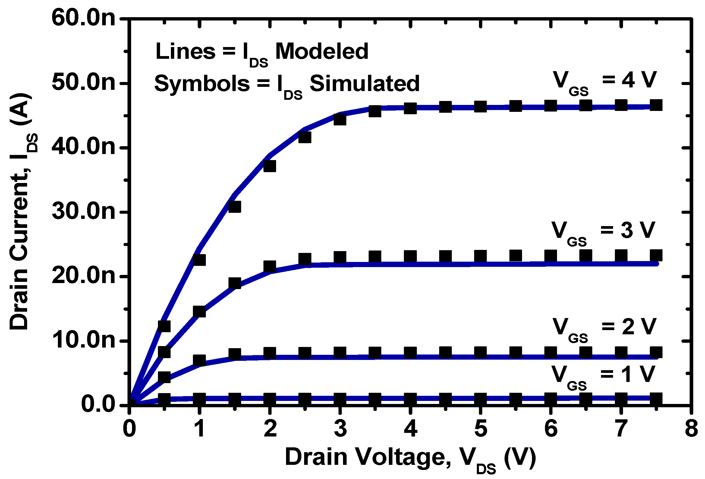
3. Results and Discussion

In order to compare the results of our analytical drain current model, we develop 2D numerical simulations for bottom-gate top-contact coplanar a-SiGe:H TFTs using Silvaco TCAD software through Atlas and Devedit tools (Santa Clara, CA, USA) [21]. These simulation tools use finite element method to perform the electrostatic analysis. Figure 2 shows a schematic view of the cross-section of the proposed device and its main geometrical parameters. The substrate is silicon oxide with a thickness TSUB = 200 nm. The gate and drain/source electrodes are aluminum with thickness TG and TD/S of 100 nm, respectively. SiO2 is used as gate insulator with a thickness TOX = 80 nm. An overlap length between gate and drain/source electrodes of LOV = 10 nm is used. Then, a thin film of a-SiGe:H as active layer or semiconductor with a thickness TSC = 100 nm and a length channel L = 75 µm is used. The width of the active layer W = 30 µm is used for calculation. A layer of high doped germanium as drain/source extension region with thickness TEXT = 40 nm and length LD/S = 2 µm are employed to get a good ohmic contact with the semiconductor. Finally, SiN4 as passivating dielectric layer with TPASS = 200 nm is used in order to reduce broken bonds of the a-SiGe:H surface and carriers recombination.
The parameters for semiconductor and gate insulator layers considered in the numerical simulations and analytical drain current model are listed in Table 1. Furthermore, defects parameters that define the density of states of a-SiGe:H layer used for simulations and modeling are shown in Table 2. Some of those values were taken from [20].
Figure 3 shows the comparison of modeled (lines) and simulated (symbols) characteristics IDS vs VDS for VGS = 1, 2, 3 and 4 Volts. It can be seen that the model is able to represent the behavior of the drain current at the sub-threshold and above-threshold regions for each curve corresponding to different VGS values with a small error for the whole VDS range.
Figure 4 shows the absolute and average error between IDS characteristics modeled and simulated presented, which is computed with Equation (33). It can be seen; the maximum absolute error occurs for the IDS curve when VDS = 0.5 V and VGS = 4 V which is 9.8%. In addition, the average absolute error for all values of VGS is 5%, approximately.
E r r o r ( % ) = 100 ( a b s ( I D S ( s i m u l a t e d ) - I D S ( modeled ) ) I D S ( modeled ) )
Figure 5 shows the comparison of the modeled (lines) and simulated (symbols) output characteristics IDS vs VGS for VDS = 0.1, 1, 2, 3 and 4 Volts. It can be seen that there exist a good fit between modeled and simulated IDS curves for both linear (VDS = 0.1 Volts, VGS > VTH) and saturation (VDS > VGS – VTH, VGS > VTH) regions of operation for a-SiGe:H TFT.

4. Conclusions

In this paper, was developed an analytical drain current model for a-SiGe:H TFTs that shows very good agreement with 2D numerical simulations which were used to validate it. The model considers free and localized charges into a-SiGe:H layer, characteristic temperature dependence and is able to work for sub- and above- threshold region of operation with a small absolute average error. In this sense, the proposed model has implication for development and prediction of electrical performance of TFTs at low frequencies based on amorphous semiconductors, such as a-SiGe:H, which is requested for analysis and design of circuits for large area and flexible electronic systems. Future work will include the fabrication and characterization of a-SiGe:H thin films transistors devices.

Author Contributions

S.S.-R., F.L.-H., and J.M.-C. develop the analytic drain current model. S.S.-R. and J.M.-R. made the simulation of thin film transistors using the INAOE fabrication process. S.S.-R., A.L.H.-M., F.L.-H., J.M.-R., and J.M.-C. wrote all the sections of the paper. All authors have read and agreed to the published version of the manuscript.

Funding

This research was funded by project PRODEP “Modelado y Desarrollo de Microsensores CMOS-MEMS para la detección de diabetes”.

Acknowledgments

This work was supported by National Council of Science and Technology (CONACYT), México, through scholarship 386526, and by Program of Doctorate in Materials and Nanoscience of the Research Center in Micro and Nanotechnology of University of Veracruz (MICRONA-UV), México.

Conflicts of Interest

The authors declare no conflict of interest.

Appendix A

By substituting Equations (7) and (17) in Equation (19), we obtain:
I DS _ sub = W d V C H ( y ) d y ϕ ( x = t s c ) = ϕ B ϕ ( x = 0 ) = ϕ S q μ 0 N f r e e exp [ q ( ϕ ( x ) V C H ϕ F 0 ) k T f r e e ] 2 N e f f k T e f f ε s c exp [ q ( ϕ ( x ) V C H ϕ F 0 ) 2 k T e f f ] d ϕ ( x )
Then, by integrating for ϕ(x) and evaluating from ϕ(x = 0) = ΦS to ϕ(x = TSC) = ΦB, we obtain:
I D S = μ 0 W d V C H ( y ) d y [ A e f f B e f f [ exp [ q B e f f ( ϕ S V C H ϕ F 0 ) ] exp [ q B e f f ( ϕ B V C H ϕ F 0 ) ] ] ]
where:
A e f f = N C 2 N e f f k T e f f ε s c
B e f f = 1 k T f r e e 1 2 k T e f f
However, the second term inside of Equation (A2) is neglected (ϕB = 0). Thus, Equation (A2) can be rearranged as follows:
I D S = μ 0 W d V C H ( y ) d y A e f f B e f f exp [ q B e f f ( ϕ S V C H ( y ) ϕ F 0 ) ]
By integrating Equation (A5) with respect to y at both sides, and by evaluating the boundary conditions from y = 0 (source voltage, VS) to y = L (drain voltage, VD) in order to solve VCH(y), we obtain:
y = 0 y = L I D S d y = μ 0 W V C H ( y = 0 ) = V S V C H ( y = L ) = V D [ A e f f B e f f exp [ q B e f f ( ϕ S V C H ( y ) ϕ F 0 ) ] ] d V C H ( y )
Then, by applying the Gauss’s Law along the Metal-Oxide-Semiconductor structure, and by substituting the electric field expression, we obtain:
V G S = V F B + ϕ s + ε s c E ( ϕ ( x ) ) C o x = V F B + ϕ s + 2 ε s c N e f f k T e f f C o x exp [ q ( ϕ S V C H ( y ) ϕ F 0 ) 2 k T e f f ]
where COX is the capacitance due to gate oxide per area unit, ϕs is surface potential at the oxide/semiconductor interface and VFB is flat band voltage.
V G S V F B ϕ ( x ) 2 ε s c N e f f k T e f f C o x = exp [ q ( ϕ S V C H ( y ) ϕ F 0 ) 2 k T e f f ]
By rewriting Equation (A8) as function of VCH(y), we obtain:
log e [ C o x ( V G S V F B ϕ ( x ) ) 2 ε s c N e f f k T e f f ] = q ( ϕ S ϕ F 0 V C H ( y ) ) 2 k T e f f
2 k T e f f q log e [ C O X 2 ε s c N e f f k T e f f ( V G S V F B ϕ S ) ] + ϕ S ϕ F B = V C H ( y )
By differentiating VCH(y) for ϕ S ( y ) from Equation (A7), we obtain:
d V C H ( y ) d ϕ S ( y ) = 2 k T e f f q 1 V G S V F B ϕ S + 1
Substituting Equations (A10) and (A11) in Equation (A6), we get:
y = 0 y = L I D S d y = μ 0 W V S V D [ A e f f B e f f exp [ q B e f f ( ϕ S V C H ( y ) ϕ F 0 ) ] ] d V C H ( y ) d ϕ S d ϕ S
y = 0 y = L I D S d y = μ 0 W V S V D [ A e f f B e f f exp [ ( 2 k T e f f B e f f log e [ C O X 2 ε s c N e f f k T e f f ( V G S V F B ϕ S ) ] ) ] ] ( 2 k T e f f q ( V G S V F B ϕ S ) + 1 ) d ϕ S
By rewriting Equation (A13), we obtain:
I D S ( N e f f , T e f f ) = μ 0 W A e f f B e f f V C H ( y = 0 ) = V S V C H ( y = L ) = V D [ ( [ ( C O X ε s c ε s c 2 N e f f k T e f f ) 2 k T e f f B e f f ( V G S V F B ϕ S ) 2 k T e f f B e f f ] ) ] ( 2 k T e f f q ( V G S V F B ϕ S ) + 1 ) d ϕ S
Finally, solving Equation (A14), we derive I D S ( N e f f , T e f f ) , which is given by:
I D S ( N e f f , T e f f ) = μ 0 W A e f f B e f f ( C O X ε s c ε s c 2 N e f f k T e f f ) 2 k T e f f B e f f [ V C H ( y = 0 ) = V S V C H ( y = L ) = V D ( V G S V F B ϕ S ) 2 k T e f f B e f f d ϕ S + 2 k T e f f q V C H ( y = 0 ) = V S V C H ( y = L ) = V D ( V G S V F B ϕ S ) 2 k T e f f B e f f 1 d ϕ S ]
I D S ( N e f f , T e f f ) = μ 0 W L A e f f B e f f ( C O X 2 ε s c N e f f k T e f f ) C e f f [ 1 C e f f + 1 ( ( δ V S D ) C e f f + 1 ( δ V S S ) C e f f + 1 ) + 1 q B e f f ( ( δ V S D ) C e f f ( δ V S S ) C e f f ) ]
where:
C e f f = 2 k T e f f B e f f
δ V S D = V G S V F B V D
δ V S S = V G S V F B V S

References

  1. Gao, X.; Lin, L.; Liu, Y.; Huang, X. LTPS TFT Process on Polyimide Substrate for Flexible AMOLED. IEEE J. Disp. Tech. 2015, 11, 666–669. [Google Scholar] [CrossRef]
  2. Xu, X.; Huang, B.; Fan, J.; Zhao, J.; Guo, X. Employing Drain-Bias Dependent Electrical Characteristics of Poly-Si TFTs to Improve Gray Level Control in Low Power AMOLED Displays. IEEE J. Elec. Devices Soc. 2019, 7, 489–494. [Google Scholar] [CrossRef]
  3. Lin, C.L.; Lai, P.C.; Lee, P.T.; Chen, B.S.; Chang, J.H.; Lin, Y.S. Highly Reliable a-Si: H TFT Gate Driver With Precharging Structure for In-Cell Touch AMLCD Applications. IEEE Trans. Elect. Devices 2019, 66, 1789–1796. [Google Scholar] [CrossRef]
  4. Wang, X.; Liu, Z.; Zhang, T. Flexible Sensing Electronics for Wearable/Attachable Health Monitoring. Small 2017, 13, 1602790. [Google Scholar] [CrossRef] [PubMed]
  5. Han, S.T.; Peng, H.; Sun, Q.; Venkatesh, S.; Chung, K.S.; Lau, S.C.; Zhou, Y.; Roy, V.A.L. An Overview of the Development of Flexible Sensors. Adv. Mat. 2017, 33, 1700375. [Google Scholar] [CrossRef] [PubMed]
  6. Fiore, V.; Battiato, P.; Abdinia, S.; Jacobs, S.; Chartier, I.; Coppard, R.; Klink, G.; Cantatore, E.; Ragonese, E.; Palmisano, G. An Integrated 13.56-MHz RFID Tag in a Printed Organic Complementary TFT Technology on Flexible Substrate. IEEE Trans. Circuits Syst. I Regul. Pap. 2015, 62, 1668–1677. [Google Scholar] [CrossRef] [Green Version]
  7. Mehlman, Y.; Kumar, P.; Ozatay, M.; Wagner, S.; Sturm, J.C.; Verma, N. Large-Area Electronics HF RFID Reader Array for Object-Detecting Smart Surfaces. IEEE Solid-State Circuits Lett. 2018, 1, 182–185. [Google Scholar] [CrossRef]
  8. Qin, Y.; Li, G.; Xu, Y.; Chen, R.; Deng, S.; Zhong, W.; Kwok, H.S. Low-Power Design for Unipolar ITO-Stabilized ZnO TFT RFID Code Generator Using Differential Logic Decoder. IEEE Trans. Electron Devices 2019, 66, 4768–4773. [Google Scholar] [CrossRef]
  9. Huang, Y.; Hekmatshoar, B.; Wagner, S.; Sturm, J.C. Top-Gate Amorphous Silicon TFT With Self-Aligned Silicide Source/Drain and High Mobility. IEEE Electron Device Lett. 2008, 29, 737–739. [Google Scholar] [CrossRef]
  10. Hu, H.H.; Huang, H.P. High-Frequency Performance of Trigate Poly Si Thin-Film Transistors by Microwave Annealing. IEEE Electron Device Lett. 2015, 36, 345–347. [Google Scholar] [CrossRef]
  11. Park, J.H.; Jang, G.S.; Kim, H.Y.; Lee, S.K.; Joo, S.K. High-Performance Poly-Si Thin-Film Transistor With High-k ZrTiO4 Gate Dielectric. IEEE Electron Device Lett. 2015, 36, 920–922. [Google Scholar] [CrossRef]
  12. Chen, Y.-J.E.; Lee, Y.-J.; Yu, Y.-H. Investigation of Polysilicon Thin-Film Transistor Technology for RF Applications. IEEE Trans. Microw. Theory Tech. 2010, 58, 3444–3451. [Google Scholar] [CrossRef]
  13. Wang, Y.; Yang, J.; Wang, H.; Zhang, J.; Li, H.; Zhu, G.; Song, A. Amorphous-InGaZnO Thin-Film Transistors Operating Beyond 1 GHz Achieved by Optimizing the Channel and Gate Dimensions. IEEE Trans. Electron. Devices 2018, 65, 1377–1382. [Google Scholar] [CrossRef]
  14. Hsu, S.-M.; He, J.-C.; Li, Y.-S.; Su, D.-Y.; Tsai, F.-Y.; Cheng, I.-C. Effect of Mechanical Strain on Electrical Performance of Flexible P-Type SnO Thin-Film Transistors. IEEE Trans. Electron Devices 2019, 66, 5183–5186. [Google Scholar] [CrossRef]
  15. Dominguez, M.; Rosales, P.; Torres, A.; Moreno, M.; Molina, J.; de la Hidalga, F.; Calleja, W. Ambipolar a-SiGe:H thin-film transistors fabricated at 200 °C. J. Non-Cryst. Solids 2012, 358, 2340–2343. [Google Scholar] [CrossRef]
  16. Shur, M.S. SPICE Models for Amorphous Silicon and Polysilicon Thin Film Transistors. J. Electrochem. Soc. 1997, 144, 2833. [Google Scholar] [CrossRef]
  17. Chen, S.S.; Kuo, J.B. An analytical a-Si:H TFT DC/capacitance model using an effective temperature approach for deriving a switching time model for an inverter circuit considering deep and tail states. IEEE Trans. Electron. Devices 1994, 41, 1169–1178. [Google Scholar] [CrossRef]
  18. Liu, Y.; Yao, R.H.; Li, B.; Deng, W.L. An Analytical Model Based on Surface Potential for a-Si:H Thin-Film Transistors. J. Disp. Technol. 2008, 4, 180–187. [Google Scholar] [CrossRef]
  19. Colalongo, L. A new analytical model for amorphous-silicon thin film transistor including tail and deep states. Solid State Electron. 2001, 45, 1525–1530. [Google Scholar] [CrossRef]
  20. Rosales-Quintero, P.; Torres-Jacome, A.; Murphy-Arteaga, R.; Landa-Vázquez, M. Electrical characterization of n-type a-SiGe:H/p-type crystalline-silicon heterojunctions. Semicond. Sci. Techn. 2003, 19, 366–372. [Google Scholar] [CrossRef]
  21. Silvaco International. Atlas User’s Manual. Available online: www.silvaco.com (accessed on 18 September 2019).
Figure 1. (a) Cross-section of a coplanar bottom-gate top-contact a-SiGe:H TFT; (b) equivalent energy band diagram of the MIS region of this device.
Electronics 09 01016 g001
Figure 2. Bottom-gate top-contact coplanar TFT structure and its geometrical parameters used for 2D numerical simulations.
Electronics 09 01016 g002
Figure 3. Comparison of modeled and simulated characteristic IDS vs VDS for various values of VGS = 1, 2, 3 and 4 Volts.
Electronics 09 01016 g003
Figure 4. Absolute error computed for each simulated and modeled IDS curve showed in Figure 3 and the average absolute error for all curves.
Electronics 09 01016 g004
Figure 5. Comparison of modeled and simulated output characteristics IDS vs VGS at VDS = 0.1, 1, 2, 3, and 4 Volts.
Electronics 09 01016 g005
Table 1. Electrical parameters for a-SiGe:H and SiO2 layers [20].
NameParametera-SiGe:HSiO2
Permittivity ɛ11.83.9
Electronic affinity Χ4.01 eV0.9 eV
Bandgap Eg1.4 eV9 eV
Intrinsic concentrationni1 × 1012 cm–3- *
Conduction band densityNc1 × 1020 cm–3- *
Valence band densityNv1 × 1020 cm–3- *
Electron band mobilityμ00.56 cm2/Vs- *
Bulk Fermi LevelΦF00.56 V- *
Flat band voltageVFB−0.01 V- *
* Data not available in the literature.
Table 2. Defects parameters of a-SiGe:H layer employed in analytical model and numerical simulations [20].
NameParameterValue
Zero bias density of states acceptor for tail stategTA1 × 1020
Zero bias density of states acceptor for deep stategGA2 × 1016
Degeneration factorG2
Correlation energyU=EGA – EGD0.3 eV
Acceptor characteristic decay energy for deep stateWGA0.3 eV
Donor characteristic decay energy for deep stateWGD0.3 eV
Acceptor density distribution for deep stateNGA2 × 1016 cm–3
Donor density distribution for deep stateNGD2 × 1016 cm–3
Acceptor density distribution for tail stateNTA1 × 1020
Acceptor density distribution for deep stateNTD1 × 1020
Reference characteristic temperatureT182.8 K
Free characteristic temperatureTfree300 K
Deep state characteristic temperatureTdeep649.8 K
Tail state characteristic temperatureTtail324.92 K
Acceptor characteristic decay energy tail state WTA0.028 eV
Donor characteristic decay energy for tail stateWTD0.056 eV
Electron capture cross-section for the donor gaussian stateSIGGDE1.3 × 10–14
Electron capture cross-section for the acceptor gaussian stateSIGGAE2.7 × 10–14
Electron capture cross-section for the donor tail stateSIGTDE5 × 10–15
Electron capture cross-section for the acceptor tail stateSIGTAE5 × 10–15
Hole capture cross-section for the donor gaussian stateSIGGDH2 × 10–15
Hole capture cross-section for the acceptor gaussian stateSIGGAH1.3 × 10–14
Hole capture cross-section for the donor tail stateSIGTDH5 × 10–15
Hole capture cross-section for the acceptor tail stateSIGTAH5 × 10–15

