1. Introduction
With the progress of the power electronics system, more and more attention is paid to the development of wireless power transmission (WPT) [
1,
2]. Nowadays, many types of new and effective WPT systems can be found in the open literature [
3,
4,
5]. Particularly popular today are inductive power transfer (IPT) systems, the operation principle of which is based on the transmission of electricity through an alternating magnetic field and the use of the phenomenon of electromagnetic induction. Unfortunately, due to the relatively high value of the leakage flux [
6], deteriorating efficiency of the system and problems related to electromagnetic compatibility (EMC), IPT systems are mostly used in low power applications like mobile phones wireless charging [
7]. However, the research is underway on the applications of IPT systems for charging the batteries of high-power devices like, for example, electric vehicles [
8,
9]. Currently, in the research concerning WPT, the capacitive power transmission (CPT) systems are often considered in the open literature as an effective alternative solution to IPT [
10,
11]. The most common structure of the CPT system consists of four separated galvanic conductive plates and a circuit with appropriate parameters [
12], the energy transfer is achieved through the coupling capacitances of the plates working at a resonance condition forced by the supply and receiver circuits. The indisputable advantage of CPT systems is the ability to transfer a relatively large amount of energy over considerable distances while maintaining high transmission efficiency [
13]. This is possible due to the usage of dedicated compensation systems, which are made up of a set of inductors and capacitors in appropriate configuration and allow to increase the voltage between capacitor plates [
14,
15]. The third group of WPT systems are newly developed systems combining the features of both IPT and CPT approaches. An example proposition of such a system has been discussed by Y. Achour and J. Starzyński in [
16]. This kind of system can make a significant contribution to the development of high-frequency WPT systems.
Analyzing the features of the systems discussed above, it could be noticed that all of them reach the maximum efficiency at fixed relative positions between the receiver and transmitter, while maintaining the same distance between them. Usually, the change of this relative position leads to deterioration of the transmission efficiency. Unfortunately, it is difficult to find in the open literature systems in which a change of the position of the receiver relative to the transmitter does not result in a significant decrease in transmitting power and transmission efficiency. In the group of IPT systems in which energy transmission proceeds due to capacitive coupling, i.e., CPT systems, the proposition presented in [
17] is particularly interesting. Authors of the work propose an application of two types of electrodes that differ in length. This approach enables the possibility of movement of the receiving electrodes relative to the transmitting ones without a coupling capacitance change. However, it should be noted, that in this type of solution the receiving electrodes can be moved only along the length of the transmitting electrodes. In the case of a change of the arrangement of electrodes along the width, the decrease in capacitance can be observed, which directly results in a significant decrease of the efficiency of the system.
In the present paper, a novel concept of a wireless capacitive power transfer system with sliding receiver has been proposed. The system is characterized by a high value of transmission efficiency for any (even accidental) arrangement of transmitting electrodes. Therefore, the proposed system can work properly in any position of the receiving electrode relative to the transmitting electrode, i.e., for any position both along the
x- and
y-axis. It also allows the receiving plate (electrode) to be rotated relative to the transmitting one by any angle (
Section 2). Moreover, it should also be noted, that contrary to many solutions presented in open literature, the proposed CPT system contains of only two plates (electrodes). Undoubtedly, this solution will be especially valued wherever a highly efficient power transmission is required and the proper arrangement of the transmitting electrodes of the CPT system is difficult to implement. The system discussed here has been designed primarily for charging mobile devices such as smartphones and battery powered cordless screwdrivers. The basic configuration of the elaborated CPT system with sliding receiver has been presented in
Figure 1. The parameters of equivalent CPT circuits were calculated on the basis of the field model of the capacitive power transfer. The model as well as calculations were realized in ANSYS Maxwell. Results of field model calculations have been then implemented in the authored software to analyze operating states of the CPT system co-working with an E-class inverter [
18]. In the paper, authors have limited themselves to discuss and present the analysis of the impact of the plate arrangement on the value of transmitted power and transmission efficiency. The results of simulation calculations for the selected operating state of the proposed CPT system with sliding receiver are given. An analysis of the content of higher harmonics was also carried out for the obtained current waveforms, i.e., supply current and receiver current. The results of simulation calculations were compared with the results of the measurements obtained for the prototype CPT system. In the paper, the influence of the rotation of electrodes relative to each other is not taken into account.
2. The Field Model of the Elaborated CPT System
In order to study the proposed capacitive power transmission system, the performance of the field model has been developed in the professional finite element method (FEM) package ANSYS Maxwell. The structure of the considered system has been shown in
Figure 2.
The CPT system consists of two parallel transmission plates (A) and (B) i.e., a transmitting (transmitter) and receiving plate (receiver), respectively, see
Figure 2a,b. Both boards have been made as double-layer printed circuit board (PCB) technology. Referring to the transmission plate (A), its bottom layer made of copper, see
Figure 2, is the cover of the transmission capacitor. Whereas the upper layer covered by the path made of copper (
Figure 2b) is the ground of the system (GND). The receiving plate is also made as a two-layer plate, in which its bottom side with the conductive path is the GND layer, while the upper side of the plate (B) is the second of the transmission capacitor linings. The dimensions of the transmitting plate (A) are 330 mm × 230 mm while the receiving plate (B) is 130 mm× 110 mm. The bottom view of the elaborated model is shown in
Figure 3.
The developed system was designed to supply receivers of arbitrary position of the receiver relative to the transmitter. In order to maximize the transmission efficiency and the resultant capacity value between the plates, it was decided to use a contact connection of layers constituting the ground of the system (GND).
In the work, as mentioned earlier, to determine the value of the resultant capacitance
Cs between the plates of the considered system and the capacitances constituting the parasitic capacitances
Cp, i.e., the capacitances between the linings of the transmission capacitor and the layers (linings) constituting the GND layer of the system, professional software was used in which to analyze the electrostatic field the popular FE method was implemented using the formulation of the electric potential
V. The capacitance values obtained in the software as a function of the position of the receiver relative to the transmitter are given in
Section 4.
3. The Circuit Model of the Elaborated CPT System
For the purposes of analysis of the operating states of the capacitive power transmission system, a circuit model was developed. Due to the resonance operation characteristics of the CPT system, an E-type inverter was chosen to supply the system. The power supply system together with the power transmission circuit and the receiver is shown in
Figure 4. The power supply system consists of the
Ud voltage source,
Ld reactor,
T1 switching transistor,
D1 return diode and output capacitor
CT. The transmission circuit, the field model which has been presented in
Section 2, consists of the main coupled capacity
Cg, two parasitic capacities
Cp1 and
Cp2, as well as the contact surface
S1. The
Lr inductor together with the transmission system and the receiver form a resonant circuit.
The last element of the system is the receiver, which is represented by the resistance Ro. In contrary to standard CPT systems, the proposed system uses the contact surface S1 instead of the coupling back capacitance. The authors decided on such a solution due to the possibility of lowering the resonant frequency of the power supply system by increasing the equivalent capacitance coupling the system. All capacitances included in the transmission circuit are variable due to fluctuations caused by the change of the position of the receiver system board relative to the transmitter board.
The presence of
Cp1 and
Cp2 parasitic capacitances negatively affects the efficiency of energy transmission. Total leveling of these capacitances is unfortunately impossible. By using solutions such as limiting parallel surfaces or reducing the width of layers constituting the ground of the CPT system, it was only possible to limit the values of the considered capacitances to a minimum. The simulation that has been carried out as a part of the study takes into account the presence of parasitic capacities of the transmission system, as well as their variability depending on the position of the receiver relative to the transmitter. The operation of the system is based on the resonance phenomenon, which enables compensation of the coupling capacitance of the system. Formulas that allow to determine the value of resonance parameters are presented in
Section 4.
4. Determining the Resonance Circuit’s Parameters
For the purpose of calculation of individual parameters of the supply system, the circuit from
Figure 4 has been brought to the simpler form and shown in
Figure 5.
In order to obtain resonance state between
Lr and
Cs it is necessary to perform the following calculations. According to the circuit theory, the resultant coupling capacitance
Cs value has been obtained by using Equation (1):
in which
R can be calculated as follows:
whereas
XCs can be calculated as follows:
where
XLr is the reactance of the resonance inductor
Lr,
XCs is the reactance of the resultant capacitor
Cs,
XCp1 and
XCp2 are the reactances of the parasitic capacitors
Cp1 and
Cp2, respectively,
XCg is the reactance of the coupling capacitor
Cg,
R is the resistance of the equivalent circuit (i.e., the resistance seen by the inverter resulting from bringing the circuit in
Figure 4 into equivalent circuit as shown in
Figure 5) and ω is the pulsation of the resonance circuit.
The inappropriate value of load resistance results in non-optimal conditions of the transistor switching circuit. We can distinguish three fundamental working states of the circuit: optimal, sub-optimal and non-optimal [
18]. Due to fluctuations of the resultant capacitance
Cs in case of movement of the receiver board, the considered circuit has been designed to operate in sub-optimal and optimal states. The value of the optimal resistance value has been calculated as follow:
In Equation (3),
η is the estimated value of system transmission efficiency adopted for the purpose of the design (in the design process the value η was assumed to be 0.95) and
Q is the loaded quality factor at the operating frequency of circuit. In the work, it has been assumed that the value of the
QL coefficient is equal to 10 [
19,
20,
21]. According to [
21] the choice of value of
QL ≈ 10 enables to construct the inverter, which is characterized by low value of power losses. Moreover, due to application of the condition of
QL > 7, for switch-on duty ratio value
D = 0.5; the waveform of the load current
Io is similar in shape to the sine wave that results in a low value of higher harmonic distortion [
20,
21].
The value of transmitted power to the receiver can be calculated by usage of previously calculated optimal values of the load resistance and following relation [
22]
The value of the inductance for the resonance circuit can be calculated by following formula:
Besides the parameters of the resonance and transmitting circuit, it is necessary to specify the parameters of the supplying inverter. The Equations (6)–(8) enable to determine the values of inductance for the choke
Ld. and the output capacitance
CT of the transistor
T1, i.e.,
where Δ
Id is the maximum pulsation of the input current
Id,
T is the switching period of the inverter and
f is the switching frequency of the inverter.
In order to simplify the calculation and shorten the convergence time, additional values of the output capacitance and the series resistance of transistors, inductors and also capacitors can be neglected. In this work, due to the high complexity of the issue, the equivalent series resistance (ESR) of designed transmitting capacitor has not been considered.
5. Selected Results
In this work, to determine values of parameters as well as to conduct the analysis of discussed CPT system, the field model presented in
Section 2 was used. At first, the calculations of values of coupling capacitances and parasitic capacitances were performed for different locations of receiving board relative to the transmitting board, starting from “0” (see
Figure 2c). According to Equation (9) resultant parasitic capacitance
Cp is equal to the sum of parasitic capacitances
Cp1 and
Cp2.
Obtained results in the form of 3D plots of coupling capacitance
Cg and resultant parasitic capacitance
Cp are presented in
Figure 6 and
Figure 7, respectively.
In
Figure 6 the relation between the coupling capacitance
Cg and the relative position of receiving board in relation to transmitter has been given. By analyzing
Figure 6 and
Figure 7 it can be concluded that the extremum for coupling capacitance
Cg is located in the middle of the transmitting board, whereas for the resultant parasitic capacitance
Cp it is on the borders of the transmitting board. The range of capacitance changes is equal to 12.4 pF (2.4%) and 27.7 pF (24.2%) for coupling capacitance
Cg and resultant parasitic capacitance
Cp, respectively. The equivalent capacitance
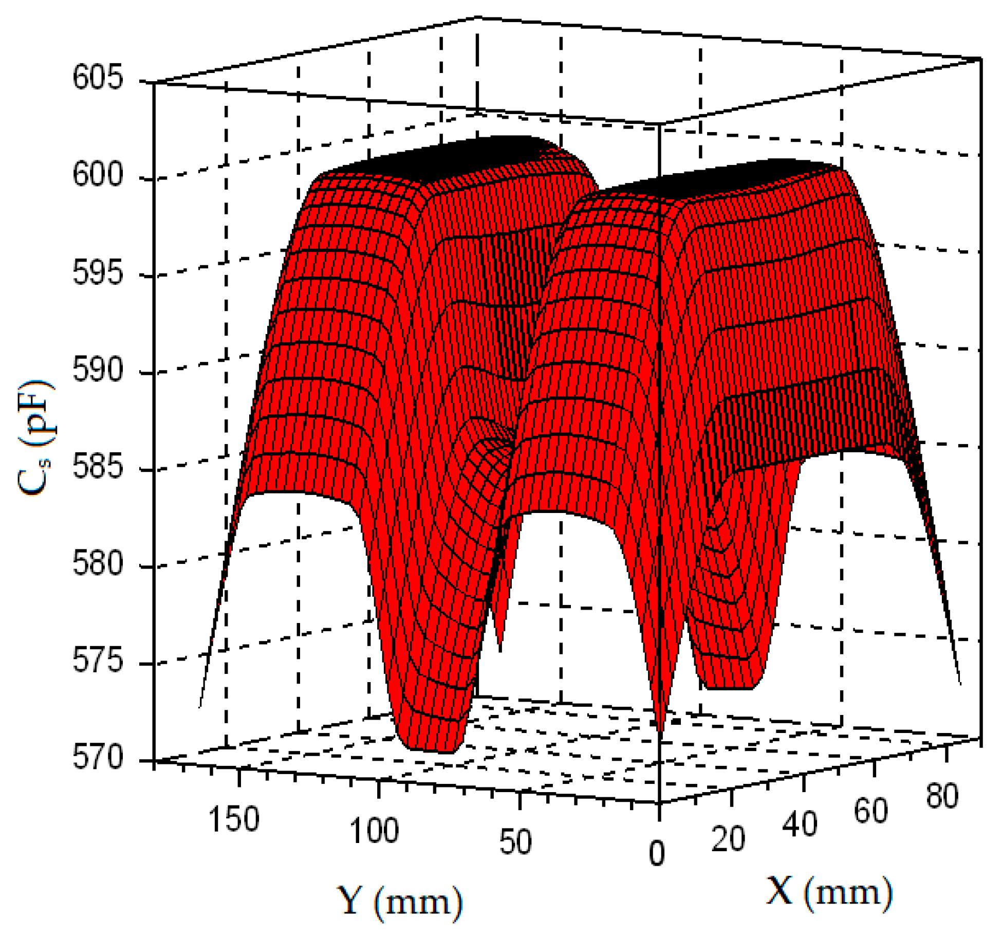
Cs describing the resultant capacitance of the transmitting system has been shown in
Figure 8.
The relationship presented in
Figure 8 shows that the highest values of the resultant capacity
Cs are obtained for positions where the center of the receiving system board is located at a distance corresponding to approximately 1/4 of the length of the transmitter from the outer borders in the
y direction for the adopted reference system and half of the length of the plate in the
x direction of the reference system.
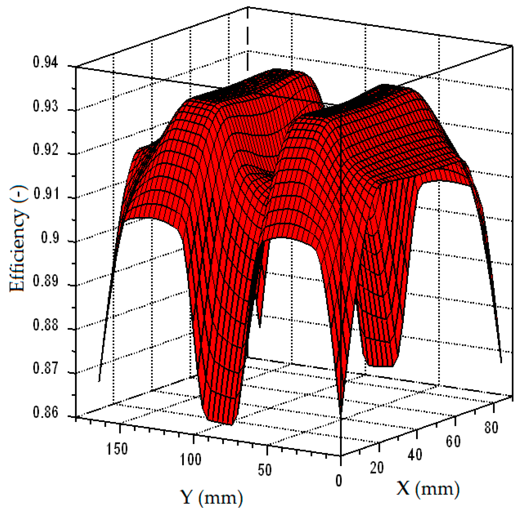
In the next step of studies, the analysis of operating states of the CPT system co-working with an E-class inverter has been performed. The results in form of 3D plots of transmitted power and transmission efficiency have been shown in
Figure 9 and
Figure 10. The calculation of the transmitted power
PT, the input electrical power
Pd supplied to the CPT system and total efficiency
ηt as a function of receiver position have been calculated using the formulas:
Changes in the values of transmitted power and transmission efficiency result directly from fluctuation in the values of individual system capacitances. It can be seen that decreases in efficiency of the CPT system (about 2%) are observed for the central location of the receiving board. However, in this position it can be observed that the system obtains the maximum power values that can be transferred between the transmitter and the receiver, obtaining values of 20.5 W. The highest values of the system efficiency, as could be expected, are obtained for the positions of the receiver located at one quarter of the distance from the outer borders of the transmitter for the adopted direction of the reference system.
The last step of the research was to conduct a simulation in order to verify the current and voltage waveforms on individual elements of the power supply circuit from
Figure 4. Simulation has been performed for the optimal working point, located approximately a quarter of the length of the transmitter from the outer borders in
y direction for the adopted reference system and half of the length of the plate in the
x direction of the reference system. Parameters of the system for that point are as follows:
Ro = 31.56 Ω,
Lr = 50 μH,
CT = 1 nF,
Ld = 1.15 mH,
Cg = 511.25 pF,
Cp1 = 89.07 pF and
Cp2 = 14.77 pF. The simulation has been carried out under following conditions: Δ
Id = 20 mA, Q = 10,
Ud = 40 V and
f = 1 MHz.
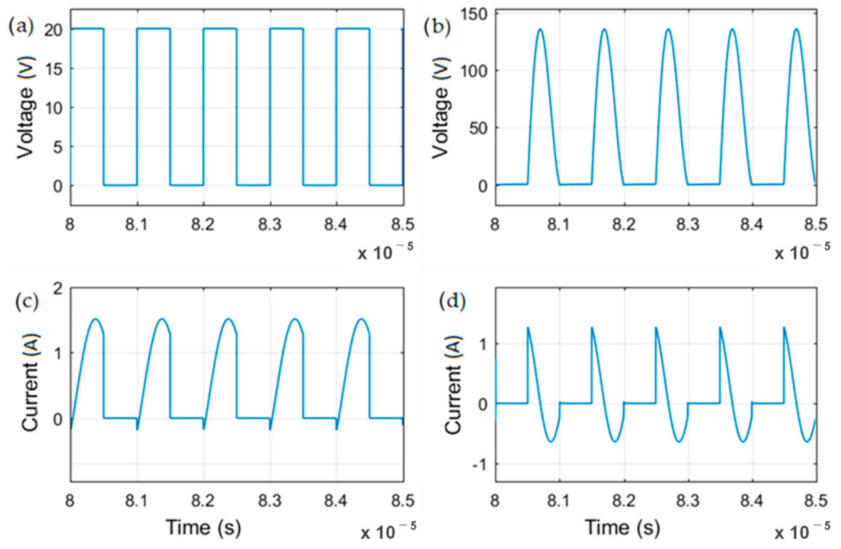
Figure 11,
Figure 12 and
Figure 13 show the current and voltage waveforms corresponded to the elements marked in
Figure 4.
The waveforms in
Figure 11 confirm the validity of performed calculations presented in
Section 4. By analyzing the waveforms of current
IT and voltage
UT on the switching transistor
T1, it can be clearly stated that the system worked in a sub-optimal/near-optimal stage. Due to the fluctuation of circuit parameters related to the change of location of the receiving board, it is impossible to obtain optimal operating conditions for each position of the receiver. However, by maintaining the sub-optimal working conditions in the whole working area, it is possible to obtain high parameters of energy transmission regardless of the fluctuation of the values of individual capacities.
Figure 12 and
Figure 13 present the waveforms of input current
Id and output current (receiver current)
Io, as well as voltage drops on the resonant elements of the system
UL and
UCg respectively. First of all, attention should be paid to the noticeable presence of zero order harmonic in the output current
Io and in the voltage waveforms
UL and
UCg This phenomenon is characteristic of systems supplied by E-class inverters, due to the necessity of separating two resonance systems of different parameters depending on the state of the transistor’s operation.
In order to verify simulation results, the experimental stand of elaborated CPT system was set up and appropriate measurements were conducted. The laboratory stand is shown in
Figure 14. The values of parameters of individual elements that have been used in the laboratory system as well as the position of the receiving plate relative to the transmitting one are corresponded to ones used in the simulation. During tests, values of voltage and current on individual elements of the system have been measured and summarized in the form of waveforms shown in
Figure 15 and
Figure 16.
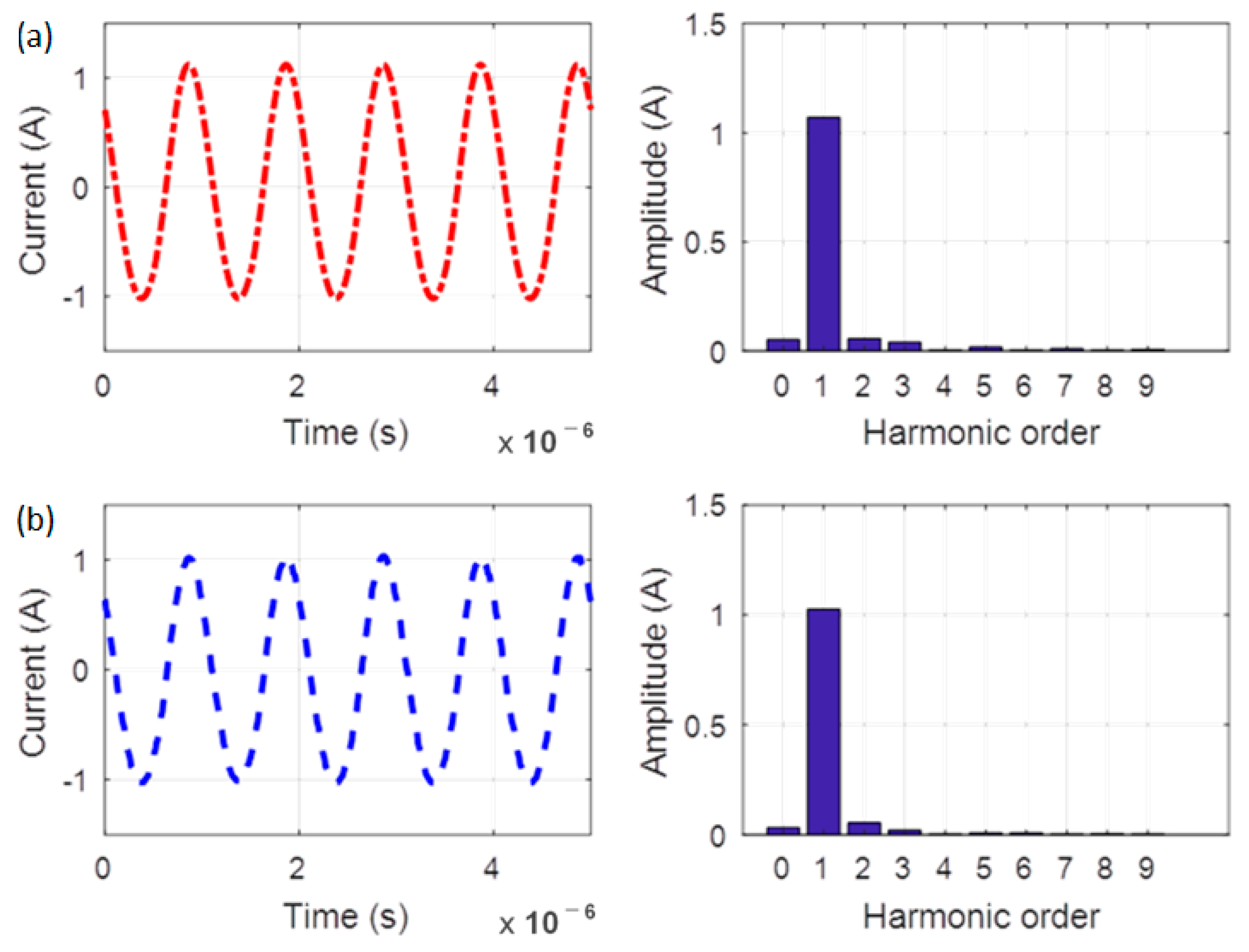
The quality of the obtained waveforms was verified by means of Fast. Fourier Transform (FFT) analysis. The obtained results are presented in
Figure 17. By analyzing the results presented in
Figure 15, it can be noticed that in the receiver current, apart from the first harmonic, the influence of the zero and second harmonic can be also observed. The presence of these harmonics is directly related to the change in configuration of the resonant circuit resulting from the change of operation states of the transistor [
22].
Analyzing the waveforms presented in
Figure 15,
Figure 16 and
Figure 17, the convergence between the results obtained on the basis of the computed simulation and the ones obtained from measurements of the system can be clearly noticed. Undoubtedly, it proves the validity of the assumptions made and the reliability of the elaborated model. However, it should be noted, that there are differences between the efficiency value obtained by simulation (ca. 92%) and measurements (ca. 84%) that result from the negligence of values of coupled capacitor series resistances ESR in simulation process. Therefore, it can be stated that the ESR resistance of the coupled capacitor contributes to a significant decrease in the transmission efficiency. During the tests some observations were made. Both pressure and equilibrium of the receiving plate (i.e., its distribution) is particularly important and have significant impact on operation of the system. Uneven distribution of the receiving plate contributes to the fluctuation of the coupled capacitance value due to formation of the irregular air gap between the transmitting and receiving plates.


