Article

Novel CNN-Based AP2D-Net Accelerator: An Area and Power Efficient Solution for Real-Time Applications on Mobile FPGA

1
VLSI Design and Automation Laboratory, Illinois Institute of Technology, Chicago, IL 60616, USA
2
Department of Computer Science, Rice University, Houston, TX 77005, USA
3
Department of Electrical and Computer Engineering, University of Illinois at Chicago, Chicago, IL 60607, USA
*
Author to whom correspondence should be addressed.
Electronics 2020, 9(5), 832; https://doi.org/10.3390/electronics9050832
Submission received: 22 April 2020 / Revised: 9 May 2020 / Accepted: 12 May 2020 / Published: 18 May 2020
(This article belongs to the Special Issue Advanced AI Hardware Designs Based on FPGAs)

Abstract

:
Standard convolutional neural networks (CNNs) have large amounts of data redundancy, and the same accuracy can be obtained even in lower bit weights instead of floating-point representation. Most CNNs have to be developed and executed on high-end GPU-based workstations, for which it is hard to transplant the existing implementations onto portable edge FPGAs because of the limitation of on-chip block memory storage size and battery capacity. In this paper, we present adaptive pointwise convolution and 2D convolution joint network (AP2D-Net), an ultra-low power and relatively high throughput system combined with dynamic precision weights and activation. Our system has high performance, and we make a trade-off between accuracy and power efficiency by adopting unmanned aerial vehicle (UAV) object detection scenarios. We evaluate our system on the Zynq UltraScale+ MPSoC Ultra96 mobile FPGA platform. The target board can get the real-time speed of 30 fps under 5.6 W, and the FPGA on-chip power is only 0.6 W. The power efficiency of our system is 2.8× better than the best system design on a Jetson TX2 GPU and 1.9× better than the design on a PYNQ-Z1 SoC FPGA.

1. Introduction

Convolutional neural network (CNN)-based deep learning (DL) algorithms are widely used in autonomous driving, natural language processing, web recommendation systems, etc., which greatly improve the quality of life of modern society. However, for more intricate tasks, the number of CNN model parameters grows exponentially. Usually, it takes the order of giga floating-point operations (GFLOP) to process a single image, which is far beyond the computational ability of the central processing unit (CPU) and hard to process in real-time. To overcome those compute-intensive tasks, researchers leverage the advantages of the graphics processing unit (GPU), such as high bandwidth and thread parallelism. The pioneer GPU chip vendors, such as NVIDIA, are also assisting researchers with a systematic and well-designed programming language: CUDA [1], and the NVIDIA CUDA deep neural network (DNN) library: cuDNN [2]. Thus, the NVIDIA GPU can provide higher computational performance and a user-friendly application programming interface (API). Although the GPU’s benefit in the DNN application is obvious, its drawbacks are also remarkable: (1) high power dissipation (usually larger than 200 W [3]) limits the applications of deep learning in the industry field; (2) high-end equipment dependence, such that some research is stuck with applying deeper networks to achieve higher accuracy. However, research on developing high performance and low power deep neural networks is also blooming. FPGA is one of the top solutions to meet the above requirements. FPGA has a high level of flexibility and low power dissipation. However, the bandwidth and on-chip memory of the FPGA are limited compared with the modern GPU. The design challenges such as low bandwidth and limited cache size make it hard to work in real-time. We have to take such challenges and use the FPGA in an optimized manner, and some pipeline architectures [4,5] and data quantization methods have been used to overcome the bottleneck. Even though some 8 bit or 16 bit quantization data types have been applied in FPGA, it still costs a large memory storage size, and it needs to communicate frequently with the onboard memory (DDR). The binary neural network (BNN) [6,7] has drastically reduced the memory size and simplified the multiply-accumulate operation (MAC) to bitwise operation, which increases the power efficiency potential. Horowitz [8] presented rough power measurements in memory access and arithmetic operations on 45 nm technology. According to Table 1, a smaller memory access size can save more power on on-chip memory, and the power dissipation of DRAM access is orders of magnitude larger than cache access. Table 2 concludes that the fewer bit data operations cost less power. Integer data operations cost less energy than floating-point. The add operations cost less energy than multiply operations. The memory access costs much more energy than arithmetic operations. Compared with 32 bit floating/fixed-point data, BNN can reduce the memory size and memory access by 32 times in theory.
In this paper, we design a CNN-based accelerator based on the binary quantized networks on edge FPGA devices for unmanned aerial vehicle (UAV) object detection. Our design is configurable for different sizes of neural networks and pipelining structures for high throughput. We summarize the factors that affect the performance and power consumption of the mobile FPGA accelerator through different experiments. This paper has the following contributions:
  • We propose a CNN structure named adaptive pointwise (PW) convolution and 2D convolution joint network (AP2D-Net), a dynamic precision activation and binary weights combined with PW convolution and 2D convolution structure, which works on resource-limited mobile platforms (such as Zynq UltraScale+ MPSoC Ultra96 or PYNQ-Z1/Z2). The architecture also can be configured on other FPGA platforms according to different hardware resources to achieve the highest throughput.
  • For feature extraction layers, we simplified the convolution operation by using the XOR gate to remove the multiplication operation. Besides, we use offline preprocessing to combine batch normalization (BN) and scale/bias (SB) operation to optimize the computational kernels.
  • To get high bandwidth, we use the advanced extensible interface (AXI4) protocol to communicate between the programming logic (PL), programming system (PS), and memory. Furthermore, we propose a multi-processing scheme to optimize the heterogeneous system and reduce the latency between PL and PS.
  • We conduct a set of experiments considering the running speed, hardware resources, object detection accuracy, and power consumption to get the best combination. The code for training, inference, and our system demo is available online and is open source [9].
The rest of the paper organized as follows. In Section 2, we introduce the background and related works. Section 3 describes the AP2D-Net modeling design, the hardware system design, and optimization. Section 4 presents the experimental setup and results. Finally, Section 5 concludes this paper.

2. Background and Related Work

2.1. Related Work

In the past few years, there have been many different FPGA designs for CNN accelerators [3,5,10,11,12,13,14,15,16,17,18,19,20,21,22,23,24,25,26,27,28,29,30]. The above designs can be divided into three categories: computational kernels optimization, bandwidth optimization, and optimization of CNN models.

2.1.1. Optimization of the Computational Kernels

There are mainly three convolution algorithms used in CNNs: general matrix multiplication (GEMM), fast Fourier transform (FFT), and Winograd [31]. Cong et al. [10] provided an algorithmic modification to reduce the GEMM computational workload by 22% on average. However, this work only focused on the GEMM part and ignored the bandwidth design on external memory. Zeng et al. [11] used the optimized frequency domain (fast Fourier transform (FFT)) convolution instead of standard convolution to increase the processing speed. However, FFT-based convolution is fast for large convolution kernels, but state-of-the-art CNNs use small kernel sizes such as 3 × 3. In these small filter scenarios, the performance of FFT is very limited. Some works [12,13] have applied Winograd convolution to replace the traditional convolution operation. The Winograd operation can reduce the multiplication operations, but increases add/subtraction operations and needs extra transform time. Since add/subtraction operations are much faster than multiplications, the overall time can be reduced. Aydonat et al. [12] used Winograd transformation to boost the performance on FPGA, which can achieve a peak performance of 1.3 trillion floating-point operations per second (TFLOPS) for some specific operations such as fully-connected (FC) layer. However, in modern DNN applications, especially for object detection, the FC layer has a low working efficiency, which might cause overfitting. Furthermore, this work [12] only evaluated the performance on AlexNet [14], whose DNN structure is primitive. In our optimized GEMM method, we adopted BNN [6,7] and used the XOR operation to replace multiplication to increase the GEMM computational speed.

2.1.2. Bandwidth Optimization to Improve Throughput

Suda et al. [15] used quantized 16 bit fixed-point operation to improve the throughput. However, the throughput was only 117.8 giga operations per second (GOPS), which was still far less than the real-time requirement. Li et al. [16] applied parallel operations on convolution layers and a batch-based computing method on FC layers to process multiple input images in parallel. However, this method is not suitable for video sequence application, which has a temporality input order. Motamedi et al. [17] provided a way to develop a method to get a feasible weight file for FPGA. Nurvitadhi et al. [18] used special I/O between CPU and FPGA to accelerate the detection process. There were some works [17,20] that applied the roofline model to design the trade-off between computing throughput and required memory bandwidth to maximize the utilization of FPGA resources. Still, the performance was only 61.62 giga floating-point operations per second (GFLOPS) in the work of Zhang et al. [20] and 84.2 GFLOPS in the work of Motamedi et al. [17], respectively, which was far less than real-time application. Gokhale et al. [21] proposed a CNN accelerator that could achieve a peak performance of 200 GOPS. The architecture only included three primary modules: convolution, subsampling, and nonlinear functions, which are not suitable for complex tasks. Rahman et al. [25] proposed an input-recycling convolutional array of neurons (ICAN) architecture implemented by using 32 bit fixed-point MAC units, which could achieve 147.82 GOPS throughput on Virtex-7 FPGA. Qiu et al. [26] used a dynamic precision data quantization method and applied singular value decomposition (SVD) to the weight of the matrix of the FC layer to reduce resource consumption. Besides, they proposed a data arrangement method to improve the utilization of external memory bandwidth. However, the frame rate was only 4.45 fps, which was far less than the real-time application. Guo et al. [27] implemented a programmable and flexible CNN accelerator architecture, together with a data quantization strategy and compilation tool, which could obtain 137 GOPS throughput on Zynq XC7Z045. There were some works [24,28] that proposed a quantitative model for mapping CNNs to the FPGA cluster. A multi-FPGA architecture could improve throughput. However, the power dissipation also increased drastically. Guan et al. [29] proposed an end-to-end framework that took TensorFlow-described DNNs as the input, which generated the hardware implementation with register-transfer level-high-level synthesis (RTL-HLS) hybrid templates.

2.1.3. Model Optimization

Recently, Fujii et al. [22] used the pruning technique on the FC layer to reduce 39.8% of the parameters in the FC layers, which only increased the throughput of the FC layers somehow, and it did not help too much to improve the overall throughput. In fact, due to the low efficiency of the FC layer, it has disappeared in most advanced modern CNN models. Hailesellasie et al. [23] implemented a reduced parameter CNN on Xilinx ZYNQ FPGA, but there still existed a large gap between structure optimization and cross-platform transportable. Bai et al. [30] adopted depthwise separable convolution to replace standard convolution for embedded platforms, which could reduce the operations and parameters. Gong et al. [5] proposed an optimal paralleling scheme and a balanced pruning-based method to reduce the redundancy of FC layers, which could obtain 80 GOPS on Zynq Z7020 FPGA.

2.2. Binary Neural Networks

For GPU implementations, most of the data types are in floating numbers. In FPGA implementations, we usually use 8 bit or 16 bit quantization data types. However, the fixed-point data for the on-chip memory storage are still heavy. BNN [6,7] gives a solution to reduce the memory size. An extreme case of BNN is both input feature maps (IFMs) and weights as binary numbers. In this case, the convolution operation in BNN can be replaced by the XNOR operation and popcount. However, this case will introduce a large accuracy drop. Instead, we usually use a bit width larger than 1 bit to represent IFMs or output feature maps (OFMs) to keep an acceptable accuracy. Some BNN solutions also gave a way to train the DNN on FPGA, e.g., DoReFa-Net [32] gave a possible solution to train the neural networks on FPGA based on the quantized data type. However, the intention of quantifying the gradient to reduce the training time would introduce an unacceptable loss of precision. In our solution, we used dynamic precision weights for different layers and dynamic quantized activation precision to get the best combination between accuracy and speed.

2.3. Implementation Methodologies

For most research, the CNN-based FPGA methodologies can be divided into two categories: register-transfer level (RTL) design methodology [33,34] and high-level synthesis (HLS) methodology. RTL refers to the program through hardware description languages (HDL) such as VHDL and Verilog. This method will cost a longer development period and introduce more complexity during the programming, but can make good use of the FPGA resources without any redundancy and has a better sequential logic control at cycle-wise level. HLS refers to the C/System C-like synthesis, including the OpenCL method (for Intel/Xilinx FPGA both) or Vivado HLS (for Xilinx FPGA only). It generates RTL code automatically from C/C++ source code. Most of the deep learning FPGA designs are developed by using an HLS method [12,15,35,36]. This method can accelerate the design period and easily simulate and modify different designs. For Xilinx Vivado HLS, it supplies some advanced HLS tools such as HLS DNN intellectual property (IP), HLS linear algebra, and HLS digital signal processors (DSPs), which makes the design of the CNN FPGA accelerator much easier. Thus, more and more designs are based on Xilinx FPGA.
Even though recent research has achieved prosperous results, most of the designs only work for high-end FPGAs. There are some drawbacks for these kinds of platforms: (1) High price: High-end FPGAs usually have a very high price from thousands to tens of thousandsU.S. dollars. The high price of the FPGA is not suitable for mass production in industrial and civil applications. (2) High power consumption: The power dissipation of high-end FPGA usually costs dozens of Watts when running. The power is relatively lower than traditional GPUs, but it is still not low enough. Some FPGAs without an ARM core have to work with an external central processing unit (CPU) through the PCI-E port, which will introduce even more power consumption. (3) Large size: The geometric size of high-end FPGAs usually is larger than a tablet and inconvenient to carry. The Xilinx Zynq SoC platform changes the development step for FPGA, as each FPGA is connected with an integrated ARM-based programming system (PS) without any external CPU, and the communication between PS and FPGA programming logic (PL) is very convenient. In addition, it supports the PYNQ framework, which is used to design embedded systems using the Python language and libraries. It can control PS/PL and data movement and simplifies memory-mapped IO, GPIO, DMA data movement, and hardware memory allocation.
In this work, we developed the UAV object detection system for real-time, high accuracy, and low power application combined with RTL IPs such as DMA, AXI4-stream, and DSP to design our CNN FPGA accelerator on the Zynq UltraScale+ MPSoC Ultra96 development board. Ultra96 consists of ARM Cortex A53 with 1.5 GHz and ZU3 FPGA. The price of the Ultra96 board is inexpensive (249 U.S. dollars in 2019), and the size is 85 mm × 54 mm (which is smaller than a 4.7 inch smart phone) and portable. The total power consumption (including the standby power and working power) is 6.6 W, and the active power is only 0.6 W, which is less than 1 W. In Section 3, we will introduce the proposed system design.

3. System Design

3.1. Proposed System Architecture and IP Block Design

There are two main challenges involved in the architectural design of CNN accelerators on FPGA: (1) fetch data latency from global memory to FPGA on-chip memory is a bottleneck in the design; (2) hardware resources on FPGA are limited.
To overcome the data communication limitation between FPGA and CPU, we used the advanced extensible interface (AXI) direct memory access (DMA) controller to transfer data streams between FPGA and DDR memory. The input and output streams are the transferred data format used in this design. Using the limited hardware resources on FPGA creates a trade-off between the parallel/pipeline throughput and hardware cost.
We used AXI DMA for high bandwidth direct memory access between the AXI4 memory mapped (MM) and the AXI4-Stream IP interface [37]. The proposed system block design is shown in Figure 1. The system processor or PS has access to AXI DMA through the AXI4-Lite interface for control. The M_AXI_MM2S port (M—master; MM2S—memory mapped to stream) in AXI DMA connects to PS’s S_AXI_HPport (S—slave; HP—high performance), and this allows the AXI DMA to fetch stream data from PS. The M_AXI_S2MM port (S2MM—stream to memory mapped) in AXI DMA connected to PS is used to write the stream data from AXI DMA to PS. The S_AXI_HP0 and S_AXI_HP1 are standard AXI high performance interfaces in PS, which are used for the write and read channels. The prefix S stands for “slave”, which means the PL master can access (no matter read or write) the PS. The AXI DMA is connected through the AXI interconnect in the system.
The AXI DMA block diagram is shown in Figure 2. AXI DMA has two channels: MM2S and S2MM. The high-speed DMA data movement from the memory to stream target is performed through the AXI4 MM read to the AXI4 MM2S master. Whereas, the data movement from the stream target to memory is performed through the AXI4 S2MM slave to AXI4 MM write. A logic controller is used to control the sending of data through MM2S channel to the target IP. The same controller is used to control the receiving of data from the target IP through S2MM channel.
In Section 3.2, Section 3.3 and Section 3.4, we will introduce the modeling of AP2D-Net, the corresponding hardware design on FPGA, and the optimization of the heterogeneous system, respectively.

3.2. AP2D-Net Modeling of the CNN-Based FPGA Accelerator

In order to achieve high accuracy, a standard 2D convolution operation with sufficient number of parameters is performed to extract the features. However, a large number of parameters will also introduce a heavy burden on bandwidth and memory. Therefore, pointwise (PW) convolution is utilized to employ a limited number of parameters on the target device while maintaining high-speed and accuracy requirements. Pointwise convolution is also called 1 × 1 convolution or network in network (NIN) [38], which is used to reduce the dimension of the feature map (FM). In this paper, a combination of pointwise convolution and standard 2D convolution was proposed by concatenating pointwise convolution and standard 2D convolution together and generating a new structure named the P2D structure. In addition, we applied dynamic quantized activation precision in the P2D structure named AP2D-Net. This is discussed as follows.

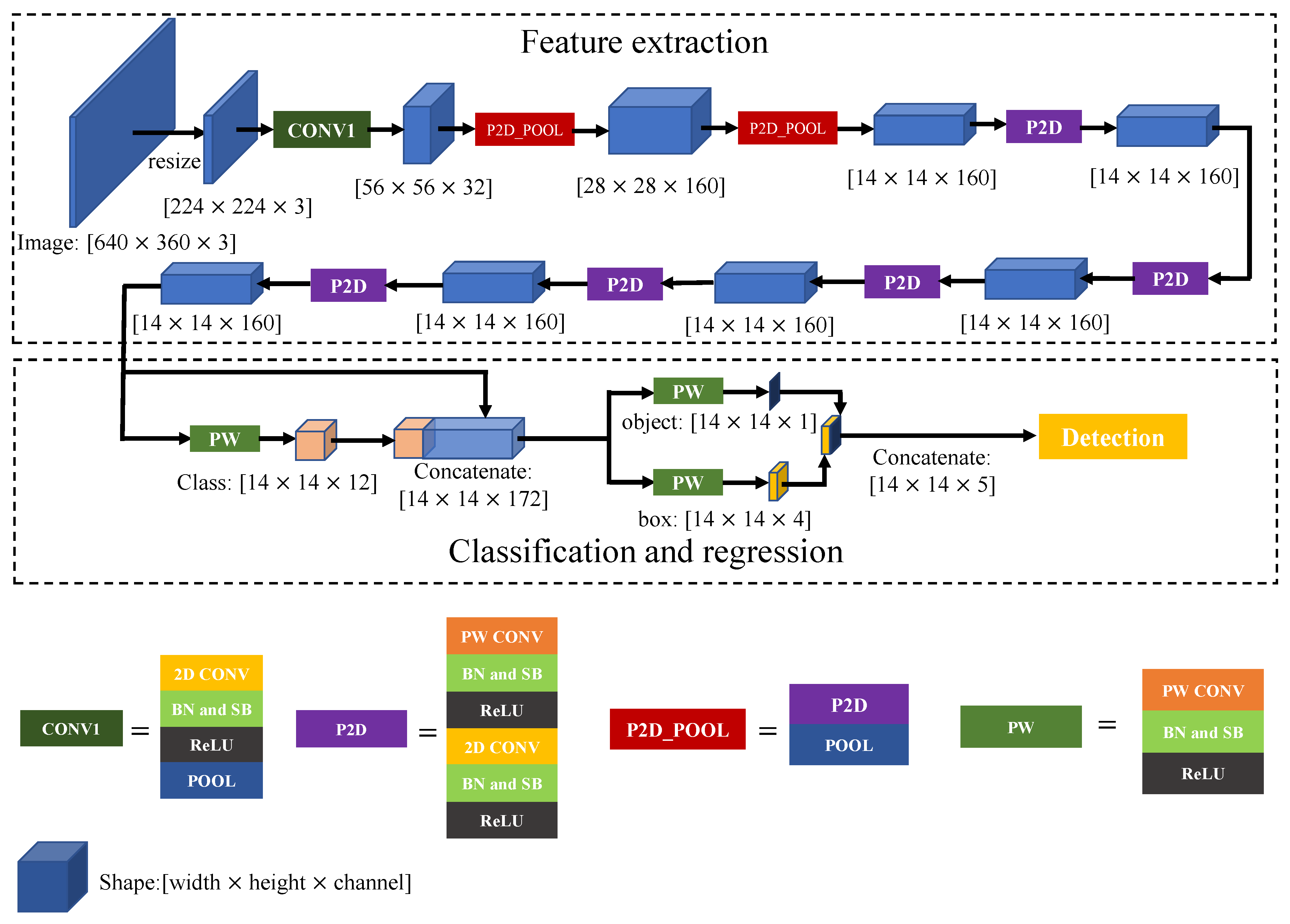
3.2.1. Structure of AP2D-Net

Figure 3 illustrates the structure of AP2D-Net. The model consisted of two parts: the first 15 convolution layers were used to extract the features, and the last three convolution layers were used for object classification and bounding box (BB) regression. The detection module would choose and output the object and location with the highest confidence score. In this model structure, the shape of the input image was 640 × 360 × 3.
The input image stream was resized to 224 × 224 × 3 before sending to PL. Here, we set up the OFM of P2D to have 160 channels, and we will analyze the reason in Section 4.4.

3.2.2. Feature Extraction

For the feature extraction portion, the first convolution layer (CONV1 in Figure 3) is a standard 2D convolution, which includes 2D convolution (CONV), batch normalization (BN), scale/bias (SB), activation (ReLU), and pooling operation. For the next 14 feature extraction layers, the kernels/weights are represented in binary numbers. The standard binarization function is:
x b = s i g n ( n ) = + 1 i f 0 1 o t h e r w i s e
The weights are divided into two categories according to their values being above or below zero. For 1 bit representation on FPGA, we used (2) instead of (1) for the implementation.
x b = s i g n ( n ) = 0 i f 0 1 o t h e r w i s e
For the classification and regression portion, we used 24 bit weights to ensure the final output bounding boxes’ coordination with a high accuracy.

3.2.3. Classification and Regression

Different from ImageNet classification, object detection includes two tasks: classification and regression. Classification gives the class to which the object belongs, and regression gives the information for each object’s coordinate in an image.
For network training, we applied the loss function from the idea of the YOLO framework [39] for object detection. Because the input image resolution was 224 × 224, after downsampling the input size 16 times, the size of the final OFMs was 14 × 14 ( 224 / 16 = 14 ).
The feature extraction part extracted W × H × 5 features, where W and H are the width and height of OFMs in the last layer, respectively. In other words, the image was divided into W × H cells, and for each cell, the feature extractor extracted five features. There were five parameters for each BB: { t x , t y , t w , t h , t o } , and each BB represented by { b x , b y , b w , b h , b o } can be calculated as [39]:
b x = σ ( t x ) + c x b y = σ ( t y ) + c y b w = p w e t w b h = p h e t h b o = σ ( t o )
where { c x , c y } is the top left corner of the cell and { b x / W , b y / H } is the center of BB relative to the whole image. σ ( ) denotes the sigmoid function.
σ ( x ) = 1 1 + e x
{ b w , h h } is the size of BB relative to the bounding box prior { p w , p h } . b o can be expressed as P r ( o b j e c t ) × I O U ( b , o b j e c t ) , where P r ( o b j e c t ) is the confidence of the object and I O U ( b , o b j e c t ) is the intersection over union (IOU) between the predicted BB and ground truth BB.
The loss function can be described as:
l o s s t = λ n o o b j i = 0 W 1 j = 0 H 1 k = 0 B 1 I i j k n o o b j b o i j k 2 + λ o b j i = 0 W 1 j = 0 H 1 k = 0 B 1 I O U ( B B p r e d , B B g t ) I i j k o b j ( 1 b o i j k ) 2 + λ c l a s s i = 0 W 1 j = 0 H 1 I i j o b j c c l a s s e s M S E ( C ) + λ c o o r d i = 0 W 1 j = 0 H 1 k = 0 B 1 ( 2 w g t h g t ) I i j k o b j ( ( b x b x ) 2 + ( b y b y ) 2 + ( t w t w ) 2 + ( t h t h ) 2 )
There are four terms calculated in the loss function: no-object, object, class, and coordinates loss. I i j k n o o b j denotes that the k th BB in location ( i , j ) will be penalized if the IOU is lower than a threshold value T. I i j k o b j denotes that the k th BB in location ( i , j ) is responsible for that prediction. I i j o b j denotes if the object is in location ( i , j ) . I O U ( B B p r e d , B B g t ) is the IOUbetween predicted BBand ground truth BB. MSEloss is used for classification in location ( i , j ) . The last term uses the sum of squared error (SSE) to calculate the coordination loss with the location information. { w g t , h g t } is the ground truth size for BB relative to the whole image. { b x / W , b y / H } is the ground truth of the center coordinate for B B . { t w , t h } is the natural logarithm of the ground truth size relative to the bounding box prior. We define the parameter λ n o o b j = 1 , λ o b j = 5 , λ c l a s s = 1 , λ c o o r d = 1 , and the threshold T = 0.5 .
In this section, we introduced the proposed structure of AP2D-Net. The system design on FPGA will be discussed in Section 3.3.

3.3. AP2D-NET System Design on FPGA

In our AP2D-Net design, we used two convolution operations: standard 2D convolution and PW convolution. Besides convolution operations, in order to get final OFMs, the CNN accelerator had to perform batch normalization (BN), the scale/bias operation (SB), activation (e.g., rectified linearunit (ReLU), etc.), pooling, etc.

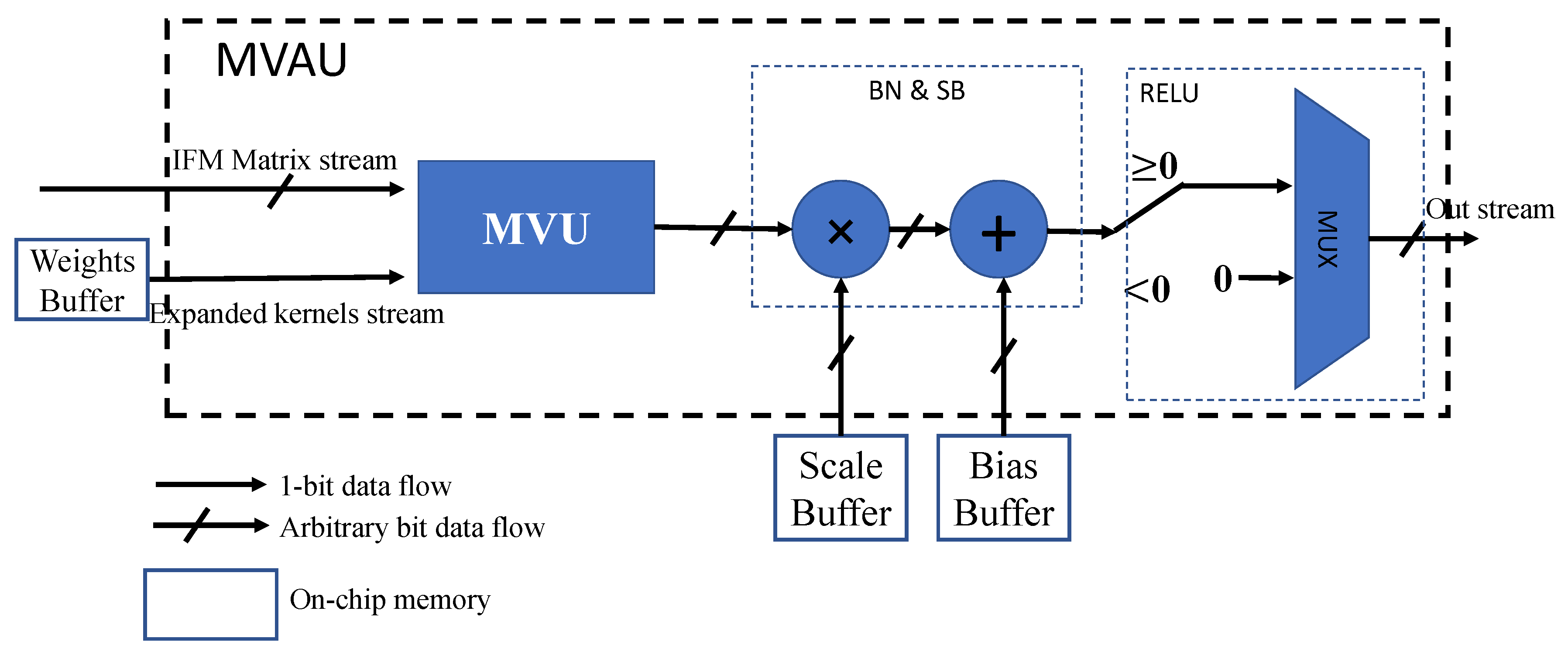
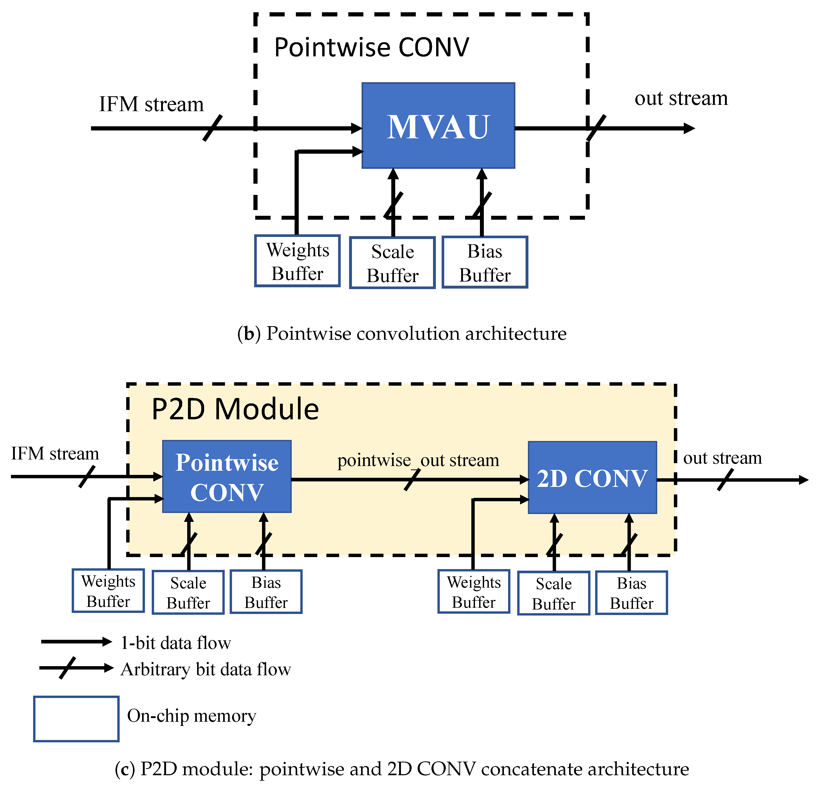
3.3.1. 2D Convolution Module Design

The standard 2D convolution function consisted of two units: sliding window unit (SWU) and matrix vector activation unit (MVAU).

Sliding Window Unit

The SWU was used to convert the IFM into a new matrix for dot production and make the convolution operation faster with the expense of more memory usage. We used a sliding window with a size of D k 2 scanning progressively line-by-line in the IFM. By using the sliding window, the IFM can be expanded to a matrix with M × D k 2 rows and ( D F D k S + 1 ) 2 columns, where S is the stride step. As shown in Figure 4a, the IFM had a shape of 3 × 3 × 2 , and after applying the SWU, the shape of the new matrix ϕ was 8 × 4 . The kernels (or weights) were expanded to row vectors. Since kernels had a 4D shape D K × D K × M × N , we concatenated each 3D cube D K × D K × M into a row vector. Thus, there were N row vectors in total. As shown in Figure 4b, the kernel shape was 2 × 2 × 2 × 2 , and the expanded kernels θ had a shape of 2 × 8 . Since the kernels were generated after training, we could organize and reshape the kernels offline, and there was no time consumption for kernel expansion during inference. In Figure 4c, we applied the dot product between matrix ϕ and kernel θ n , where n denotes the n th row in θ . Thus, there were N times of such a matrix multiplication operation. Finally, we obtained the OFMs with the size of ( D F D k S + 1 ) 2 × N . In this process, we could apply the parallel factor vector_width to reduce the processing time by N v e c t o r _ w i d t h times. In Figure 4c, the shape of final OFMs was 2 × 2 × 2 .

Matrix Vector Activation Unit

The MVAU performs the matrix vector unit (MVU) and then applies the ReLU function for the activation operation.
As shown in Figure 5, the MVU multiplies the expanded kernels θ with the IFM matrix ϕ and generates the OFMs. The time complexity of the MVU operation is:
C M V U o r g = O ( D g · D g · M · N · D k · D k )
In MVU, we applied the parallel factors vector_width and vector_depth. The vectorized factor vector_depth was applied in M IFMs, which helped to reduce the MVU processing time by vector_depth times. The vectorized factor vector_width was applied in N OFMs to generate multiple instances of different kernels. The overall MVU operation could be speeded up by vector_depth× vector_width times.
C M V U n e w = O ( D g · D g · M v e c t o r _ d e p t h · N v e c t o r _ w i d t h · D k · D k )
There was a trade-off between processing capacity and hardware resources or design area. The parallelism parameters vector_width and vector_depth were configured according to the resource usage.
In MVU, ⨁ indicates the XOR operation. Since the weights were binary numbers, the multiply operation could be replaced by adding and subtraction.
θ ϕ = ϕ w h e n θ = 0 ϕ w h e n θ = 1
Let us recall (2): θ = 0 indicates that the binary kernel value is a positive number, while θ = 1 means that the kernel is a negative value. In standard BNN, the positive binary number is represented as +1, and the negative kernel is −1. Thus, we can use XOR to get the correct MAC results in (8).
Batch normalization (BN) allows us to use higher learning rates to speed up the training process and avoids the gradient vanishing problem and gradient exploding problem. It also acts as a regularizer to eliminate the need for dropout [40] and obtains a better detection rate. In the BN layer, we normalized each scalar feature independently. For a layer of d-dimensional input x = ( x ( 1 ) x ( d ) ) , we normalized each dimension:
x ^ ( k ) = x ( k ) E [ X ( K ) ] V a r [ x ( k ) ] + ε
The parameters E [ X ( K ) ] and V a r [ x ( k ) ] are statistically acquired during the training process, and ε is a hyper-parameter. As shown in (9), to calculate a batch normalization operation, it would use two adders (or subtractors), one divider, and one square root operation in hardware. The operation not only costs DSPs and LUTs on FPGA resources, but also increases latency. In addition, the parameters of expectation and variance transferred between external memory and FPGA on-chip memory would introduce a large delay. To solve this problem, we combined batch normalization and scale/bias (SB) operation together.
In the SB layer, we introduced a pair of parameters ( γ ( k ) , β ( k ) ) , which scaled and shifted the normalized value:
y ( k ) = γ ( k ) x ^ ( k ) + β ( k )
We can combine (9) and (10) as:
y ( k ) = γ ( k ) x ( k ) E [ X ( K ) ] V a r [ x ( k ) ] + ε + β ( k ) = x ( k ) { γ ( k ) V a r [ x ( k ) ] + ε } + { β ( k ) E [ X ( K ) ] γ ( k ) V a r [ x ( k ) ] + ε } = x ( k ) Ψ + Ω
where Ψ = γ ( k ) V a r [ x ( k ) ] + ε , Ω = β ( k ) E [ X ( K ) ] γ ( k ) V a r [ x ( k ) ] + ε . Since all of the parameters (such as variance, expectation, scale, and bias) were collected in the training process, we could pre-compute Ψ and Ω offline, which could greatly increase the speed of the CNN FPGA accelerator. In addition, the offline pre-processing could reduce the DSP and LUT resources and arithmetic logic unit (ALU) power consumption during inference.
As shown in Figure 6, the MVAU consisted of three parts: MVU, BN and SB, and ReLU.
  • MVU: This module generated the results after XOR operation between IFMs and kernels. We could apply the parallel mechanism in IFMs and OFMs to reduce the processing time on FPGA.
  • BN and SB: This module would receive the MVU results, multiply them with the pre-compute parameter scale Ψ , and add a parameter bias Ω .
  • ReLU: This module would receive the data after SB and apply the ReLU function in (12).
f ( x ) = x i f 0 0 o t h e r w i s e
After the MVAU, the output stream would be sent out for the next layer’s computation.

2D Convolution and Pointwise Convolution

Figure 7a illustrates the architecture of standard 2D convolution. There were mainly three parts in 2D convolution: padding, SWU, and MVAU, and the padding was optional. For standard 2D convolution without padding, the matrix size of OFM would shrink after each layer, which meant the spatial information at the boundaries would be lost. To preserve low level features, we recommend applying the padding operation before 2D convolution. The size of D k 1 2 zero padding was applied around the border of the IFM. SWU was used to reorganize the IFM according to the sliding window (kernel) size and prepare for faster convolution in MVAU, and MVAU output the OFM stream. Figure 7b is the structure of pointwise convolution. The 1 × 1 convolution would not affect the matrix size of OFM. Thus, padding was eliminated. Furthermore, there was no need for SWU to reorganize the IFM. Finally, pointwise convolution only had the MVAU module. In Figure 7c, we concatenated pointwise convolution and 2D convolution and grouped them as a module called the P2D module.

3.3.2. Overall Architecture of the AP2D-Net Accelerator

Figure 8 illustrates the proposed architecture of the AP2D-Net accelerator. As shown in Figure 8, the processing flow of the AP2D-Net accelerator IP could be divided into four categories:
  • For the first layer, the IFMs would go through four modules {standard 2D CONV, pooling, P2D, pooling} and output the first layer’s OFM stream.
  • For the second layer, the IFMs would go through two modules {P2D, pooling} and output the second layer’s OFM stream.
  • If it was the last layer in the feature extraction portion of AP2D-Net, the IFMs would go through six modules {P2D, PW CONV, concatenate, PW CONV (for object classification), PW CONV (for BB regression), detection} and output the object and bounding boxes’ information.
  • For other layers, the IFMs would only go through the P2D module and output the layer’s OFM stream.
In this design, we used the multiplexer (MUX) and demultiplexer (DEMUX) to switch among the branches according to different layers.
The algorithm of this design is shown in Algorithm 1. The input buffer was used to store the input image (for the first layer) or the IFM stream (for other layers). The output buffer was used to store the object and BB stream (for the last layer) or the OFM stream (for other layers). There were L layers in the feature extraction portion of AP2D-Net. The AP2D-Net accelerator would work in a different manner according to the layer number.
Algorithm 1 Algorithm for AP2D-Net IP design.
Input buffer:    Image stream (first layer)
                       IFM stream (the other layers)
Output buffer:  Object and BB stream (last layer)
                       OFM stream (the other layers)
We assumed there were L layers for features extraction in AP2D-Net. l a y e r { 1 , 2 , , L }
{The accelerator handles the input stream depending on different layer numbers in the feature extraction portion.}
if layer == 1 then
     c o n v 1 _ o u t 2 D _ C O N V ( i m a g e _ s t r e a m , i n p u t _ w e i g h t s )
     p o o l i n g 1 _ o u t P o o l i n g ( c o n v 1 _ o u t )
     P 2 D _ o u t P 2 D ( p o o l i n g 1 _ o u t , b i n a r y _ w e i g h t s )
     p o o l i n g 2 _ o u t P o o l i n g ( P 2 D _ o u t )
     o u t p u t _ s t r e a m p o o l i n g 2 _ o u t
else if layer == 2 then
     P 2 D _ o u t P 2 D ( I F M _ s t r e a m , b i n a r y _ w e i g h t s )
     p o o l i n g 3 _ o u t P o o l i n g ( P 2 D _ o u t )
     o u t p u t _ s t r e a m p o o l i n g 3 _ o u t
else if layer == L then
     P 2 D _ o u t P 2 D ( I F M _ s t r e a m , b i n a r y _ w e i g h t s )
     c o n v _ c l a s s p o i n t w i s e ( P 2 D _ o u t , b i n a r y _ w e i g h t s )
     c l a s s _ o u t c o n c a t ( c o n v _ c l a s s , P 2 D _ o u t )
     c o n v _ o b j p o i n t w i s e ( c l a s s _ o u t , o b j _ w e i g h t s )
     c o n v _ b o x p o i n t w i s e ( c l a s s _ o u t , b o x _ w e i g h t s )
     b b o x O b j e c t S e l e c t ( c o n v _ o b j , c o n v _ b o x )
     o u t p u t _ s t r e a m b b o x
else
     P 2 D _ o u t P 2 D ( I F M _ s t r e a m , b i n a r y _ w e i g h t s )
     o u t p u t _ s t r e a m P 2 D _ o u t
end if

3.4. Optimization on a Heterogeneous System

For a heterogeneous system, the framework worked on both PS and PL sides. As shown in Figure 9, the AP2D-Net accelerator engine was working on PL, while the image read/resize, final detected object, and BB coordinates’ calculation were working on PS. For a standard heterogeneous workflow, each engine started when the previous operation fed the output. However, when the PS side was working, there was a sleep mode in PS, which introduced a large latency in the workflow. To solve this problem, we used a multi-processing scheme to fill in the gap in PS when PL was working. Theoretically speaking, the performance between multi-threading and multi-processing were quite similar. The reason we used multi-processing instead of multi-threading depended on the characteristic of the Python Global Interpreter Lock (GIL). GIL is a lock that allows only one thread to hold the control of the Python interpreter, which means even when it is working in a multi-threading architecture with multiple CPU cores, the GIL can execute only one thread at a time. For I/O bound programs, it usually has to spend an amount of time waiting for input/output. The multi-processing approach gets its own Python interpreter and memory space so the tasks can execute in parallel. As depicted in Figure 9a, the total latency is:
l a t e n c y o r g = T r e a d _ P S + T A P 2 D + T w r i t e _ P S
where T r e a d _ P S is the image read/resize time on PS, T A P 2 D is the CNN engine working time on PL, and T w r i t e _ P S is the BB calculation and write time on PS. After applying the multi-processing scheme, the image read/resize operation can work simultaneously when the AP2D engine is working. The optimized average latency is:
l a t e n c y o p t = m a x { T r e a d _ P S , T A P 2 D } + T w r i t e _ P S
The relationship between T r e a d _ P S and T A P 2 D is uncertain and depends on the secure digital (SD) card read speed. For the read speed, it varies from 12.5 MB/s to 985 MB/s. If T r e a d _ P S T A P 2 D , the optimized latency is T r e a d _ P S + T w r i t e _ P S . If T r e a d _ P S < T A P 2 D , the latency is T A P 2 D + T w r i t e _ P S .
The experimental results and performance evaluation are discussed in Section 4.

4. Performance Evaluation and Experimental Results
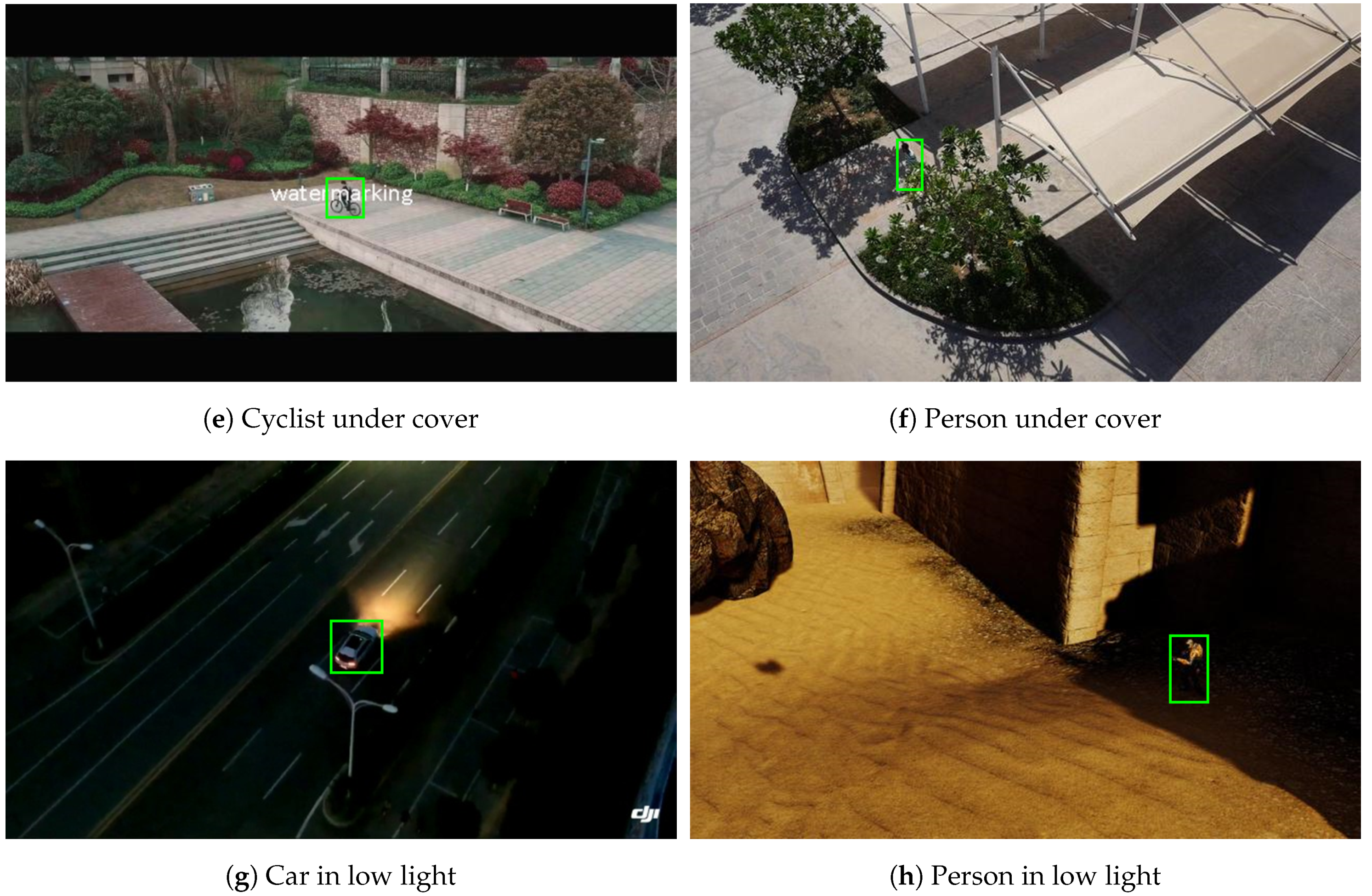
To apply our system on UAV applications, we needed to train the UAV dataset [9] on our AP2D-Net framework to get the weight file.

4.1. Dataset

The dataset [9] had 12 categories for UAV application. As shown in Figure 10, there were several challenges in the dataset. (1) Since it was in a UAV scenario, most of the object that needed to be detected only took a tiny portion (1–2%) in the whole image with the size of 640 × 360 (as shown in Figure 10a,b). The detection accuracy was very sensitive for such a small size. (2) The detection task only focused on a specific object if there were multiple objects, e.g., in Figure 10c, there is a group of people in the captured image, but only one specific object needs to be detected and localized. In Figure 10d, only a specific cyclist needs to be detected. (3) There were obstacles in the images, e.g., the cyclist in Figure 10e is covered by the caption, the person in Figure 10f is partially covered by the tree, etc. (4) The lighting was different. As shown in Figure 10g,h, the scenarios were captured in a low light case.

4.2. Training

To train binary weights during back propagation, we only binarized the weights. The gradients were still real values (floating-point numbers) because the changes of gradients were very tiny. The training would not be successful if we also binarized the gradients. After updating the trained weights, the new value could be binarized since the forward process only needed binary weights.
Before training the dataset, we used some training enhancement methods such as Zhang et al.’s [41], which used visually coherent image mix-up methods for the object detection task. The mix-up method would increase the generalization of the training result. In addition, the distribution of the dataset was unbalanced (as shown in Table 3). The categories “person” and “car” took up more than 20%, while the other categories only took a small portion. To solve the unbalanced distribution, we added data by copying the dataset whose distribution was below 10% to make the dataset more balanced.

4.3. Evaluation Criteria

Bounding box evaluation: For the object detection task, intersection over union (IOU) is an evaluation metric to measure bounding boxes overlap. To measure the detection accuracy, the area of overlap a 0 between the predicted bounding box B p and ground truth bounding box B g t is calculated by (15):
a 0 = a r e a ( B p B g t ) a r e a ( B p B g t )
B p B g t denotes the intersection of the predicted and ground truth BB, and B p B g t is the union of predicted and ground truth BB.
Suppose there are K evaluation images in the dataset; I O U k is the IOU score for the k th image. The average IOU is calculated by:
R I O U = k = 0 K I O U k K
The energy consumption is computed by:
E = P × t
If we know the unit power costs on the FPGA and total time spent during inference, we can get the total energy. Here, E is a criterion considering both the power and speed. Obviously, E should be as low as possible. We assumed E ¯ to be the average energy consumption of the different FPGA accelerator designs. The energy consumption score ES is calculated by:
E S = m a x { 0 , 1 + 0.2 × l o g 2 E ¯ E }
According to (18), we know that if the energy consumption of our design is lower than E ¯ , l o g 2 E ¯ E will be a positive number, which will increase the ES value. On the contrary, if the design costs too much power consumption, it will have a negative effect on ES. The final evaluation score TS is:
T S = R I O U × ( 1 + E S )
In (19), TS combines the accuracy, speed, and power together and gives an overall evaluation.

4.4. AP2D-Net Modeling

There was a trade-off between the accuracy and modeling parameters. To get the best combination, we conducted a set of experiments with dynamic quantized activation precision and other different modeling parameters such as networks channel size and layer number. The optional data realignment engine for an AXI DMA stream data width was up to 512 bit. To guarantee the stream would not excess 512 bit, the model followed the constraint in (20):
A b × C m a x 512
where A b is the activation quantization bit width and C m a x is the maximum channel number in each layer. We list the results in Table 4.
First of all, we set up the activation quantization precision to 5 bit with the same channel numbers, the only difference being the model depth, which was 15, 17, and 19, respectively. According to Table 4, we observed that increasing the model’s depth did not help to increase the accuracy. We analyzed the reason to be that the BNN had only 1 bit representation of weights, and due to the low bit representation, the training of BNN had the gradient vanishing problem. Secondly, we reduced the activation quantization precision from 5 bit to 4, 3, and 2 bit, respectively, and increased the channel numbers of pointwise convolution and 2D convolution gradually. We found that there was a trade-off between the activation quantization precision and the number of channels. Increasing the channel numbers could help to increase the features’ representation ability, which could increase the model’s accuracy. However, reducing the activation quantization precision would also decrease the accuracy. We obtained the summit value when the activation quantization precision was 3 bit with 128 pointwise channels and 160 2D convolution channels. As shown in Figure 11 and Figure 12, the best IOU for training was 0.75 and for validation was 0.55. There are solid lines and ghost lines in Figure 11 and Figure 12. The ghost lines are the original data, which jittered in large amplitude, and it was hard to observe the trends. We used a smoothing factor of 0.6 to make the curve more stable and obtain clear IOU results. In the legend, A/P/D/Lrepresented for activation quantization precision, pointwise channel number, 2D convolution channel number, and layer number, respectively. We used 90,000 images for training, and it took 100k epochs in total.
After getting the model with the highest IOU, we wanted to apply the model in a most power efficient way. The higher speed would increase power consumption. We found that there was a trade-off between the PL working frequency and energy consumption.

4.5. Trade-Off between Working Frequency and Energy Consumption

As shown in Figure 13, we synthesized PL under a range of clock frequency from 125 MHz to 500 MHz (The quad-core ARM Cortex-A53 CPU was running at 1.5 GHz. We used clock divisors 12, 10, 7, 5, 4, and 3 to get the working frequency at 125 MHz, 150 MHz, 214.3 MHz, 300 MHz, 375 MHz, and 500 MHz, respectively. The PS side only supported a frequency up to 333.333 MHz. However, the PL supported synthesis at 500 MHz. Our system could work up to 500 MHz).
From Figure 13, we observe that the power dissipation was linearly increasing when the synthesis frequency changed, which was consistent with (21):
P = α C V 2 f
where α is the activity factor, C is the capacitance, V is the voltage supply, and f is the clock frequency. The power dissipation was increased from 4.8 W to 6.5 W. The speed was also increased from 23.5 fps to 33.7 fps. According to (17), we could compute the energy value at different working frequencies. The energy dissipation could get the minimum value of 0.1831 Joules at 300 MHz when the fps were 30.53 and power was 5.59 W. Thus, we used the frequency at 300 MHz in this design. It is worth mentioning that the power dissipation was the total power dissipation of the Ultra96 board. If we stopped running the program, the standby mode power was 5 W, which meant the active power cost was only 0.59 W.

4.6. Hardware Usage on FPGA

Table 5 lists the hardware usage of our AP2D-Net system on FPGA when we set the parallelism factors v e c t o r _ d e p t h = 32 and v e c t o r _ w i d t h = 8 . Specifically, for the first layer IFMs, v e c t o r _ w i d t h = 3 because the first layer IFMs only had three channels. DSPs are dedicated floating/fixed-point arithmetic operation units such as multiply and accumulators. Block RAMs are a very small embedded memory system on FPGA. LUTs and registers can build and route arbitrary topologies for programmable logic.

4.7. Comparison with FPGA/GPU Designs

We compared our design with the state-of-the-art CNN FPGA accelerator designs listed in Table 6. The work in [5,27] used the FPGA platform Zynq XC7Z020, which has similar hardware resource capacities as our Ultra96 SoC FPGA platform, but they only obtained a throughput of 84.3 GOPS and 80.35 GOPS, respectively. Ma et al. [19] achieved a throughput of 715.9 GOPS on Arria 10 Intel FPGA, which was far above our throughput because the BRAM and DSP size of Arria 10 was 13 × and 5 × larger than our device, respectively. This kind of high-end FPGA collaborating with the external CPU would introduce high power consumption, which would decrease the overall power efficiency. In addition, it is not suitable for mobile applications. The work of Bai et al. [30] implemented MobileNet V2 on Arria 10 SoC, which obtained a throughput of 170.6 GOPS, but the usage of BRAMs and DSPs was far above our device. Geng et al. [24] achieved a throughput of 290 GOPS by using a high-end device that cost 7 × more DSPs, and the power efficiency was 8.28 GOPS/W. The work of Guan et al. [29] could achieve 364.4 GOPS, and the power efficiency was 14.57 GOPS/W.
The power efficiency of our proposed design could reach 23.3 GOPS/W, which outperformed the previous works. It is worth mentioning that the throughput of our design was 130.2 GOPS because the hardware resources were very limited on this mobile FPGA platform. Ultra96 is just a tiny mobile SoC FPGA, and the resource is only 1/5–1/4 compared with the other traditional high-end FPGAs. However, our throughput outperformed the design on comparable devices such as in [5,27].
Table 7 lists the results for the UAV object detection task compared with our proposed AP2D-Net structure based on mobile platforms. ICT-CAS and TGIIF are the most advanced designs on mobile GPU and mobile FPGA, respectively [42]. ICT-CAS uses the YOLO model as the base design structure. It can get an IOU around 0.69 because it uses a high accuracy floating-point inference on GPU and hard example mining training. Due to the limited on-chip memory and bandwidth, the CUDA-based CNN model on GPU is hard to transplant to our mobile FPGA board. The drawback of Jetson TX2 is the high power consumption, which results in the power efficiency of 1.95 fps/W. TGIIF uses an 8 bit quantized data type and closed source Verilog IP. Besides, it prunes and fine-tunes the network to make it have fewer parameters. The IOU of our design was 0.55 because of the accuracy loss in the binary data type. However, our structure could get as fast as 30 fps, and the power efficiency was 5.46 fps/W, which was 2.8× better compared with the Jetson TX2 GPU solution and 1.9× better than the PYNQ-Z1 FPGA design. From the results, our FPGA system design outperformed the most advanced GPU and CPU designs with respect to power efficiency.

5. Conclusions

In this paper, we presented AP2D-Net, an ultra-low power and real-time system design for CNN-based unmanned aerial vehicle applications on the Ultra96 SoC FPGA platform. The system could obtain the real-time speed of 30 fps under 5.6 W, and the active power was only 0.6 W. The power efficiency of our system was 2.8× better than the best system design on Jetson TX2 GPU and 1.9× better than the design on PYNQ-Z1 SoC FPGA. Our system could be applied to the industrial and civil fields such as road object recognition for autonomous vehicles or drones. In the future, more advanced systems will be designed for high accuracy and low power application on SoC FPGA.

Author Contributions

Conceptualization, S.L., K.S. and Y.L.; Data curation, S.L., K.S. and Y.L.; Funding acquisition, K.C.; Methodology, S.L. and K.S.; Supervision, K.C.; Writing—original draft, S.L. and Y.L.; Writing—review and editing, S.L., Y.L. and N.Y. All authors have read and agreed to the published version of the manuscript.

Funding

This work is supported by the Industrial Core Technology Development Program of MOTIE/KEIT, KOREA (#10083639, Development of Camera-based Real-time Artificial Intelligence System for Detecting Driving Environment & Recognizing Objects on Road Simultaneously).

Acknowledgments

We thank our colleagues from KETIand KEITwho provided insight and expertise, which greatly assisted the research and greatly improved the manuscript. We are grateful to Mahmoud Alashi at Illinois Institute of Technology for carefully reading the manuscript and for a number of suggestions on improving the English style.

Conflicts of Interest

The authors declare no conflict of interest.

References

  1. Nvidia. CUDA Toolkit Documentation: Nvidia Developer Zone—CUDA C Programming Guide v8.0; Nvidia: Santa Clara, CA, USA, 2017. [Google Scholar]
  2. Chetlur, S.; Woolley, C.; Vandermersch, P.; Cohen, J.; Tran, J.; Catanzaro, B.; Shelhamer, E. cudnn: Efficient primitives for deep learning. arXiv 2014, arXiv:1410.0759. [Google Scholar]
  3. Li, S.; Luo, Y.; Sun, K.; Choi, K. Heterogeneous system implementation of deep learning neural network for object detection in OpenCL framework. In Proceedings of the 2018 International Conference on Electronics, Information, and Communication (ICEIC), Honolulu, HI, USA, 24–27 January 2018; pp. 1–4. [Google Scholar]
  4. Wang, D.; Xu, K.; Jiang, D. PipeCNN: An OpenCL-based open-source FPGA accelerator for convolution neural networks. In Proceedings of the 2017 International Conference on Field Programmable Technology (ICFPT), Melbourne, VIC, Australia, 11–13 December 2017; pp. 279–282. [Google Scholar]
  5. Gong, L.; Wang, C.; Li, X.; Chen, H.; Zhou, X. MALOC: A fully pipelined fpga accelerator for convolutional neural networks with all layers mapped on chip. IEEE Trans. Comput.-Aided Des. Integr. Circ. Syst. 2018, 37, 2601–2612. [Google Scholar] [CrossRef]
  6. Courbariaux, M.; Hubara, I.; Soudry, D.; El-Yaniv, R.; Bengio, Y. Binarized neural networks: Training deep neural networks with weights and activations constrained to+ 1 or −1. arXiv 2016, arXiv:1602.02830. [Google Scholar]
  7. Rastegari, M.; Ordonez, V.; Redmon, J.; Farhadi, A. XNOR-net: Imagenet classification using binary convolutional neural networks. In European Conference on Computer Vision; Springer: Berlin, Germany, 2016; pp. 525–542. [Google Scholar]
  8. Horowitz, M. Computing’s energy problem (and what we can do about it). In Proceedings of the 2014 IEEE International Solid-State Circuits Conference Digest of Technical Papers (ISSCC), San Francisco, CA, USA, 9–13 February 2014; pp. 10–14. [Google Scholar]
  9. AP2D-Net. 2019. Available online: https://github.com/laski007/AP2D (accessed on 9 May 2020).
  10. Cong, J.; Xiao, B. Minimizing computation in convolutional neural networks. In International Conference on Artificial Neural Networks; Springer: Berlin, Germany, 2014; pp. 281–290. [Google Scholar]
  11. Zeng, H.; Chen, R.; Zhang, C.; Prasanna, V. A framework for generating high throughput CNN implementations on FPGAs. In Proceedings of the 2018 ACM/SIGDA International Symposium on Field-Programmable Gate Arrays, Monterey, CA, USA, 25–27 February 2018; pp. 117–126. [Google Scholar]
  12. Aydonat, U.; O’Connell, S.; Capalija, D.; Ling, A.C.; Chiu, G.R. An opencl™ deep learning accelerator on arria 10. In Proceedings of the 2017 ACM/SIGDA International Symposium on Field-Programmable Gate Arrays, Monterey, CA, USA, 22–24 February 2017; pp. 55–64. [Google Scholar]
  13. DiCecco, R.; Lacey, G.; Vasiljevic, J.; Chow, P.; Taylor, G.; Areibi, S. Caffeinated FPGAs: FPGA framework for convolutional neural networks. In Proceedings of the 2016 International Conference on Field-Programmable Technology (FPT), Monterey, CA, USA, 21–23 February 2016; pp. 265–268. [Google Scholar]
  14. Krizhevsky, A.; Sutskever, I.; Hinton, G.E. Imagenet classification with deep convolutional neural networks. In Proceedings of the Advances in Neural Information Processing Systems, Lake Tahoe, NV, USA, 3–6 December 2012; pp. 1097–1105. [Google Scholar]
  15. Suda, N.; Chandra, V.; Dasika, G.; Mohanty, A.; Ma, Y.; Vrudhula, S.; Seo, J.s.; Cao, Y. Throughput-optimized OpenCL-based FPGA accelerator for large-scale convolutional neural networks. In Proceedings of the 2016 ACM/SIGDA International Symposium on Field-Programmable Gate Arrays, Monterey, CA, USA, 21–23 February 2016; pp. 16–25. [Google Scholar]
  16. Li, H.; Fan, X.; Jiao, L.; Cao, W.; Zhou, X.; Wang, L. A high performance FPGA-based accelerator for large-scale convolutional neural networks. In Proceedings of the 2016 26th International Conference on Field Programmable Logic and Applications (FPL), Lausanne, Switzerland, 26–29 August 2016; pp. 1–9. [Google Scholar]
  17. Motamedi, M.; Gysel, P.; Akella, V.; Ghiasi, S. Design space exploration of FPGA-based deep convolutional neural networks. In Proceedings of the 2016 21st Asia and South Pacific Design Automation Conference (ASP-DAC), Macao, China, 25–28 January 2016; pp. 575–580. [Google Scholar]
  18. Nurvitadhi, E.; Weisz, G.; Wang, Y.; Hurkat, S.; Nguyen, M.; Hoe, J.C.; Martínez, J.F.; Guestrin, C. Graphgen: An fpga framework for vertex-centric graph computation. In Proceedings of the 2014 IEEE 22nd Annual International Symposium on Field-Programmable Custom Computing Machines, Boston, MA, USA, 11–13 May 2014; pp. 25–28. [Google Scholar]
  19. Ma, Y.; Cao, Y.; Vrudhula, S.; Seo, J.S. Optimizing the convolution operation to accelerate deep neural networks on FPGA. IEEE Trans. Very Large Scale Integr. Syst. 2018, 26, 1354–1367. [Google Scholar] [CrossRef]
  20. Zhang, C.; Li, P.; Sun, G.; Guan, Y.; Xiao, B.; Cong, J. Optimizing fpga-based accelerator design for deep convolutional neural networks. In Proceedings of the 2015 ACM/SIGDA International Symposium on Field-Programmable Gate Arrays, Monterey, CA, USA, 22–24 February 2015; pp. 161–170. [Google Scholar]
  21. Gokhale, V.; Jin, J.; Dundar, A.; Martini, B.; Culurciello, E. A 240 g-ops/s mobile coprocessor for deep neural networks. In Proceedings of the IEEE Conference on Computer Vision and Pattern Recognition Workshops, Columbus, OH, USA, 23–28 June 2014; pp. 682–687. [Google Scholar]
  22. Fujii, T.; Sato, S.; Nakahara, H. A threshold neuron pruning for a binarized deep neural network on an FPGA. IEICE Tran. Inf. Syst. 2018, 101, 376–386. [Google Scholar] [CrossRef] [Green Version]
  23. Hailesellasie, M.; Hasan, S.R.; Khalid, F.; Wad, F.A.; Shafique, M. Fpga-based convolutional neural network architecture with reduced parameter requirements. In Proceedings of the 2018 IEEE International Symposium on Circuits and Systems (ISCAS), Florence, Italy, 27–30 May 2018; pp. 1–5. [Google Scholar]
  24. Geng, T.; Wang, T.; Sanaullah, A.; Yang, C.; Patel, R.; Herbordt, M. A framework for acceleration of cnn training on deeply-pipelined fpga clusters with work and weight load balancing. In Proceedings of the 2018 28th International Conference on Field Programmable Logic and Applications (FPL), Dublin, Ireland, 27–31 August 2018; pp. 394–3944. [Google Scholar]
  25. Rahman, A.; Lee, J.; Choi, K. Efficient FPGA acceleration of convolutional neural networks using logical-3D compute array. In Proceedings of the 2016 Design, Automation & Test in Europe Conference & Exhibition (DATE), Dresden, Germany, 14–18 March 2016; pp. 1393–1398. [Google Scholar]
  26. Qiu, J.; Wang, J.; Yao, S.; Guo, K.; Li, B.; Zhou, E.; Yu, J.; Tang, T.; Xu, N.; Song, S.; et al. Going deeper with embedded FPGA platform for convolutional neural network. In Proceedings of the 2016 ACM/SIGDA International Symposium on Field-Programmable Gate Arrays, Monterey, CA, USA, 21–23 February 2016; pp. 26–35. [Google Scholar]
  27. Guo, K.; Sui, L.; Qiu, J.; Yu, J.; Wang, J.; Yao, S.; Han, S.; Wang, Y.; Yang, H. Angel-Eye: A complete design flow for mapping CNN onto embedded FPGA. IEEE Trans. Comput.-Aided Des. Integr. Circ. Syst. 2017, 37, 35–47. [Google Scholar] [CrossRef]
  28. Zhang, C.; Wu, D.; Sun, J.; Sun, G.; Luo, G.; Cong, J. Energy-efficient CNN implementation on a deeply pipelined FPGA cluster. In Proceedings of the 2016 International Symposium on Low Power Electronics and Design, San Francisco, CA, USA, 8–10 August 2016; pp. 326–331. [Google Scholar]
  29. Guan, Y.; Liang, H.; Xu, N.; Wang, W.; Shi, S.; Chen, X.; Sun, G.; Zhang, W.; Cong, J. FP-DNN: An automated framework for mapping deep neural networks onto FPGAs with RTL-HLS hybrid templates. In Proceedings of the 2017 IEEE 25th Annual International Symposium on Field-Programmable Custom Computing Machines (FCCM), Napa, CA, USA, 30 April–2 May 2017; pp. 152–159. [Google Scholar]
  30. Bai, L.; Zhao, Y.; Huang, X. A CNN accelerator on FPGA using depthwise separable convolution. IEEE Trans. Circ. Syst. II Express Briefs 2018, 65, 1415–1419. [Google Scholar] [CrossRef]
  31. Jordà, M.; Valero-Lara, P.; Peña, A.J. Performance Evaluation of cuDNN Convolution Algorithms on NVIDIA Volta GPUs. IEEE Access 2019, 7, 70461–70473. [Google Scholar] [CrossRef]
  32. Zhou, S.; Wu, Y.; Ni, Z.; Zhou, X.; Wen, H.; Zou, Y. Dorefa-net: Training low bitwidth convolutional neural networks with low bitwidth gradients. arXiv 2016, arXiv:1606.06160. [Google Scholar]
  33. Han, S.; Liu, X.; Mao, H.; Pu, J.; Pedram, A.; Horowitz, M.A.; Dally, W.J. EIE: Efficient inference engine on compressed deep neural network. ACM SIGARCH Comput. Arch. News 2016, 44, 243–254. [Google Scholar] [CrossRef]
  34. Motamedi, M.; Gysel, P.; Ghiasi, S. PLACID: A platform for FPGA-based accelerator creation for DCNNs. ACM Trans. Multimed. Comput. Commun. Appl. 2017, 13, 1–21. [Google Scholar] [CrossRef]
  35. Zhang, C.; Sun, G.; Fang, Z.; Zhou, P.; Pan, P.; Cong, J. Caffeine: Toward uniformed representation and acceleration for deep convolutional neural networks. IEEE Trans. Comput.-Aided Des. Integr. Circ. Syst. 2018, 38, 2072–2085. [Google Scholar] [CrossRef]
  36. Umuroglu, Y.; Fraser, N.J.; Gambardella, G.; Blott, M.; Leong, P.; Jahre, M.; Vissers, K. FINN: A framework for fast, scalable binarized neural network inference. In Proceedings of the 2017 ACM/SIGDA International Symposium on Field-Programmable Gate Arrays, Monterey, CA, USA, 22–24 February 2017; pp. 65–74. [Google Scholar]
  37. Xilinx. AXI DMA v7.1 LogiCORE IP Product Guide. In Vivado Design Suite; Xilinx: San Jose, CA, USA, 2019. [Google Scholar]
  38. Lin, M.; Chen, Q.; Yan, S. Network in network. arXiv 2013, arXiv:1312.4400. [Google Scholar]
  39. Redmon, J.; Farhadi, A. YOLO9000: Better, faster, stronger. In Proceedings of the IEEE Conference on Computer Vision and Pattern Recognition, Honolulu, HI, USA, 21–26 July 2017; pp. 7263–7271. [Google Scholar]
  40. Ioffe, S.; Szegedy, C. Batch normalization: Accelerating deep network training by reducing internal covariate shift. arXiv 2015, arXiv:1502.03167. [Google Scholar]
  41. Zhang, Z.; He, T.; Zhang, H.; Zhang, Z.; Xie, J.; Li, M. Bag of freebies for training object detection neural networks. arXiv 2019, arXiv:1902.04103. [Google Scholar]
  42. Xu, X.; Zhang, X.; Yu, B.; Hu, X.S.; Rowen, C.; Hu, J.; Shi, Y. Dac-sdc low power object detection challenge for uav applications. IEEE Trans. Pattern Anal. Mach. Intell. 2019. [Google Scholar] [CrossRef] [PubMed] [Green Version]
Figure 1. System block design. AXI, advanced extensible interface; MM2S, memory mapped to stream; S2MM, stream to memory mapped; PS, programming system; AP2D, adaptive PW convolution and 2D convolution joint network; M, master; S, slave; HP, high performance.
Electronics 09 00832 g001
Figure 2. AXI DMA block diagram. MM, memory mapped.
Electronics 09 00832 g002
Figure 3. AP2D-Net structure for feature extraction, classification, and regression. PW, pointwise; BN, batch normalization; SB, scale/bias.
Electronics 09 00832 g003
Figure 4. Sliding window unit.
Electronics 09 00832 g004
Figure 5. The matrix vector unit (MVU) module.
Electronics 09 00832 g005
Figure 6. Matrix vector activation unit (MVAU) architecture.
Electronics 09 00832 g006
Figure 7. Architecture of 2D CONV and pointwise CONV. SWU, sliding window unit.
Electronics 09 00832 g007aElectronics 09 00832 g007b
Figure 8. AP2D-Net accelerator data flow. bbox, bounding box.
Electronics 09 00832 g008
Figure 9. Optimization scheme on the PS side.
Electronics 09 00832 g009
Figure 10. Dataset examples.
Electronics 09 00832 g010aElectronics 09 00832 g010b
Figure 11. Training IOU for different AP2D-Net models. A, activation quantization precision; P, pointwise convolution channel number; D, 2D convolution channel number; L, layer number.
Electronics 09 00832 g011
Figure 12. Validation IOU for different AP2D-Net models. A, activation quantization precision; P, pointwise convolution channel number; D, 2D convolution channel number; L, layer number.
Electronics 09 00832 g012
Figure 13. Power vs. speed for different working frequencies.
Electronics 09 00832 g013
Table 1. Energy dissipation for memory access.
Memory TypeMemory SizeEnergy Dissipation
Cache (on-chip memory) 64 bit8 KB10 pJ
32 KB20 pJ
1 MB100 pJ
DRAM-1.3–2.6 nJ
Table 2. Energy dissipation for different arithmetic operations.
Data TypeOperationWidth (Bit)Energy Dissipation (pJ)
FloatingAdd160.4
320.9
Multiply161.1
323.7
IntegerAdd80.03
320.1
Multiply80.2
323.1
Table 3. Distribution of the dataset.
CategoryPersonCarRidingBoatGroupWakeboarderDroneTruckParagliderWhaleBuildingHorse Rrider
Percentage (%)29.9026.7418.185.575.153.532.762.541.811.641.440.74
Table 4. IOU vs. different modeling parameters.
Activation QuantizationPW CONV Channel #2D CONV Channel #Feature Extraction Layer #Training IOUValidation IOU
5 bit6496150.650.53
5 bit6496170.640.52
5 bit6496190.650.50
4 bit128128150.650.53
3 bit128160150.750.55
2 bit128256150.720.49
Table 5. Hardware usage on FPGA.
Component (Total)Percentage (%)
LUT (70K)77.6
Flip-flop (F/F) (141K)66.9
DSP (360)79.7
BRAM (216)75.2
Table 6. Comparison among different CNN-based FPGA accelerators.
[5][30][27][24][29][19]Our Work
Year2018201820182018201720182019
CNN modelAlexNetMobileNet V2VGG16VGG16VGG19VGG16AP2D-Net
FPGAZynq XC7Z020Intel Arria 10 SoCZynq XC7Z020Virtex-7 VX690tStratix V GSMD5Intel Arria 10Ultra96
Clock (MHz)200133214150150200300
BRAMs (36Kb)2681844 †85.51220919 †2232 †162
DSPs2181278190216010361518287
LUTs49.8K-29.9K---54.3K
Flip-flop (F/F)61.2K-35.5K---94.3K
Precision (W, A) *(16, 16)(16, 16)(8, 8)(16, 16)(16, 16)(16, 16)(1–24, 3)
Latency (ms)16.73.75364106.6107.743.232.8
Throughput (GOPS)80.35170.684.3290364.4715.9130.2
Power (W)---3525-5.59
Power efficiency (GOPS/W)---8.2814.57-23.3
* W: weight bits; A: activation bits. † Intel FPGA: the size of BRAM refers to 20 Kb.
Table 7. Comparison between mobile FPGA and mobile GPU for UAV object detection.
TGIIF [42]ICT-CAS [42]Our Work
Mobile deviceFPGA PYNQ-Z1GPU Jetson TX2FPGA Ultra96
IOU0.620.690.55
Speed (fps)11.9524.5530.53
Power (W)4.212.585.59
Power efficiency (fps/W)2.851.955.46

