Abstract
This paper presents a sub-threshold differential CMOS Schmitt trigger with tunable hysteresis, which can be used to enhance the noise immunity of low-power electronic systems. By exploiting the body bias technique to the positive feedback transistors, the hysteresis of the proposed Schmitt trigger is generated, and it can be adjusted by the applied bias voltage to the bulk terminal of the utilized PMOS transistors. The principle of operation and the main formulas of the proposed circuit are discussed. The circuit is designed in a 0.18-μm standard CMOS process with a 0.6 V power supply. Post-layout simulation results show that the hysteresis width of the Schmitt trigger can be adjusted from 45.5 mV to 162 mV where the ratio of the hysteresis width variation to supply voltage is 19.4%. This circuit consumes 10.52 × 7.91 μm2 of silicon area, and its power consumption is only 1.38 µW, which makes it a suitable candidate for low-power applications such as portable electronic, biomedical, and bio-implantable systems.
1. Introduction
As the electronics world is heading toward the future, electronic devices require longer lifetime batteries. Hence, the IC designers are obliged to make use of some design techniques to provide a prolonged battery life. One of the common techniques is reducing the supply voltage to decrease the power consumption of the circuits by operating transistors in the weak inversion region. At low voltage, one of the main constraints faced is the device noise level. The weak inversion region is also known as the sub-threshold region because it occurs under the threshold voltage of transistors where very small currents can be provided. The current-voltage equation in this region is an exponential relationship, and although for a given power budget, the gm/ID ratio is at its maximum level; since the values of currents are so small, the circuit may become sensitive to noise [1,2]. Moreover, circuits which operate in the sub-threshold region face some limitations such as poor frequency response and poor linearity [2]. Thus, in general, these circuits are meant for low-frequency and low-current applications such as biomedical and biotelemetry devices and are not suitable for medium power applications [3,4].
A valuable solution to improve the robustness of the circuits to noise is using Schmitt triggers. Schmitt triggers can improve the sensitivity of electronic systems to electromagnetic interferences, i.e., they increase the static noise margin of the circuits but at the cost of more power consumption and delay [5,6]. Accordingly, in general, it is expected that the circuits based on Schmitt triggers operate more reliably in terms of noise immunity [7]. The Schmitt trigger is a bi-stable circuit that is utilized in both analog and digital signal processing systems [8]. The reason for the popularity of this circuit is its hysteresis characteristic or its ability to work in two different threshold levels, which enables the Schmitt trigger to suppress noise in various analog and digital circuits [9]. Indeed, the Schmitt trigger is a restoring signal circuit [10], which eliminates noise content from the input signal and extracts the original input signal information. The positive feedback that causes the circuit loop gain to be more than one is the most popular scheme in creating distinct threshold levels to provide the hysteresis characteristic. The feature that equips the Schmitt trigger with analog to digital conversion and therefore reshapes the pulses can be implemented by either internal or external positive feedback. The positive feedback can be controlled internally or externally according to the intended application and noise tolerance [11,12]. It is worth noting that since different threshold levels can cause different outputs, the hysteresis characteristic might not be desirable in some applications, such as ADC converters [13].
Hysteresis of a Schmitt trigger is directly affected by process variations and transistor mismatches. This issue is more problematic in applications where the level of noise and disturbances is not predictable [8]. To overcome this deficiency, Schmitt triggers with tunable hysteresis can be used as a helpful solution. Besides, the possibility of controlling the hysteresis levels in some applications such as power amplifier circuits [14] leads to lower power consumption and improves the overall performance of the circuit [15].
Generally, traditional single-output Schmitt triggers used to be realized by operational amplifiers and passive components, which had some significant defects such as high-power consumption, limited-gain bandwidth product, low-slew rate, and low-dynamic range. After Allstot, who designed a Schmitt trigger for wireless applications [16], implementing differential Schmitt triggers became widely common. Nowadays, Schmitt triggers, which can convert any periodic signal to its stable logic one, are the fundamental block frequently used in the areas of communication and measurement systems to generate basic waveforms such as square, triangular, pulse, and so on [17,18,19]. Furthermore, relaxation oscillators [20], function generators [21], mono-stable multi-vibrators [22], pulse width modulators [23], and switching power supplies [24] are the other several applications of Schmitt trigger circuits in the emerging areas of signal processing.
In this paper, a differential Schmitt trigger with adjustable hysteresis and transistors that are biased in the sub-threshold region is proposed. Hysteresis of this circuit is created by positive feedback and can be controlled by the body bias technique. In a body driven transistor, the input signal is applied to the bulk terminal to create conduction between the source and drain. Despite the smaller transconductance and bandwidth, this will enhance the application of fundamental analog building blocks in low-voltage environments [2]. In the presented work, by applying the body bias technique to the positive feedback transistors, no additional element is required to equip the circuit with hysteresis control capability. Basically, MOSFETs using the body bias technique are required to have isolated bulk terminals [2], which cause some percent of a larger active area. However, the proposed circuit structure helps to have a Schmitt trigger with fewer transistors and a smaller occupied chip area compared to the recently proposed topologies, which make it suitable for bio-implantable circuits. This paper is organized as follows: The proposed Schmitt trigger is described in Section 2; Section 3 presents the simulation results; finally, the paper is concluded in Section 4.
2. Proposed Schmitt Trigger Circuit Description
2.1. Differential Pair of the Circuit
The differential pair of the proposed low-voltage, low-power Schmitt trigger with tunable hysteresis is illustrated in Figure 1. Transistors of and are the differential inputs, and is a controlled current source that provides the tail current of the differential pair by a bias voltage of . and implement positive feedback to create the hysteresis of the proposed Schmitt trigger.
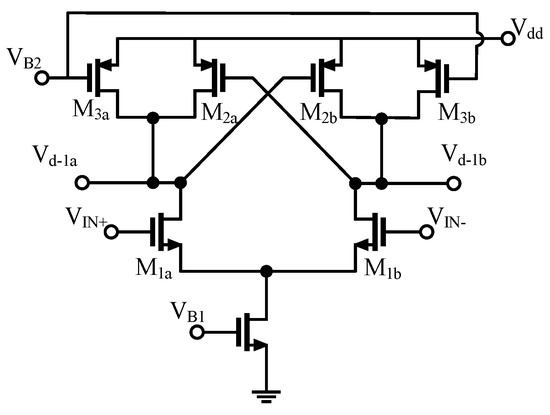
Figure 1.
The differential pair of the proposed Schmitt trigger.
Due to the tail current, when the DC voltage of the positive input, , increases from 0 to positive voltages while is fixed at a mid-point (reference voltage), will be increased, and inversely, will be decreased, which are the drain currents of transistors and , respectively. Thus, based on the differential behavior of the circuit, the drain voltage of decreases and the drain voltage of increases, and switches from high to low in . The DC transfer characteristics of are shown in Figure 2 (gray curve).
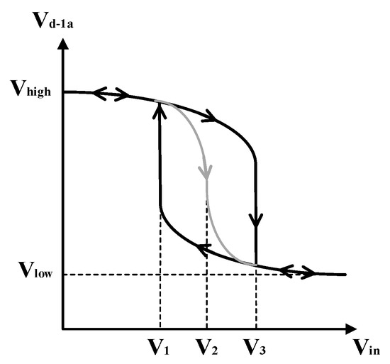
Figure 2.
Qualitative hysteresis characteristic of an inverting Schmitt trigger.
It should be noted that because of , which is a voltage-controlled current source and provides a fixed current, an increase in will increase the drain current of , i.e., . On the other hand, when decreases, reduces as well under the same circumstance. However, the reduction of will force to increase and retain its former situation. Therefore, and accordingly will not change either. Hence, will also retain its former situation, and and will remain unchanged as well. This situation will continue until the difference between and becomes so large that overcomes and the state changes. At this point, will change; its position is denoted as in Figure 2. In contrast, when becomes significantly smaller than , the output current will change its state at the voltage of , which is shown in the figure. This voltage shift from is caused by the positive feedback transistors; and . In the absence of these transistors, the circuit will operate as a comparator. It is perceivable that the proposed Schmitt trigger operates at a current mode, and its operation analysis is described in the following.
According to Figure 1, using KCL at the drain node of the positive input transistor results in:
The drain current equation in the sub-threshold region has an exponential relationship and for a NMOS transistor equals to where . Then, can be approximated as where n and are sub-threshold coefficient and thermal voltage, respectively. Consequently, Equation (1) can be written as:
If we repeat the same path for the drain node of the negative input transistor and subtract from , the voltage difference of input terminals becomes:
2.2. Two-Stage Schmitt Trigger Circuit
In Figure 2, voltage levels of and are LTP and UTP of the Schmitt trigger, respectively. As can be seen, the hysteresis curve will not reach to logical zero or one, which is because of the low gain of the circuit. To solve this problem, an output stage is added to the structure illustrated in Figure 3. After amplifying the signal by the second stage, the hysteresis characteristic will be consistent with Figure 4. In other words, immediately after ’s decrease, the drain current of will also reduce. Then, because of the current mirror of and higher current of , will approach zero and a sharper transition will occur, as depicted in Figure 4.
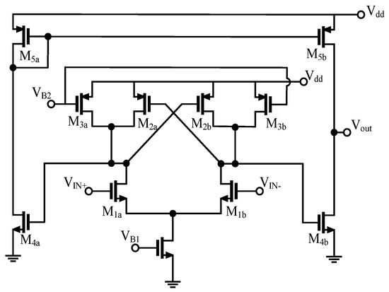
Figure 3.
The proposed two-stage Schmitt trigger.
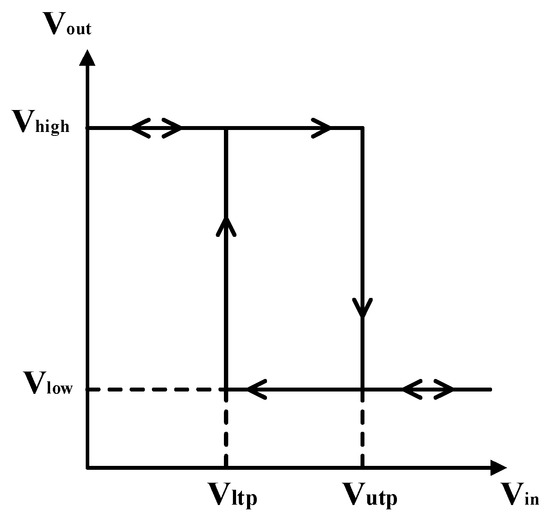
Figure 4.
Qualitative hysteresis characteristic of the two-stage Schmitt trigger.
A KVL from to the source terminal of will result in . Afterward, we can write:
In the following, because of a reduction in the drain voltage of , the current of and subsequently the currents of will decrease. On the other hand, increasing the drain voltage of will increase .
It is clear that the output current is the difference between and . Now, by considering , we will have . After utilizing the sub-threshold drain current equation for transistors , the following equation will be obtained:
Substituting Equation (5) in Equation (4) and then in Equation (3) will yield:
According to the former explanations, when the DC voltage of the positive input increases, the output current decreases, and the output voltage level approaches zero. In contrast, when goes from positive voltages to negative voltages, increases, and changes to the logic one.
2.3. Proposed Structure of the Two-Stage Schmitt Trigger with Adjustable Hysteresis
The proposed low-voltage, low-power differential Schmitt trigger with tunable hysteresis is illustrated in Figure 5. Hysteresis characteristic of this circuit can be controlled by the bulk terminal of the positive feedback transistors . Despite similar works reported in [15,25], no additional transistors are needed to equip the Schmitt trigger with controllable hysteresis. According to Equation (6), when the threshold voltages of change, the hysteresis width of the circuit will also change. Hence, by applying the body bias technique to the positive feedback transistors, an adjustable hysteresis will result.
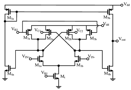
Figure 5.
The proposed Schmitt trigger with adjustable hysteresis.
By exploiting the body bias technique and using the equation, which is , Equation (6) will be changed to:
where and are the body-effect coefficient and surface potential, respectively. Equation (7) declares that by variation of and (bulk terminals of ), hysteresis width can be tuned. It should be noted that must be smaller than . Since the proposed circuit has a 0.6 V supply voltage, the value of cannot exceed mathematically. To avoid leakage current, it is important to consider that cannot be smaller than the supply voltage, and the corresponding voltage levels must be chosen optimally.
3. Post-Layout Simulation Results
The proposed sub-threshold differential Schmitt trigger with tunable hysteresis is designed and post-layout simulated in a standard 0.18 μm CMOS technology. The utilized technology allows bulk and body contacts to be different in the wafer fabrication process. Power consumption of the circuit is 1.38 µW, which makes it suitable for biomedical applications. The layout of the proposed Schmitt trigger is shown in Figure 6, which occupies the chip area of 10.52 × 7.91 μm2. The aspect ratios of transistors are set according to Table 1.
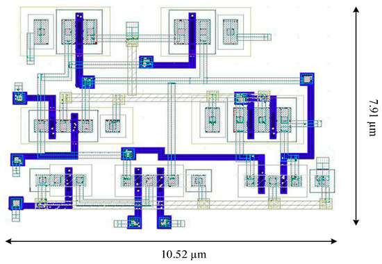
Figure 6.
The layout of the proposed Schmitt trigger in 0.18 μm CMOS technology.

Table 1.
Aspect ratios of the transistors.
The DC voltage transfer characteristic of the proposed Schmitt trigger is shown in Figure 7 where is initially swept from 0 to 0.6 V and then from 0.6 V to 0 to observe the hysteresis curve, while is fixed at 0.3 V. The UTP and LTP of the circuit are 380.1 mV and 254.1 mV, respectively, so the hysteresis width is 126 mV. A triangular waveform with the amplitude of 0.6 V and 500 kHz frequency is applied to , and its corresponding transient output is illustrated in Figure 8.
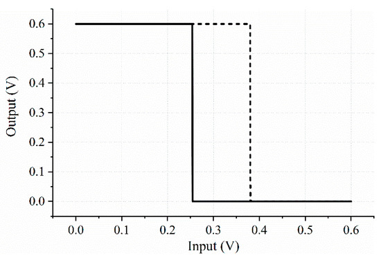
Figure 7.
Voltage transfer characteristics of the proposed Schmitt trigger. Vin+ is swept from 0 to 0.6 V and vice versa, while Vin− is set to 0.3 V, and VB1 and VB2 are 0.35 V and 0.3 V, respectively.
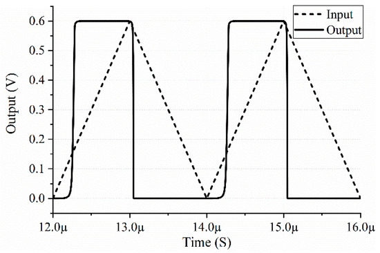
Figure 8.
Time-domain response of the designed Schmitt trigger circuit to 500 kHz triangular input signal.
Figure 9 shows the hysteresis characteristic of the proposed Schmitt trigger while is swept from 0.3 V to 0.6 V. It is clear that the hysteresis width can be varied in proportion to the bias voltage applied to the bulk terminal of the positive feedback transistors M2a and . Moreover, the variation of the transient response of the circuit according to the changes of the body bias voltage, i.e., , is depicted in Figure 10. The voltage transfer characteristic of the proposed Schmitt trigger over different process corners at 27 °C is shown in Figure 11. Variations of the hysteresis width and the center of the circuit in three process corners over temperatures from −20 °C to 60 °C is simulated, and the result is illustrated in Figure 12a,b, respectively.
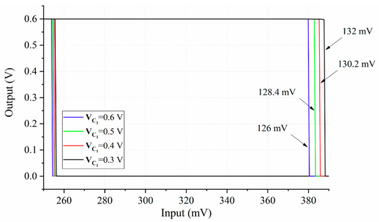
Figure 9.
Dependence of the threshold voltages on the Vc1 variation. Vin+ is swept from 0 to 0.6 V and vice versa, while Vin− is set to 0.3 V.
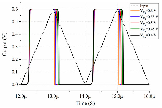
Figure 10.
Variation of the time-domain response of the proposed circuit by changes of Vc1.
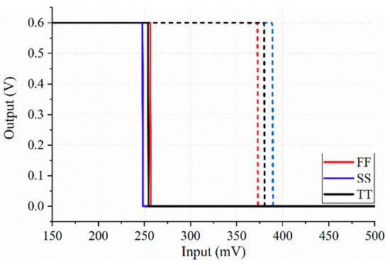
Figure 11.
Variation of the hysteresis width in different process corners at 27 degrees Celsius.
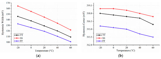
Figure 12.
Variation of hysteresis (a) width and (b) center of the proposed Schmitt trigger from −20 to 60 degrees Celsius in different process corners.
Figure 13 shows the variation of the hysteresis width and its center versus the reference voltage for a constant value of control voltage. In addition to the hysteresis width variation of the circuit by changing Vc1, the width and the center of its hysteresis vary through sweeping Vin− from 250 mV to 450 mV. Figure 14 provides a more comprehensive review of the dependency of the hysteresis width on the control voltage and the reference voltage. It shows that by sweeping Vc1 from 400 mV to 600 mV and simultaneously changing Vin− from 250 mV to 350 mV, hysteresis width changes in a range of 116 mV.
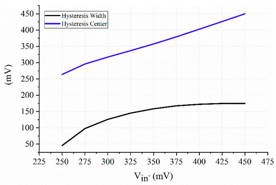
Figure 13.
Variation of the hysteresis width and its center versus reference voltage of Vin− while VC1 is set to 300 mV.
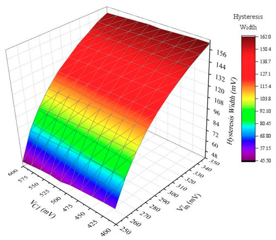
Figure 14.
Dependence of the hysteresis width on the control voltage (VC1) and the reference voltage (Vin−).
To examine the effect of process variations and component mismatches on the transient response of the proposed Schmitt trigger, 100 runs of Monte Carlo analysis are performed for all employed transistors. Figure 15 shows the transient responses of input and output voltages for post-layout simulation of Monte Carlo analysis. Finally, in Figure 16a,b, post-layout simulated histograms for 100 runs of Monte Carlo for LTP and UTP of the circuit are presented. As can be seen, the majority of the iterations for LTP and UTP fit in about 254 mV ± 11% and 380 mV ± 15%, respectively. Moreover, the proposed circuit was simulated with ±10% variation in power supply, for which proper operation was observed (Figure 17).
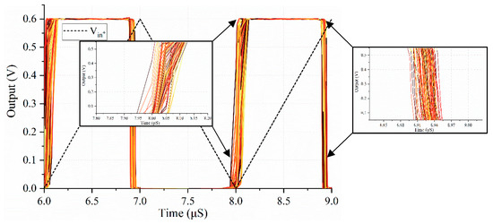
Figure 15.
Post-layout simulation for 100 runs of Monte Carlo on the transient response of the input and output voltages.
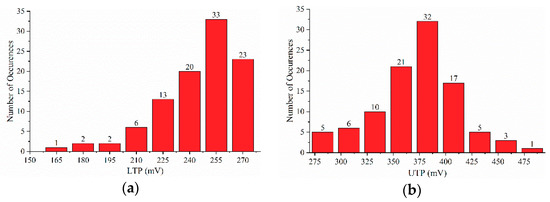
Figure 16.
Post-layout simulated histogram for 100 runs of Monte Carlo for (a) LTP and (b) UTP.
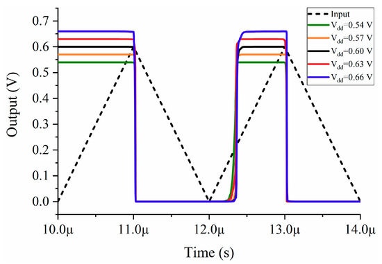
Figure 17.
Transient response of the output voltage with ±10% on the power supply for a triangular saw-tooth input voltage.
Table 2 illustrates the comparison of the proposed and the recent CMOS Schmitt triggers which have almost common properties. The comparison is mainly considered in terms of supply voltage, single or differential input, voltage or current mode, static power consumption, occupied chip area, and hysteresis width. The proposed current mode CMOS Schmitt trigger operates at a voltage supply of 0.6 V and its transistors are biased in the sub-threshold region. Therefore, this circuit has significantly lower power consumption and a smaller occupied chip area, which make it suitable for low-voltage and low-power applications.
Table 2.
Performance comparison of Schmitt triggers.
4. Conclusions
A low-voltage, low-power differential Schmitt trigger for biomedical applications, which operates at 0.6 V supply voltage and current mode, has been presented in this paper. By applying bias voltages in the range of 0.3 V to 0.6 V to the positive feedback transistors, the hysteresis width of the proposed circuit can be varied from 126 mV to 132 mV, which means that its hysteresis width is adjusted by the body bias technique. Moreover, by changing the control voltage and reference voltage simultaneously, a bigger range of hysteresis width variation from 45.5 mV to 162 mV is achievable. This Schmitt trigger consumes 1.38 µW of static power and occupies 10.52 × 7.91 μm2 of the chip area. Properties of this circuit make it a good candidate for low-voltage and low-power applications such as electronic healthcare devices and implantable microsystems.
Author Contributions
Conceptualization and design, S.R. and A.N.; formal analysis, A.N. and S.R.; software, A.N. and S.R.; investigation, M.H.M. and Y.B.; writing—original draft preparation, S.R.; writing—review and editing, M.N. and S.H.-H.; supervision, P.A. and M.H.M.; funding acquisition, S.H.-H. and M.N. All authors have read and agreed to the published version of the manuscript.
Funding
This research received no external funding.
Conflicts of Interest
The authors declare no conflict of interest.
References
- Sansen, W. Analog Design Essentials; Springer: Dordrecht, The Netherlands, 2006. [Google Scholar]
- Rajput, S.; Jamuar, S. Low Voltage Analog Circuit Design Techniques. IEEE Circuits Syst. Mag. 2002, 2, 24–42. [Google Scholar] [CrossRef]
- Calhoun, B.; Chandrakasan, A. A 256-Kb 65-Nm Sub-Threshold SRAM Design for Ultra-Low-Voltage Operation. IEEE J. Solid-State Circuits 2007, 42, 680–688. [Google Scholar] [CrossRef]
- Lee, H.; Mohammadi, S. A 3GHz Subthreshold CMOS Low Noise Amplifier. In Proceedings of the IEEE Radio Frequency Integrated Circuits (RFIC) Symposium, San Francisco, CA, USA, 10–13 June 2006. [Google Scholar]
- Kulkarni, J.; Roy, K. Ultralow-Voltage Process-Variation-Tolerant Schmitt-Trigger-Based SRAM Design. IEEE Trans. on Very Large Scale Integr. (VLSI) Syst. 2012, 20, 319–332. [Google Scholar] [CrossRef]
- Lotze, N.; Manoli, Y. A 62 mV 0.13 µm CMOS Standard-Cell-Based Design Technique Using Schmitt-Trigger Logic. IEEE J. Solid-State Circuits 2012, 47, 47–60. [Google Scholar] [CrossRef]
- Tache, M.; Ibrahim, W.; Kharbash, F.; Beiu, V. Reliability and Performance of Optimised Schmitt Trigger Gates. J. Eng. 2018, 2018, 735–744. [Google Scholar] [CrossRef]
- Yuan, F. Differential CMOS Schmitt Trigger with Tunable Hysteresis. Analog Integr. Circuits Signal Process. 2009, 62, 245–248. [Google Scholar] [CrossRef]
- Hagiwara, T.; Yamaguchi, K.; Shojiro, A. Threshold voltage deviation in very small MOS transistors due to local impurity fluctuations. In Proceedings of the 1982 Symposium on VLSI Technology. Digest of Technical Papers, Oiso, Japan, 1–3 September 1982; pp. 46–47. [Google Scholar]
- Saxena, A.; Akashe, S. Comparative Analysis of Schmitt Trigger with AVL (AVLG and AVLS) Technique Using Nanoscale CMOS Technology. In Proceedings of the Third International Conference on Advanced Computing and Communication Technologies (ACCT), Rohtak, India, 6–7 April 2013. [Google Scholar]
- Nandhasri, K.; Ngarmnil, J. Hysteresis tunable FGMOS comparator. In Proceedings of the ICSE 2000, 2000 IEEE International Conference on Semiconductor Electronics. Proceedings (Cat. No.00EX425), Guoman Port Dickson Resort, Malaysia, 13–15 November 2000. [Google Scholar]
- Ekekwe, N.; Etienne-Cummings, R. Adaptive Hysteretic Comparator with Op-amp Threshold Level Setting. In Proceedings of the 51st Midwest Symposium on Circuits and Systems, Knoxville, TN, USA, 10–13 August 2008. [Google Scholar]
- Goll, B.; Zimmermann, H. Comparators in Nanometer CMOS Technology; Springer: Berlin, Germany, 2016. [Google Scholar]
- Amiri, P.; Nabavi, A.; Mortazavi, S. Low Distortion CMOS Class-D Amplifier with Double-Band Hysteresis. IEICE Electron. Express 2010, 7, 273–280. [Google Scholar] [CrossRef][Green Version]
- Yuan, F. A High-Speed Differential CMOS Schmitt Trigger with Regenerative Current Feedback and Adjustable Hysteresis. Analog Integr. Circuits Signal Process. 2009, 63, 121–127. [Google Scholar] [CrossRef]
- Allstot, D. A Precision Variable-Supply CMOS Comparator. IEEE J. Solid-State Circuits 1982, 17, 1080–1087. [Google Scholar] [CrossRef]
- Minaei, S.; Yuce, E. A Simple Schmitt Trigger Circuit with Grounded Passive Elements and Its Application to Square/Triangular Wave Generator. Circuits Syst. Signal Process. 2011, 31, 877–888. [Google Scholar] [CrossRef]
- Kumar, A.; Chaturvedi, B. Single Active Element-Based Tunable Square/Triangular Wave Generator with Grounded Passive Components. Circuitssyst. Signal Process. 2017, 36, 3875–3900. [Google Scholar] [CrossRef]
- Chung, W.; Kim, H.; Cha, H.; Kim, H. Triangular/Square-Wave Generator with Independently Controllable Frequency and Amplitude. IEEE Trans. Instrum. Meas. 2005, 54, 105–109. [Google Scholar] [CrossRef]
- Onomi, T. Experimental Demonstration and Performance Estimation of a New Relaxation Oscillator Using a Superconducting Schmitt Trigger Inverter. Phys. Procedia 2016, 81, 141–144. [Google Scholar] [CrossRef]
- Kumar, D.; Khatri, R. Function Generator Using Current Conveyor (CCII). Int. J. Comput. Appl. 2016, 147, 1–4. [Google Scholar] [CrossRef]
- Chien, H.-C.; Lo, Y.-K. Design and Implementation of Monostable Multivibrators Employing Differential Voltage Current Conveyors. Microelectron. J. 2011, 42, 1107–1115. [Google Scholar] [CrossRef]
- Lin, B. Phase-Shift PWM Converter with Wide Voltage Operation Capability. Electronics 2019, 9, 47. [Google Scholar] [CrossRef]
- Newsom, R.; Dillard, W.; Nelms, R. Digital Power-Factor Correction for a Capacitor-Charging Power Supply. IEEE Trans. Ind. Electron. 2002, 49, 1146–1153. [Google Scholar] [CrossRef]
- Nejati, A.; Bastan, Y.; Amiri, P.; Maghami, M. A Low-Voltage Bulk-Driven Differential CMOS Schmitt Trigger with Tunable Hysteresis. J. Circuitssystems Comput. 2019, 28, 1–14. [Google Scholar] [CrossRef]
- Park, S.; Kim, K.; Huynh, H.A.; Joo, S.; Kim, S. EM Noise Immunity Enhancement Using Schmitt Trigger Logic Gates in CMOS Process. In Proceedings of the URSI Asia-Pacific Radio Science Conference (URSI AP-RASC), Seoul, Korea, 21–25 August 2016. [Google Scholar]
- Nejati, A.; Bastan, Y.; Amiri, P. 0.4 V Ultra-Low Voltage Differential CMOS Schmitt Trigger. In Proceedings of the Iranian Conference on Electrical Engineering (ICEE), Tehran, Iran, 2–4 May 2017. [Google Scholar]
- Melek, L.A.P.; Silva, A.L.D.; Schneider, M.C.; Galup-Montoro, C. Analysis and Design of the Classical CMOS Schmitt Trigger in Subthreshold Operation. IEEE Trans. Circuits Syst. I Regul. Pap. 2017, 64, 869–878. [Google Scholar] [CrossRef]
- Chen, Z.; Chen, S. A High-Speed Low Voltage CMOS Schmitt Trigger with Adjustable Hysteresis. In Proceedings of the IEEE/ACIS 16th International Conference on Computer and Information Science (ICIS), Wuhan, China, 24–26 May 2017. [Google Scholar]
- Bastan, Y.; Nejati, A.; Radfar, S.; Amiri, P.; Nasrollahpour, M.; Hamedi-Hagh, S. An Ultra-Low-Voltage Sub-Threshold Pseudo-Differential CMOS Schmitt Trigger. In Proceedings of the 31st IEEE International System-on-Chip Conference (SOCC), Arlington, VA, USA, 4–7 September 2018. [Google Scholar]
© 2020 by the authors. Licensee MDPI, Basel, Switzerland. This article is an open access article distributed under the terms and conditions of the Creative Commons Attribution (CC BY) license (http://creativecommons.org/licenses/by/4.0/).