A Low-Power Column-Parallel Gain-Adaptive Single-Slope ADC for CMOS Image Sensors


Abstract
1. Introduction
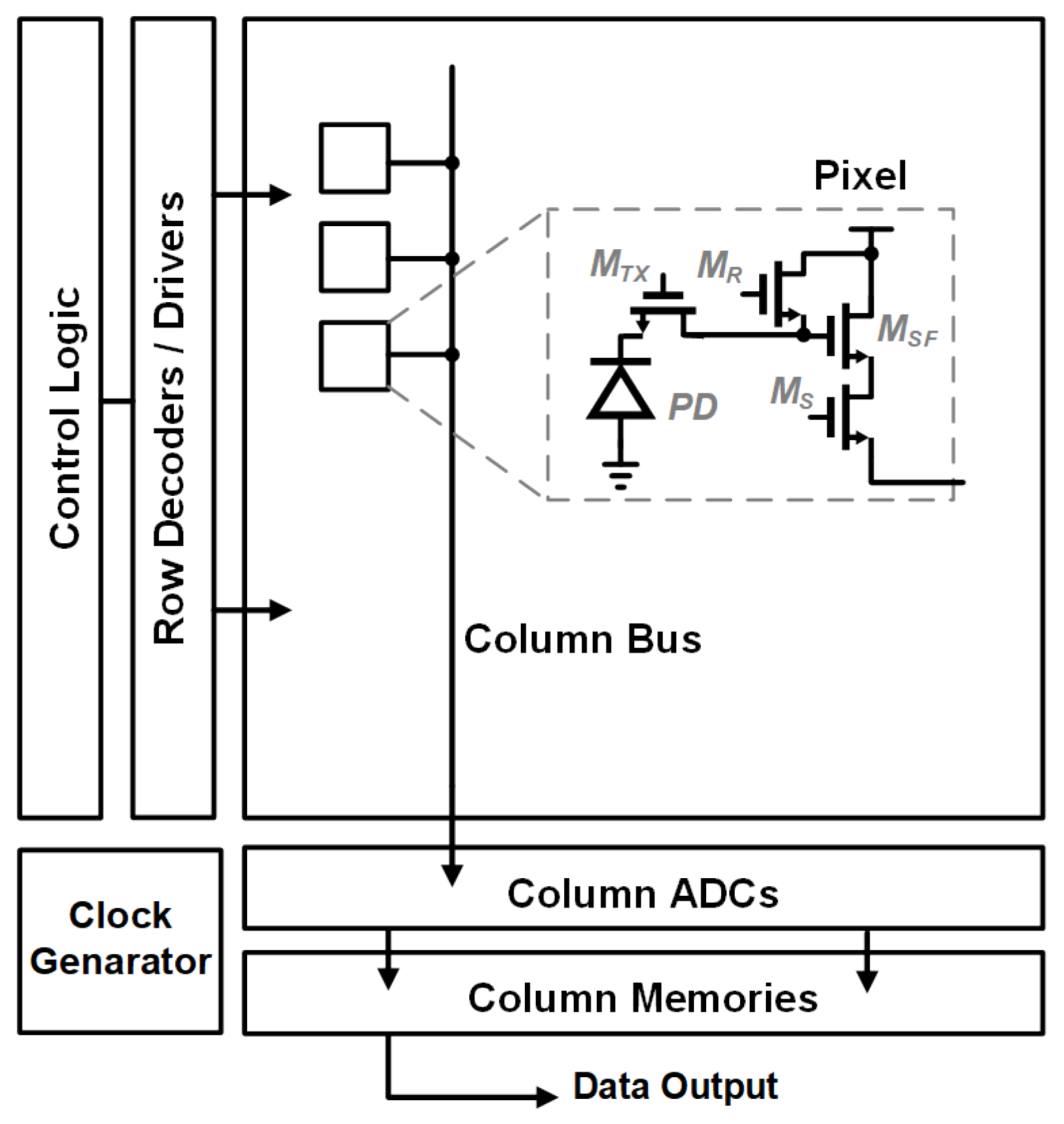
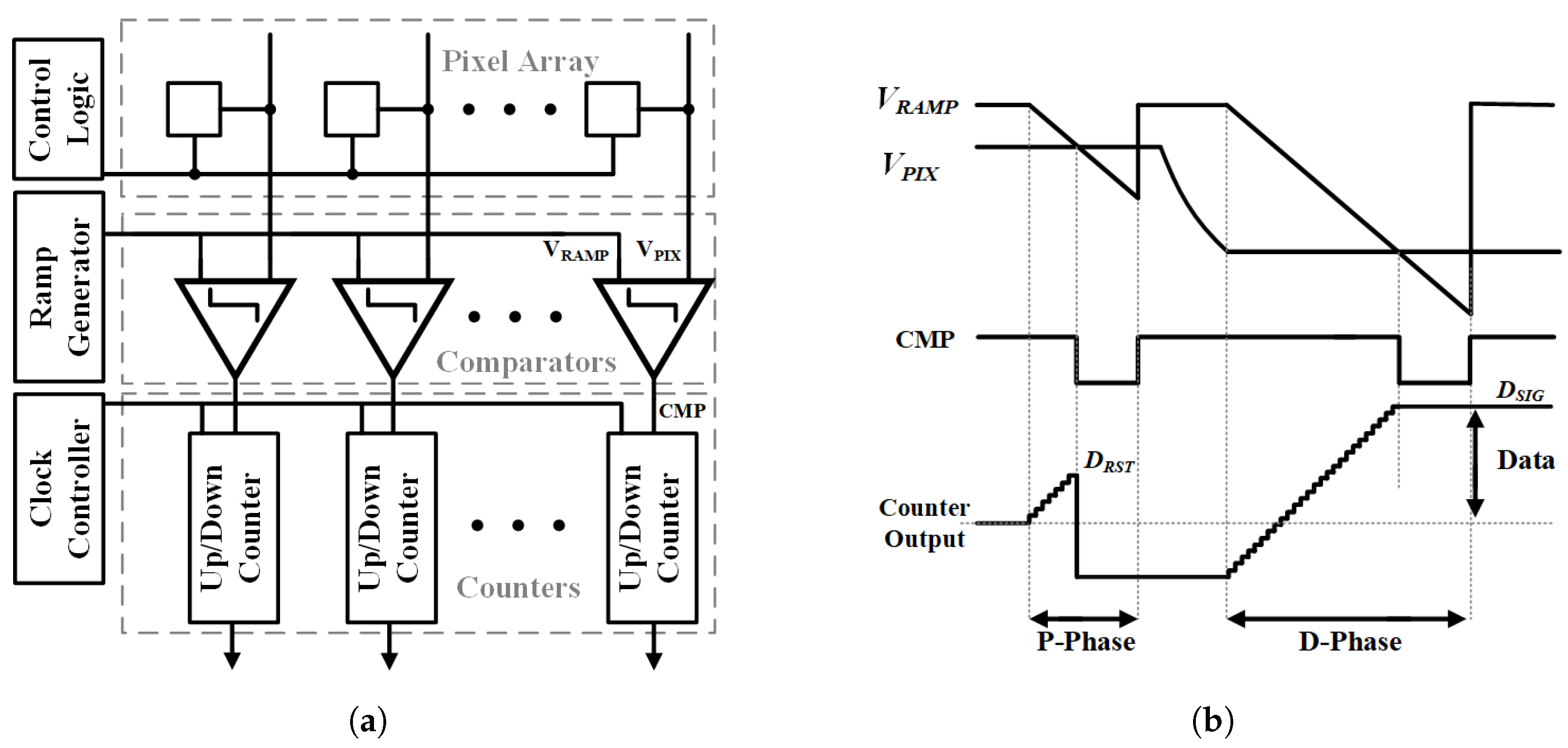
2. Overall Architecture
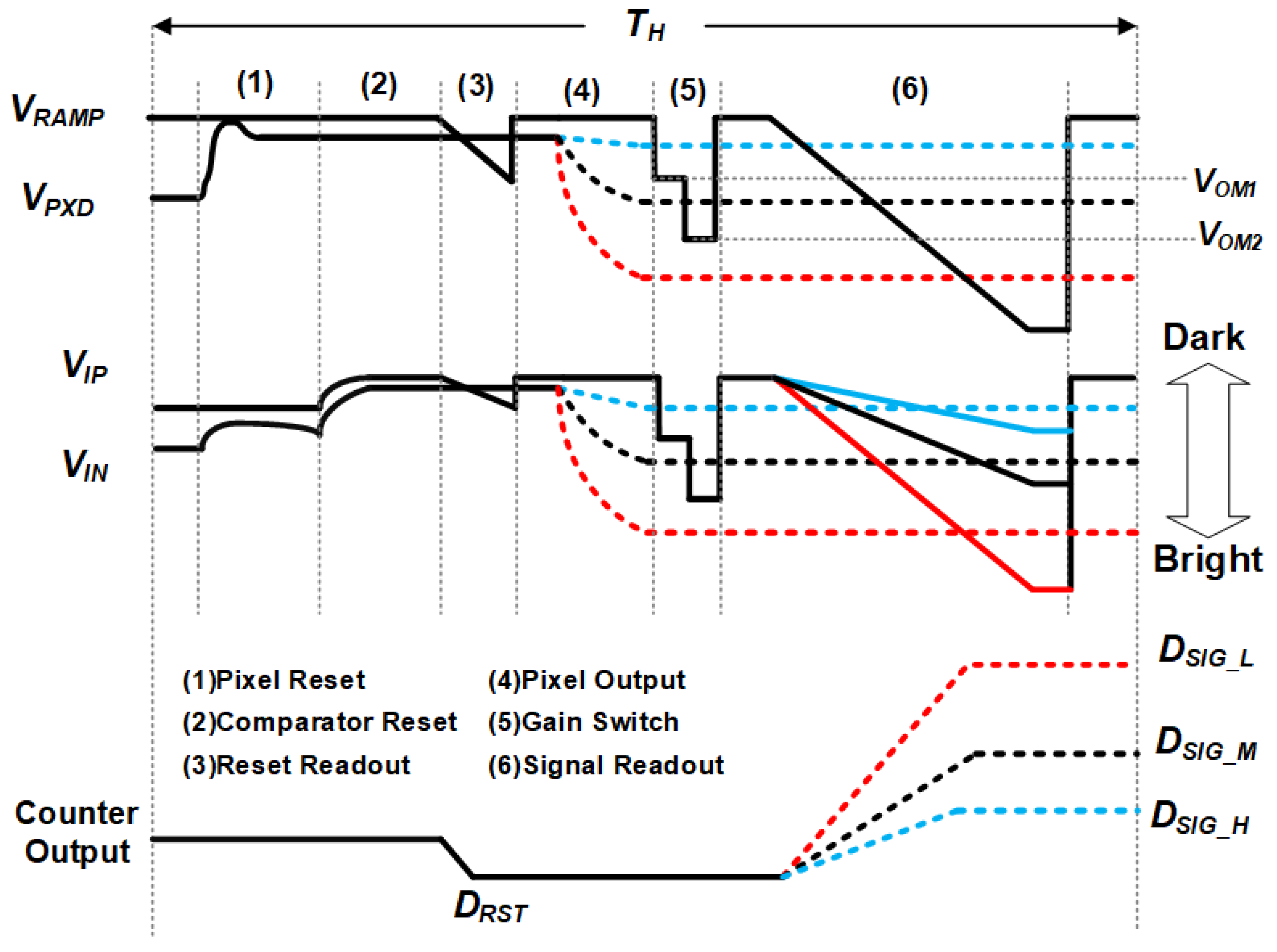
2.1. Concept of Gain-Adaptive SS-ADC
2.2. Gain Control Structure
3. Circuit Configuration
3.1. Comparator
- During the autozero period, switches S1 and S6 are closed and S5 is open. The lower plate of the capacitor is connected to the ground and the gate voltage of the transistor M6 () is equal to .
- During the comparison period, switches S1 and S6 are open and S5 is closed. The lower plate of the capacitor is connected to the boost voltage and .
- During the hold period, the switches S1 and S5 are open and S6 is closed, and is equal to .
3.2. Counter
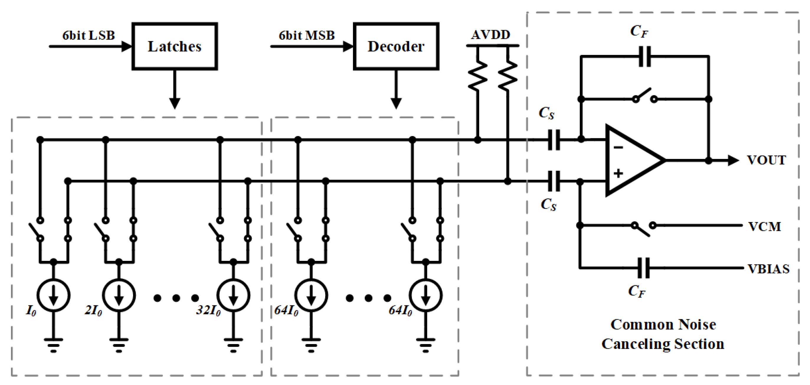
3.3. Ramp Generator
3.4. Group Delay Scheme
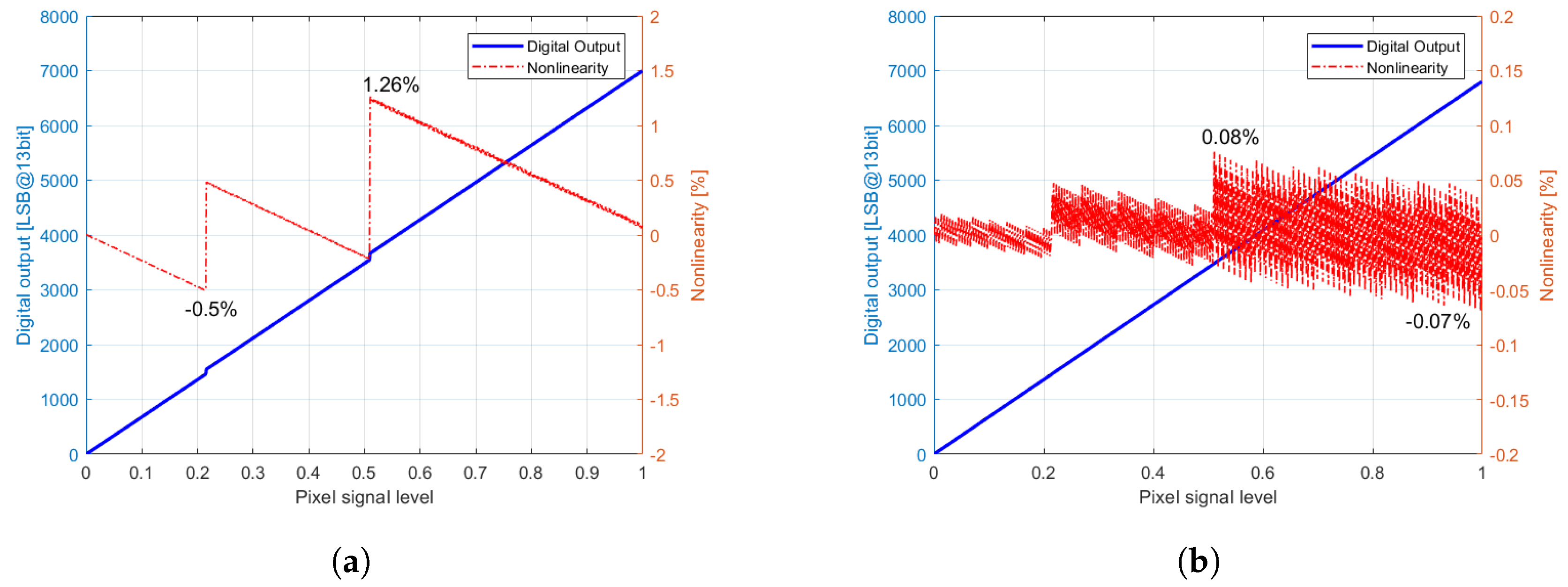
4. Nonlinearity and Calibration
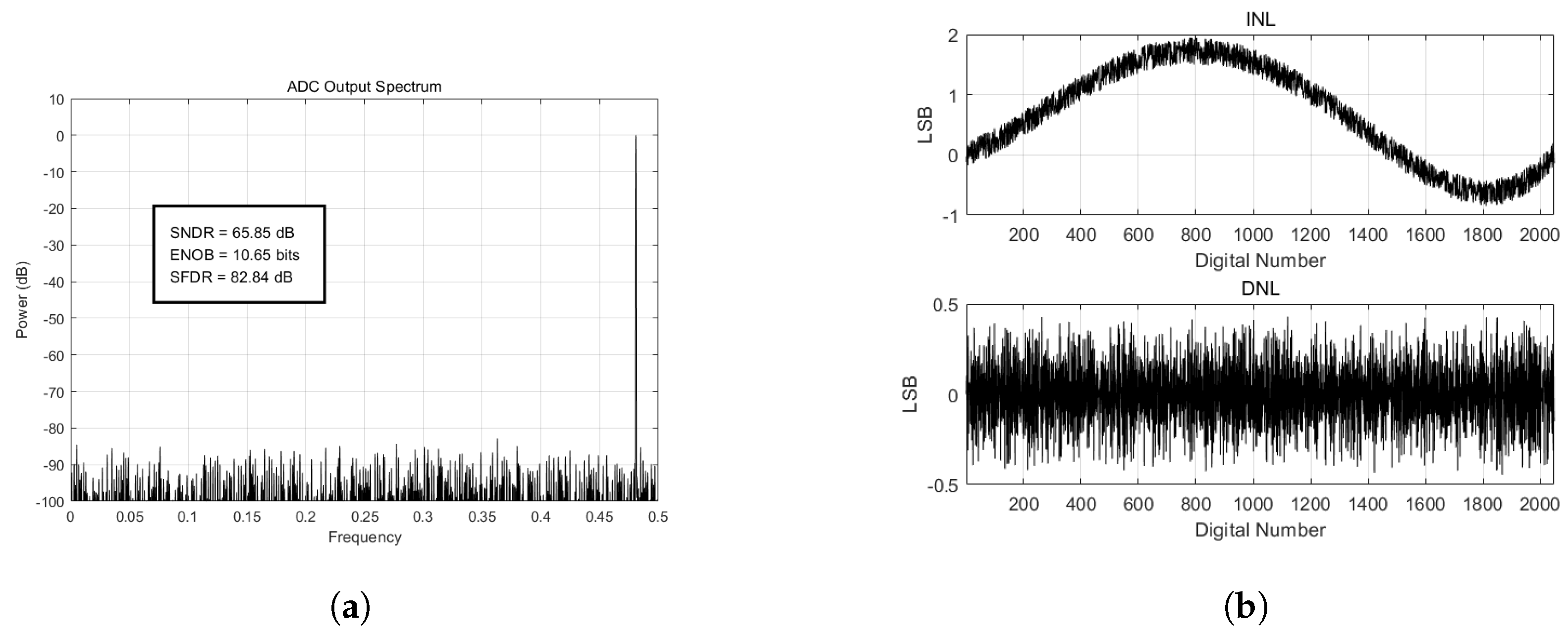
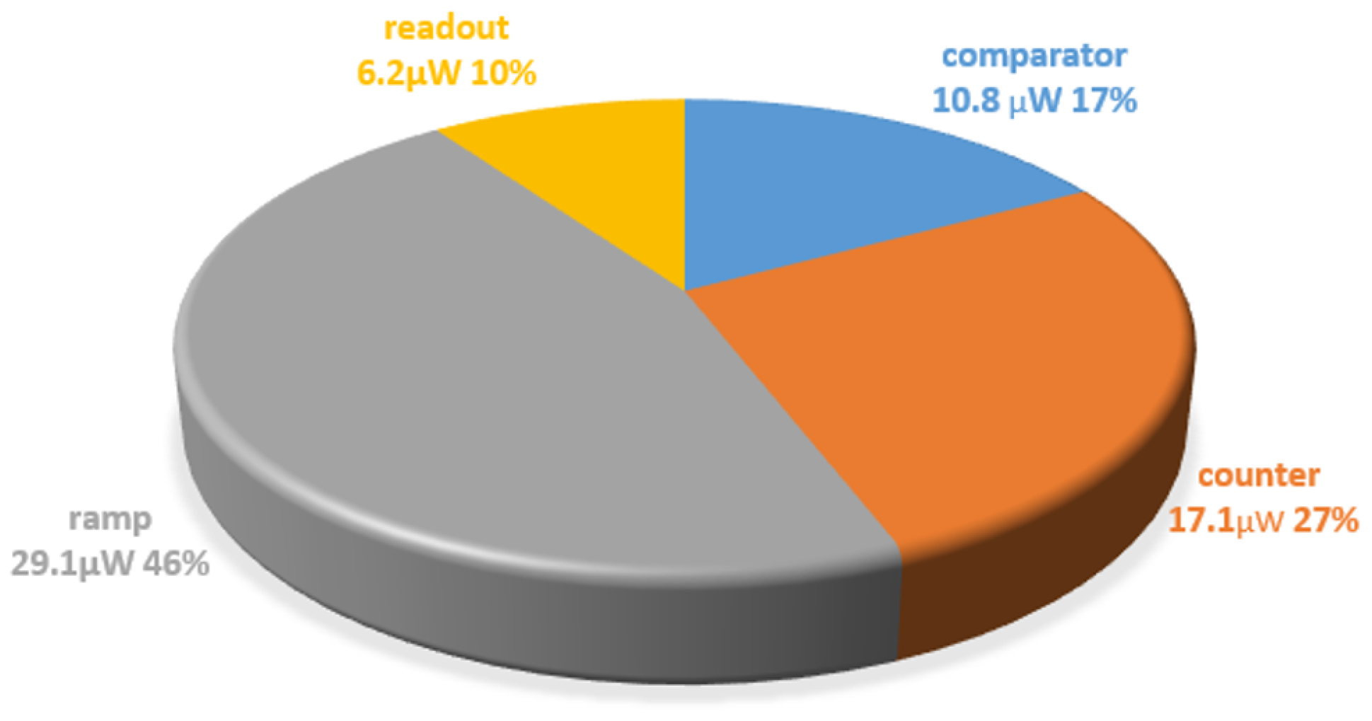
5. Experimental Results
6. Conclusions
Author Contributions
Funding
Acknowledgments
Conflicts of Interest
References
- Yoshihara, S.; Nitta, Y.; Kikuchi, M.; Koseki, K.; Ito, Y.; Inada, Y.; Kuramochi, S.; Wakabayashi, H.; Okano, M.; Kuriyama, H.; et al. A 1/1.8-inch 6.4 MPixel 60 frames/s CMOS image sensor with seamless mode change. IEEE J. Solid-State Circuits 2006, 41, 2998–3006. [Google Scholar] [CrossRef]
- Kawahito, S. Column-parallel ADCs for CMOS image sensors and their FoM-based evaluations. IEICE Trans. Electron. 2018, 101, 444–456. [Google Scholar] [CrossRef]
- Kwon, M.; Murmann, B. A New Figure of Merit Equation for Analog-to-Digital Converters in CMOS Image Sensors. In Proceedings of the 2018 IEEE International Symposium on Circuits and Systems (ISCAS), Florence, Italy, 27–30 May 2018; pp. 1–5. [Google Scholar]
- Wang, X. Noise in Sub-Micron CMOS Image Sensors. Ph.D. Thesis, Delft University, Delft, The Netherlands, 2008. [Google Scholar]
- Nakahara, T. Signal processing apparatus, control method, image pickup element, and electronic appliance with a comparison unit controlled by a control unit to provide periods of reduced electrical current. U.S Patent No. 10,491,845, 26 November 2019. [Google Scholar]
- Toyama, T.; Mishina, K.; Tsuchiya, H.; Ichikawa, T.; Iwaki, H.; Gendai, Y.; Murakami, H.; Takamiya, K.; Shiroshita, H.; Muramatsu, Y.; et al. A 17.7 Mpixel 120fps CMOS image sensor with 34.8 Gb/s readout. In Proceedings of the 2011 IEEE International Solid-State Circuits Conference, San Francisco, CA, USA, 20–24 February 2011; pp. 420–422. [Google Scholar]
- Kobayashi, M.; Onuki, Y.; Kawabata, K.; Sekine, H.; Tsuboi, T.; Muto, T.; Akiyama, T.; Matsuno, Y.; Takahashi, H.; Koizumi, T.; et al. A Temporal Noise Over 110-dB-Dynamic Range 3.4 μm Pixel Pitch Global-Shutter CMOS Image Sensor With Dual-Gain Amplifiers SS-ADC, Light Guide Structure, and Multiple-Accumulation Shutter. IEEE J. Solid-State Circuits 2018, 53, 219–228. [Google Scholar] [CrossRef]
- Baek, C.; Lim, C.; Kim, D.; Song, M. Design of a 10-bit CMOS image sensor based on an 8-bit configurable hold-and-go counter. In Proceedings of the 2012 ESSCIRC (ESSCIRC), Bordeaux, France, 17–21 September 2012; pp. 393–397. [Google Scholar] [CrossRef]
- Liu, C.C.; Mhala, M.M.; Chang, C.; Tu, H.; Chou, P.; Chao, C.; Hsueh, F. A 1.5V 33Mpixel 3D-stacked CMOS image sensor with negative substrate bias. In Proceedings of the 2016 IEEE International Solid-State Circuits Conference (ISSCC), San Francisco, CA, USA, 31 January–4 February 2016; pp. 124–125. [Google Scholar] [CrossRef]
- Liu, Q.; Edward, A.; Kinyua, M.; Soenen, E.G.; Silva-Martinez, J. A Low-Power Digitizer for Back-Illuminated 3-D-Stacked CMOS Image Sensor Readout with Passing Window and Double Auto-Zeroing Techniques. IEEE J. Solid-State Circuits 2017, 52, 1591–1604. [Google Scholar] [CrossRef]
- Park, I.; Jo, W.; Park, C.; Park, B.; Cheon, J.; Chae, Y. A 640 x 640 Fully Dynamic CMOS Image Sensor for Always-On Operation. IEEE J. Solid-State Circuits 2020. [Google Scholar] [CrossRef]
- Snoeij, M.F.; Theuwissen, A.J.; Makinwa, K.A.; Huijsing, J.H. Multiple-ramp column-parallel ADC architectures for CMOS image sensors. IEEE J. Solid-State Circuits 2007, 42, 2968–2977. [Google Scholar] [CrossRef]
- Kim, D.; Song, M. An enhanced dynamic-range CMOS image sensor using a digital logarithmic single-slope ADC. IEEE Trans. Circuits Syst. II Express Briefs 2012, 59, 653–657. [Google Scholar] [CrossRef]
- Pastorelli, C.; Mellot, P.; Mir, S.; Tubert, C. Piece-wise-linear ramp ADC for CMOS image sensor and calibration techniques. Proc. IISW 2015, 8, 204–207. [Google Scholar]
- Totsuka, H.; Tsuboi, T.; Muto, T.; Yoshida, D.; Matsuno, Y.; Ohmura, M.; Takahashi, H.; Sakurai, K.; Ichikawa, T.; Yuzurihara, H.; et al. 6.4 An APS-H-Size 250Mpixel CMOS image sensor using column single-slope ADCs with dual-gain amplifiers. In Proceedings of the 2016 IEEE International Solid-State Circuits Conference (ISSCC), San Francisco, CA, USA, 31 January–4 February 2016; pp. 116–117. [Google Scholar]
- Oike, Y.; Akiyama, K.; Hung, L.D.; Niitsuma, W.; Kato, A.; Sato, M.; Kato, Y.; Nakamura, W.; Shiroshita, H.; Sakano, Y.; et al. 8.3 M-pixel 480-fps global-shutter CMOS image sensor with gain-adaptive column ADCs and chip-on-chip stacked integration. IEEE J. Solid-State Circuits 2017, 52, 985–993. [Google Scholar] [CrossRef]
- Nitta, Y.; Muramatsu, Y.; Amano, K.; Toyama, T.; Yamamoto, J.; Mishina, K.; Suzuki, A.; Taura, T.; Kato, A.; Kikuchi, M.; et al. High-Speed Digital Double Sampling with Analog CDS on Column Parallel ADC Architecture for Low-Noise Active Pixel Sensor. In Proceedings of the 2006 IEEE International Solid State Circuits Conference—Digest of Technical Papers, San Francisco, CA, USA, 6–9 February 2006; pp. 2024–2031. [Google Scholar]
- Lim, Y.; Koh, K.M.; Kim, K.M. Double Data Rate (DDR) Counter, Analog-to-Digital Converter (ADC) Using the Same, CMOS Image Sensor Using the Same and Methods in DDR Counter, ADC and CMOS Image Sensor. U.S. Patent No. 7,990,304, 2 August 2011. [Google Scholar]
- Hisamatsu, Y. Counter, Counting Method, Ad Converter, Solid-State Imaging Device, and Electronic Device. U.S. Patent No. 9,042,508, 26 May 2015. [Google Scholar]
- Wei, J.; Xu, S.; Li, D. A Low Power Up/Down Double-Data-Rate Counter for CMOS Image Sensors. In Proceedings of the 2019 IEEE International Conference on Electron Devices and Solid-State Circuits (EDSSC), Xi’an, China, 12–14 June 2019; pp. 1–3. [Google Scholar] [CrossRef]
- Hao, C.; Liyuan, L.; Dongmei, L.; Chun, Z.; Zhihua, W. A 12-bit current steering DAC with 2-dimensional gradient-error tolerant switching scheme. J. Semicond. 2010, 31, 105006. [Google Scholar] [CrossRef]
- Deveugele, J.; Van der Plas, G.; Steyaert, M.; Gielen, G.; Sansen, W. A gradient-error and edge-effect tolerant switching scheme for a high-accuracy DAC. IEEE Trans. Circuits Syst. I Regul. Pap. 2004, 51, 191–195. [Google Scholar] [CrossRef]
- Si-Wook, Y. Ramp Signal Generator with Noise Canceling Function. U.S. Patent No. 9,331,683, 3 May 2016. [Google Scholar]
- Arai, T.; Yasue, T.; Kitamura, K.; Shimamoto, H.; Kosugi, T.; Jun, S.; Aoyama, S.; Hsu, M.; Yamashita, Y.; Sumi, H.; et al. A 1.1 μm 33Mpixel 240fps 3D-stacked CMOS image sensor with 3-stage cyclic-based analog-to-digital converters. In Proceedings of the 2016 IEEE International Solid-State Circuits Conference (ISSCC), San Francisco, CA, USA, 31 January–4 February 2016; pp. 126–128. [Google Scholar] [CrossRef]
- Kim, M.; Hong, S.; Kwon, O. An Area-Efficient and Low-Power 12-b SAR/Single-Slope ADC Without Calibration Method for CMOS Image Sensors. IEEE Trans. Electron. Devices 2016, 63, 3599–3604. [Google Scholar] [CrossRef]
- Lee, J.; Park, H.; Song, B.; Kim, K.; Eom, J.; Kim, K.; Burm, J. High Frame-Rate VGA CMOS Image Sensor Using Non-Memory Capacitor Two-Step Single-Slope ADCs. IEEE Trans. Circuits Syst. I Regul. Pap. 2015, 62, 2147–2155. [Google Scholar] [CrossRef]
- Chae, Y.; Cheon, J.; Lim, S.; Kwon, M.; Yoo, K.; Jung, W.; Lee, D.; Ham, S.; Han, G. A 2.1 M Pixels, 120 Frame/s CMOS Image Sensor with Column-Parallel ΔΣ ADC Architecture. IEEE J. Solid-State Circuits 2011, 46, 236–247. [Google Scholar] [CrossRef]


| Gain Scheme | Light Intensity | AG<1: 0> | AGB<1: 0> | Analog Gain |
|---|---|---|---|---|
| Low | High | 00 | 11 | × 1 |
| Medium | Medium | 10 | 01 | × 2 |
| High | Low | 11 | 00 | × 4 |
| [10] | [24] | [25] | [26] | [27] | This Work | |
|---|---|---|---|---|---|---|
| Process [nm] | 40 | 65 | 90 | 130 | 130 | 180 |
| Architecture | SS | Cyclic/SAR | SAR/SS | SS | SS | |
| Resolution [bit] | 12 | 12 | 12 | 12 | 12 | 13 |
| Conv. Time [s] | 2.7 | 0.92 | 2.7 | 6.4 | 2.3 | 2.6 |
| Col. Pitch [m] | 5.4 | 4.4 | 2.24 | 11.2 | 4.5 | 4.48 |
| Col. Height [m] | 610 | 920 | 998 | 590 | 600 | 310 |
| Col. Power [W] | 66.8 | 120 | 56 | 90 | 55 | 63.2 |
| DNL[LSB] | −0.28/+0.32 | −0.88/+0.82 | −0.45/+0.84 | −0.49/+1.34 | −0.55/+0.63 | −0.43/+0.46 |
| INL [LSB] | −0.94/+4.21 | −11.75/+1.04 | −1.5/+0.74 | −2.47/+2.44 | −0.8/+3.7 | −0.84/+1.95 |
| 44.0 | 27.0 | 36.9 | 140.6 | 30.9 | 20.1 | |
| 145.0 | 109.1 | 82.5 | 929.3 | 83.4 | 27.9 |
© 2020 by the authors. Licensee MDPI, Basel, Switzerland. This article is an open access article distributed under the terms and conditions of the Creative Commons Attribution (CC BY) license (http://creativecommons.org/licenses/by/4.0/).
Share and Cite
Wei, J.; Li, X.; Sun, L.; Li, D. A Low-Power Column-Parallel Gain-Adaptive Single-Slope ADC for CMOS Image Sensors. Electronics 2020, 9, 757. https://doi.org/10.3390/electronics9050757
Wei J, Li X, Sun L, Li D. A Low-Power Column-Parallel Gain-Adaptive Single-Slope ADC for CMOS Image Sensors. Electronics. 2020; 9(5):757. https://doi.org/10.3390/electronics9050757
Chicago/Turabian StyleWei, Jingwei, Xuan Li, Lei Sun, and Dongmei Li. 2020. "A Low-Power Column-Parallel Gain-Adaptive Single-Slope ADC for CMOS Image Sensors" Electronics 9, no. 5: 757. https://doi.org/10.3390/electronics9050757
APA StyleWei, J., Li, X., Sun, L., & Li, D. (2020). A Low-Power Column-Parallel Gain-Adaptive Single-Slope ADC for CMOS Image Sensors. Electronics, 9(5), 757. https://doi.org/10.3390/electronics9050757