Abstract
In this work, we present a pentacene-based organic field-effect transistor memory (OFETM) device, which employs one-step microwave-assisted hydrothermal carbon quantum dots (CQDs) embedded in a polyvinyl pyrrolidone (PVP) matrix, to form an integrated hybrid nanolayer as the charge trapping layer. The as-prepared CQDs are quasi-spherical amorphous C, with sizes ranging from 5 to 20 nm, with a number of oxygen-containing groups and likely some graphite-like domains that produce CQDs with excellent electron-withdrawing characteristics. The incorporation of CQDs into PVP dielectric materials results in a bidirectional storage property. By optimizing the concentration of CQDs embedded into the PVP matrix, the OFETM shows excellent memory characteristics with a large memory window of 8.41 V under a programming/erasing (P/E) voltage of 60 V and a retention time of up to 104 s.
1. Introduction
Organic memory devices have attracted wide attention in recent years due to their many merits over their inorganic counterparts, such as their low-cost, lightweight, solution processability, and mechanical flexibility characteristics [1,2,3]. Among the many types of organic memory devices, organic field-effect transistor memory (OFETM) devices have attracted the most attention due to their excellent properties, such as their single transistor memory cells, nondestructive readouts, compatibility with CMOS technology and potential multi-bit storage [4,5,6]. Generally, OFETM devices are divided into three types according to the charge trapping materials and the mechanism of data storage. A floating-gate OFETM device has a structure similar to that of an organic field-effect transistor (OFET) except the supplementary charge trapping units and tunneling layer which are inserted into the gate dielectric and semiconductor layer [1]. The channel current of the floating-gate OFETM device is modulated by the charges trapped in the floating gates after the programming (P)/erasing (E) pulse voltage is removed. Many materials, such as the noble metals Au, Ag, and Pt nanoparticles (NPs) [7,8,9], polymer semiconductor nanoparticles [10], carbon-based NPs [11], small molecule organic semiconductor materials [12], and transition metal dichalcogenide (TMD) monolayers [13], have been used as charge trapping units in floating-gate OFETM devices. Ferroelectric OFETM devices, in which the threshold voltage (VT) shifts on the transfer curves, have been implemented by tuning the polarization of the gate dielectric. The polarization direction in the dielectric is determined by the dipole orientation, thus directly leading to the “1” and “0” states of the memory device [14]. Common ferroelectric materials such as poly(vinylidene fluoride) (PVDF) and its copolymer poly(vinylidene fluoride-trifluoroethylene) (P(VDF-TrFE)) have been widely studied due to their large spontaneous polarizations and excellent chemical stabilities [15,16]. The third type is polymer electret OFETM devices, which use stable, solution processable, and chargeable dielectric materials inserted between the gate insulator layer and the active layer of the OFETs [17]. Different from floating-gate OFETM, polymer electret OFETM devices have a continuous charge trapping layer and can maintain the captured charges for a long time even without the tunneling layer. The possible memory mechanisms of polymer electrets are summarized as follows: (1) the orientation of permanent dipoles (in polar materials); (2) charge trapping inside the polymer electret bulk (structural defects and impurity centers); (3) charge trapping at the polymer layer/semiconductor layer interface and (or) at the polymer layer/gate insulator layer interface; and (4) charge trapping at the amorphous-crystalline interfaces (in semicrystalline polymers) and the grain boundaries (in polycrystalline materials) [18,19]. The storage capability of the polymer electret materials is determined by the chemical structures, composite ratio and morphology [17]. Baeg. et al. [18] fabricated pentacene-based OFETM devices using various chargeable thin polymer electrets layer onto silicon oxide insulating layers and investigated the effects of the hydrophobicity and polarity of polymer electrets on the properties of OFETM devices. The experimental results show that devices with hydrophobic and nonpolar polymers have nonvolatile characteristics that are superior to those of hydrophilic and polar polymers. For many p-type polymer electret OFETM devices, the influence of the negative gate pulse voltage on the transfer characteristic curves is obviously greater than that of the positive gate pulse voltage. This phenomenon is due to the high electron barrier between the semiconductor and the polymer electret materials [20]. To solve this problem, optical assistance was adopted to reduce (or displace) the positive operating pulse voltage and increase the storage windows [6]. However, there is also another method that uses select materials with strong electron withdrawing properties to be doped into polymer electrets to form integrated hybrid nanocomposites as charge trapping layers [21].
Polyvinyl pyrrolidone (PVP) is a kind of polymer electret material with moderate polarity and amphiphilic properties that is soluble in water and ethanol. Carbon quantum dot (CQD) is a new class of carbon nanomaterials that have emerged in recent years. CQDs have the advantages of low toxicity, environmental friendliness, low cost and simple synthesis methods. Due to their excellent optical properties, many studies using CQDs as light-emitting materials for organic light-emitting diodes (OLED) devices have been reported [22,23]. However, there have been few reports on CQDs used in OFETM as charge trapping sites. In this work, we will report a pentacene-based bottom gate top contact (BGTC) OFETM that uses a CQDs/PVP hybrid nanolayer as the charge trapping layer to realize bidirectional memory characteristics. The CQDs are prepared with low cost materials, and the preparation method is simple. As a result, a large memory window of 8.41 V with a relatively low programming/erasing (P/E) voltage [20] and a data retention time of up to 104 s is realized.
2. Experimental
2.1. Synthesis of the CQDs
The CQDs were prepared by a one-step microwave-assisted hydrothermal method. First, 1 g citric acid and 2 g urea were dissolved in 20 mL deionized water and stirred evenly. Then, this transparent liquid was placed into the microwave oven and heated at 750 W for 5 mins 30 s to obtain a dark, clustered solid sample. Then, the obtained reaction products were put into a vacuum drying oven at 100 °C for 1 h to remove the residual small molecule compounds. The annealed sample was dissolved in 50 mL anhydrous ethanol to obtain a CQD-ethanol saturated solution. After repeated centrifugation (8000 rpm/min, 20 mins), the upper solution was taken to obtain a green quantum-emitting CQD–ethanol solution.
2.2. Device Fabrication
Figure 1 shows the schematic of the device structure. The devices were fabricated on heavily doped Si substrates, with a 300-nm-thick SiO2 on top to form the control gate and control dielectric layer. The CQD/PVP hybrid ethanol solution was spin coated on the Si/SiO2 substrate at a speed of 2700 rpm/min to fabricate an integrated hybrid charge trapping layer, followed by annealing in a vacuum drying oven at 100 °C for 2 h to remove the residual solution. Subsequently, with the substrates at room temperature, the 50-nm-thick pentacene was deposited onto the CQDs/PVP hybrid nanolayer through vacuum deposition in a high-vacuum system at a pressure of 3 10−4 mbar, where the deposition rate was approximately 0.150.2 Å/s. Finally, 70-nm-thick Au was deposited on the pentacene through thermal evaporation on a shadow mask to fabricate the drain and source electrodes; the working pressure was 3 10−4 mbar, and the deposition rate was kept at 0.3 Å/s. The channel length and the channel width of the device were 80 and 4000 , respectively. To research the dependence of the memory characteristics on the concentration of CQDs distributed in the PVP matrix, the CQD–ethanol saturated solution and anhydrous ethanol were mixed in volume ratios of 1:1 and 1:2. Samples were prepared by taking 1 mL from each of the two different CQD–ethanol solutions and mixing them with 6 mg PVP. The corresponding samples were defined as device A (1:1) and device B (1:2). The control sample without CQDs in the PVP matrix was simultaneously prepared following the same process, which was defined as device C (6 mg PVP dissolved in 1 mL anhydrous ethanol).
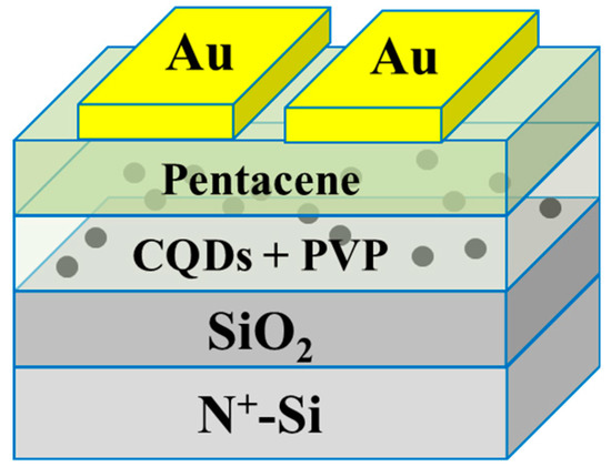
Figure 1.
Schematic of the device structure.
2.3. Characterization
The CQDs were characterized by transmission electron microscopy (TEM) and X-ray photoelectron spectroscopy (XPS). The evaporated pentacene film and Au electrode thickness were measured by a quartz monitor crystal. The surface morphology and the root mean square (RMS) surface roughness of the CQDs/PVP hybrid nanolayer and pentacene layer were characterized by atomic force microscopy (AFM). The electrical characterization of the devices was performed with a Keithley 4200-SCS semiconductor characterization system under an atmospheric environment at room temperature.
3. Results and Discussion
3.1. CQDs and Hybrid Nanolayer Characterization
In Figure 2a, the TEM image of the CQDs shows that the as-prepared CQDs are quasi-spherical nanoparticles with sizes ranging from 5 nm to 20 nm. The high-resolution TEM imagery did not exhibit a lattice structure for the CQDs. Figure 2b is the XPS C 1s spectrum of the CQDs. The C 1s peak is dominated by the C–C/C=C feature at a binding energy of approximately 284.5 eV, accompanied by the C=O feature at approximately 288.2 eV. The TEM and XPS results suggest that the CQDs are amorphous C with a number of oxygen-containing groups, and may contain some graphite-like domains that produce the as-prepared CQDs with electron-donating and/or electron-withdrawing capabilities [24].
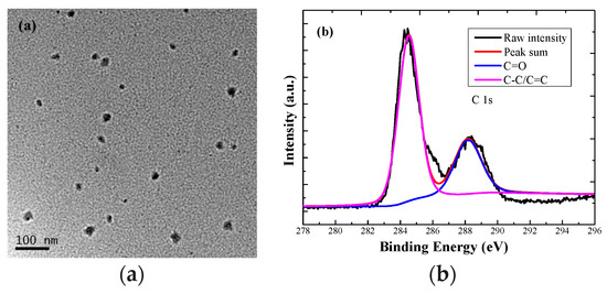
Figure 2.
(a) TEM image of the CQDs. (b) XPS C 1s spectrum of the CQDs.
In Figure 3a–c, AFM images of the charge trapping layer for devices A, B, and C are shown, and relatively smooth RMS surface roughnesses of 2.793, 4.707 and 1.918 nm are obtained, respectively. Figure 3a,b shows the microstructures of the CQDs/PVP hybrid nanolayers with different concentrations of CQDs embedded into the PVP matrix. The phase separation of the CQDs and PVP occurred during the hybrid film preparation. The aggregation of CQDs forms nano-domains which are discrete distributionin the PVP matrix. The AFM images of pentacene deposited on the corresponding nanolayers are shown in Figure 3d–f. The size distribution of the pentacene crystalline grains is 0.1–0.5 µm, which is consistent with the results reported in previous studies [25].
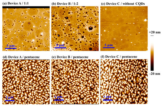
Figure 3.
Atomic force microscopy (AFM) images of different CQDs/PVP hybrid nanolayers. The CQD–ethanol saturated solution and anhydrous ethanol were mixed in volume ratios of (a) 1:1 (device A), (b) 1:2 (device B), and (c) without CQDs in PVP (device C). (d–f) AFM images of pentacene deposited on the corresponding CQDs/PVP hybrid nanolayers.
3.2. Field-Effect Characteristics of the OFETM Devices
Figure S1a–c show the output characteristics of the prepared organic field-effect transistor memory (OFETM devices), which exhibit excellent p-channel field-effect transistor characteristics in hole accumulation mode, with a drain source voltage (VDS) ranging from 0 V to −30 V, and a gate source voltage (VGS) from 10 V to −30 V in steps of −5 V (Please see supplementary materials). Figure 4a–c are the initial transfer characteristics of the three devices. The field effect mobility µ and threshold voltage (VT) of the device can be calculated using the following formula:
where Ci is the insulator capacitance per unit area, which includes the SiO2 layer and polymer layer. The channel length (L) and width (W) of these devices are 80 and 4000 µm, respectively. As shown in Figure S2, the Ci of the bilayer insulator capacitance of devices A, B, and C were 8.299, 8.201 and 8.016 nF/cm2, respectively. The calculation results fitted by the transfer characteristics curve show that the prepared OFETM devices have similar µ values of 0.0020.003 cm2/Vs. The VT of devices A, B, and C are 1.42, −1.50 and −3.99 V, respectively. The different VT values for the three devices can be explained by the distinct concentration of the CQDs in the PVP matrix. More details will be described in the following sections.
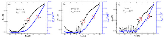
Figure 4.
(a–c) The initial transfer characteristics of devices A, B, and C.
3.3. Electrical Memory Characteristics of OFETM
Figure 5c shows the memory characteristics of device C (control sample). When the negative gate programming voltage (VP) of −60 V for 0.1 s is applied to the control sample, an obvious negative VT drift of 3.09 V is obtained. In addition, the VDS is kept at 0 V throughout the P/E operation. In our previous experiments, no obvious shifts in VT were observed under similar P operation for a pentacene-based OFET without polymer dielectric layers [26]. Thus, the negative VT shifts in device C originate from the insertion of polymer dielectric layers, either via dipolar polarization or charge trapping in the PVP layer. By comparing the storage characteristics of several electret materials with different polarizations, Baeg. et al. proved that the VT shifts in the polymer electron OFETM devices are mainly caused by the charges captured in the electret materials, not by the polarization [18]. Thus, as shown in Figure S3, the electrons transferred from the lowest unoccupied molecular orbital level (LUMO) of PVP to pentacene increase the channel electron concentration of device C, and induce a negative VT drift. Then, a positive erasing gate voltage (VE) of 60 V for 0.1 s was applied to device C. The VT has no significant shift in the positive direction. This effect is due to the electron barrier between the pentacene and PVP (0.1 eV), as shown in Figures S3 and S4. Increasing the VE time to 1 s, the transfer characteristic curves move in the positive direction, which indicates that with increasing P time, some of the hot electrons can obtain enough energy to overcome the barrier and return to the PVP layer, but the shift is still slight, as shown in Figure 5c.
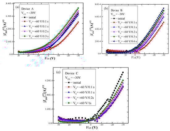
Figure 5.
(a–c) Memory characteristics of devices A, B and C.
Figure 5a,b show the memory characteristics of devices A and B, which embedded CQDs into the PVP matrix. When VP60 V for 0.1 s is applied (state 1), the negative VT drifts of devices A and B are 3.8 and 4.06 V, respectively, which slightly increases compared with device C. This drift indicates that the as-prepared CQDs have weak electron-donating properties. The electrons that cause the negative shift of VT are mainly provided by the PVP layer, but only a few by CQDs sites, as shown in Figure 6a. Then, the VE 60 V and the exerting time period from 0.1 s to 0.3 s are applied on device A (state 0). The transfer characteristic curve first returns to its initial position at 0.1 s and continues to move forward as the erasing time increases. Compared with the PVP-only device C, these bidirectional memory characteristics can be attributed to the CQDs embedded into the PVP matrix.
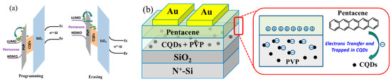
Figure 6.
(a) Energy band diagrams of devices A and B during programming/erasing (P/E) operation and (b) erasing operating mechanism for devices A and B.
The proposed erasing operating mechanism for device A that uses hybrid nanolayer as the charge storage layer is described in Figure 6. The electrons were transferred from the pentacene to the charge trapping layer and were trapped by the CQD sites under the applied positive pulse gate voltage. The as-prepared CQDs have a strong electron-withdrawing capability. One of the electron transfer mechanisms from the active layer to the CQDs is the Fowler–Nordheim (FN) tunneling mechanism, which is attributed to the low field effect mobility of the OFETM [27]. However, because the CQDs are discretely distributed in the PVP matrix, the distance between different CQDs and the pentacene/PVP interface is distinct. For CQDs close to the pentacene/PVP interface, some of the electrons in the pentacene will reach the CQDs via a direct tunneling mechanism. The electrons transferred from the pentacene to the hybrid charge trapping layer reduced the channel electron concentration and induced the positive VT drift of device A. As a result, a memory window of approximately 8.41 V was obtained for device A at VP 60 V for 0.1 s and VE 60 V for 0.3 s. Device B had the same bidirectional storage characteristics as device A. However, because the concentration of CQDs embedded into the PVP layer of device B was smaller than that of device A, under the same P/E condition (VP 60 V for 0.1 s and VE 60 V for 0.3 s), device B only obtained a 4.26 V memory window.
3.4. Retention Characteristics of Device A
Figure 7 shows the retention characteristics of device A. The retention characteristics are important indicators that reflect the capability of nonvolatile data storage in memory. In this work, the retention characteristics of device A were measured by recording IDS at both the 1 and 0 states versus time, at a reading voltage VR VGS 10 V in the dark, after a supplied VP 60 V for 0.1 s and VE 60 V for 0.3 s, respectively, as shown in Figure 7a. At state 1, the negative reading of IDS slowly increased during the whole measurement process, and this dissipation of trapped charges in the PVP layer is attributed to the internal conduction pathways that form from dipoles, moisture, and ions [18]. However, at the 0 state, IDS exhibit almost no significant change during the entire testing process, which is due to the discrete distribution and electron-withdrawing capability of the CQDs. Figure 7b shows that the memory on/off ratio of the present memory reaches 50% of the initial after 104 s, which indicates a long retention time of the device.
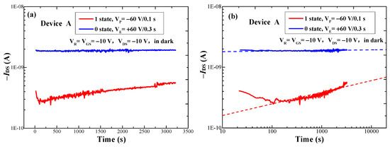
Figure 7.
Retention characteristics of device A (a) in linear and (b) exponential time coordinate.
4. Conclusions
In summary, we have demonstrated a strategy to achieve an OFETM based on a CQDs/PVP hybrid nanolayer as a charge trapping layer, and the operating mechanism is discussed in detail. In our experiment, the CQDs prepared by one-step microwave-assisted hydrothermal method have excellent electron-withdrawing properties. Embedding the CQDs into the PVP layer can improve the positive storage performance of the OFETM device. By optimizing the concentration of CQDs doped into the PVP matrix, the device A presents bidirectional memory characteristics. As a result, a large memory window of 8.41 V and a data retention time up to 104 s is realized.
Supplementary Materials
The following are available online at https://www.mdpi.com/2079-9292/9/5/753/s1, Figure S1: Output characteristics of devices A, B, and C., Figure S2: Device structure to measure the Ci of the bilayer insulator capacitance., Figure S3: Energy band diagrams of device C during programming and erasing operation., Figure S4: Energy level diagram of devices A and B without applying voltage.
Author Contributions
The contributions of all authors: conceptualization, W.Z. and J.Y. (Jianhong Yang); methodology, W.Z. and J.Y. (Jianhong Yang); investigation, W.Z., X.G. and J.Y. (Jinchao Yin); writing—original draft preparation, W.Z. and J.Y. (Jianhong Yang); writing—review and editing, W.Z., J.Y. (Jianhong Yang) and X.G. All authors have read and agreed to the published version of the manuscript.
Funding
This research received no external funding.
Conflicts of Interest
The authors declare no conflict of interest.
References
- Zhou, L.; Mao, J.; Ren, Y.; Han, S.T.; Roy, V.A.L.; Zhou, Y. Recent Advances of Flexible Data Storage Devices Based on Organic Nanoscaled Materials. Small 2018, 14, 1703126. [Google Scholar] [CrossRef] [PubMed]
- Au-Duong, A.N.; Kuo, C.C.; Chiu, Y.C. Self-assembled oligosaccharide-based block copolymers as chargestorage materials for memory devices. Polym. J. 2018, 50. [Google Scholar]
- Wu, C.; Wang, W.; Song, J. Solution Processed Top-gate High-Performance Organic Transistor Nonvolatile Memory with Separated Molecular Microdomains Floating-Gate. IEEE Electron Dev. Lett. 2017, 38, 641. [Google Scholar] [CrossRef]
- Wang, W.; Han, J.; Ying, J.; Xie, W. MoO3 Modification Layer to Enhance Performance of Pentacene-OTFTs With Various Low-Cost Metals as Source/Drain Electrodes. IEEE. T. Electron. Dev. 2014, 61, 3507. [Google Scholar] [CrossRef]
- Han, J.; Wang, W.; Ying, J.; Xie, W. Ambipolar organic thin-film transistor-based nano-floating-gate nonvolatile memory. Appl. Phys. Lett. 2014, 104, 013302. [Google Scholar] [CrossRef]
- Guo, Y.; Di, C.; Ye, S.; Sun, X.; Zheng, J.; Wen, Y.; Wu, W.; Yu, G.; Liu, Y. Multibit Storage of Organic Thin-Film Field-Effect Transistors. Adv. Mater. 2009, 21, 1954. [Google Scholar] [CrossRef]
- Wang, K.; Ling, H.; Bao, Y.; Yang, M.; Yang, Y.; Hussain, M.; Wang, H.; Zhang, L.; Xie, L.; Yi, M.; et al. A Centimeter-Scale Inorganic Nanoparticle Superlattice Monolayer with Non-Close-Packing and its High Performance in Memory Devices. Adv. Mater. 2018, 30, 1800595. [Google Scholar] [CrossRef]
- Gupta, R.K.; Kusuma, D.Y.; Lee, P.S.; Srinivasan, M.P. Copper nanoparticles embedded in a polyimide film for non-volatile memory applications. Mater. Lett. 2012, 68, 287. [Google Scholar] [CrossRef]
- Haik, M.Y.; Ayesh, A.I.; Abdulrehman, T.; Haik, Y. Novel organic memory devices using Au–Pt–Ag nanoparticles as charge storage elements. Mater. Lett. 2014, 124, 67. [Google Scholar] [CrossRef]
- Shih, C.C.; Chiu, Y.C.; Lee, W.Y.; Chen, J.Y.; Chen, W.C. Conjugated Polymer Nanoparticles as Nano Floating Gate Electrets for High Performance Nonvolatile Organic Transistor Memory Devices. Adv. Funct. Mater. 2015, 25, 1511. [Google Scholar] [CrossRef]
- Ji, Y.; Kim, J.; Cha, A.N.; Lee, S.A.; Lee, M.W.; Suh, J.S.; Bae, S.; Moon, B.J.; Lee, S.H.; Lee, D.S.; et al. Graphene quantum dots as a highly efficient solution-processed charge trapping medium for organic nano-floating gate memory. Nanotechnology 2016, 27, 145204. [Google Scholar] [CrossRef] [PubMed]
- Chang, H.C.; Lu, C.; Liu, C.L.; Chen, W.C. Single-Crystal C60 Needle/CuPc Nanoparticle Double Floating-Gate for Low-Voltage Organic Transistors Based Non-Volatile Memory Devices. Adv. Mater. 2015, 27, 27. [Google Scholar] [CrossRef] [PubMed]
- Kang, M.; Kim, Y.A.; Yun, J.M.; Khim, D.; Kim, J.; Noh, Y.Y.; Baeg, K.J.; Kim, D.Y. Stable charge storing in two-dimensional MoS2 nanoflake floating gates for multilevel organic flash memory. Nanoscale 2014, 6, 12315. [Google Scholar] [CrossRef] [PubMed]
- Liang, L.; He, W.; Cao, R.; Wei, X.; Uemura, S.; Kamata, T.; Nakamura, K.; Ding, C.; Liu, X.; Kobayashi, N. Non-Volatile Transistor Memory with a Polypeptide Dielectric. Molecules 2020, 25, 499. [Google Scholar] [CrossRef]
- Bae, I.; Kang, S.J.; Park, Y.J.; Furukawa, T.; Park, C. Organicferroelectric field-effect transistor with P(VDF-TrFE)/PMMA blend thin films for non-volatile memory applications. Curr. Appl. Phys. 2010, 10, e54. [Google Scholar] [CrossRef]
- Xu, M.; Guo, S.; Xiang, L.; Xu, T.; Xie, W.; Wang, W. High Mobility Flexible Ferroelectric Organic Transistor Nonvolatile Memory With an Ultrathin AlOX Interfacial Layer. IEEE T. Electron. Dev. 2018, 65, 1113. [Google Scholar] [CrossRef]
- Chou, Y.H.; Chang, H.C.; Liu, C.L.; Chen, W.C. Polymeric charge storage electrets for non-volatile organic field effect transistor memory devices. Polym. Chem. 2015, 6, 341. [Google Scholar] [CrossRef]
- Baeg, K.J.; Noh, Y.Y.; Ghim, J.; Lim, B.; Kim, D.Y. Polarity Effects of Polymer Gate Electrets on Non-Volatile Organic Field-Effect Transistor Memory. Adv. Funct. Mater. 2008, 18, 3678. [Google Scholar] [CrossRef]
- Dao, T.T.; Matsushima, T.; Murata, H. Organic nonvolatile memory transistors based on fullerene and an electron-trapping polymer. Org. Electron. 2012, 13, 2709. [Google Scholar] [CrossRef]
- Baeg, K.J.; Noh, Y.Y.; Ghim, J.; Kang, S.J.; Lee, H.; Kim, D.Y. Organic Non-Volatile Memory Based on Pentacene Field-Effect Transistors Using a Polymeric Gate Electret. Adv. Mater. 2006, 18, 3179. [Google Scholar] [CrossRef]
- Baeg, K.J.; Khim, D.; Kim, D.Y.; Jung, S.W.; Koo, J.B.; Noh, Y.Y. Organic Nano-Floating-Gate Memory with Polymer: [6,6]-Phenyl-C61 Butyric Acid Methyl Ester Composite Films. J. Appl. Phys. 2010, 49, 05EB01. [Google Scholar] [CrossRef]
- Lim, S.Y.; Shen, W.; Gao, Z. Carbon quantum dots and their applications. Chem. Soc. Rev. 2014, 44, 362. [Google Scholar] [CrossRef] [PubMed]
- Qian, K.; Li, H.; Zheng, B.; Chang, F.; Lei, Q.; Han, G.; Song, Y.; Liu, S.; Wei, Y. Modulation effect of carbon quantum dots in organic electroluminescent devices. Org. Electron. 2017, 51, 314. [Google Scholar] [CrossRef]
- Liu, J.; Liu, C.H.; She, X.J.; Sun, Q.J.; Gao, X.; Wang, S.D. Organic field-effect transistor nonvolatile memories utilizing sputtered C nanoparticles as nano-floating-gate. Appl. Phys. Lett. 2014, 105, 163302. [Google Scholar] [CrossRef]
- Sarkar, K.J.; Pal, B.; Banerji, P. Graphene Oxide as a Dielectric and Charge Trap Element in Pentacene-Based Organic Thin-Film Transistors for Nonvolatile Memory. ACS Omega 2019, 4, 4312. [Google Scholar] [CrossRef] [PubMed]
- Zhang, W.T.; Wang, F.X.; Li, Y.M.; Guo, X.X.; Yang, J.H. Organic field-effect transistor floating-gate memory devices using polysilicon as charge trapping layer. Chin. Phys. B 2019, 28, 086801. [Google Scholar] [CrossRef]
- Liu, Z.; Xue, F.; Su, Y.; Lvov, Y.M.; Varahramyan, K. Memory Effect of a Polymer Thin-Film Transistor with self-assembled gold nanoparticles in the gate dielectric. IEEE T Nanotechnol 2006, 5, 379. [Google Scholar]
© 2020 by the authors. Licensee MDPI, Basel, Switzerland. This article is an open access article distributed under the terms and conditions of the Creative Commons Attribution (CC BY) license (http://creativecommons.org/licenses/by/4.0/).