Abstract
Recently, many non-conventional three-phase inverters, topologies for green energy source grid-connection systems, and electric drives have been proposed. Simplifying the inverter circuit is crucial to analyze and solve their models in order to design them. The main goal of the study is centered on obtaining a single-phase equivalent circuit and space state model from non-conventional three-phase inverters based on bidirectional direct current–direct current (DC–DC) Buck-Boost topology using isolated gate bipolar transistors (IGBT). From just one phase of the three-phase inverter, the single-phase equivalent circuit was obtained by means of Kirchhoff’s laws. The equivalent circuit operation steps were presented in order to obtain the space state model. Finally, the equivalent circuit was simulated, and experimental results with a 200 W three-phase inverter feeding a resistive, inductive, and capacitive loads were performed to confirm the theoretical and simulation analyses. The results show the state space dynamic behavior variables of single-phase and three-phase models are quite similar. Therefore, it can be concluded that the proposed circuit can be used with property to represent equivalent single-phase models of non-conventional three-phase inverters.
1. Introduction
Alternating current (AC) voltages generated with amplitudes greater than the input source voltage are among the basic prerequisites in many applications such as three-phase electric drives, green energy sources, and uninterruptible power supply (UPS) systems, among others. The single-stage non-conventional inverters’ topologies research for these applications have been increased lately [1,2,3,4]. In most of the cases, analyzing and solving the models are not simple due to the high system order and complex equations. Then, simplifying the inverter circuit in order to reduce its order model leads to a computational effort reduction. Consequently, it become more suitable in real-time control system applications [5].
Among the non-conventional inverters, the direct current–alternating current (DC–AC) topology based in DC–DC Buck-Boost converters has been noticed due to the possibility to obtain output voltage higher or lower than the input voltage. The Boost topology is not suitable for this application due to the fact that it yields an output voltage higher than or equal to the input voltage. In [6], the analysis of a single-phase inverter was presented based on two DC–DC bi-directional Buck-Boost converters, but all analysis was made using the full model of inverter. In [7], a single-phase differential DC–AC Buck-Boost converter is analyzed, and a novel control technique for variable frequency applications is proposed.
Usually, the DC–AC Buck-Boost application is focused in PV systems using single-phase inverters, such as [8,9,10,11,12], without using three-phase topologies due to its complexity. A three-phase Buck-Boost AC voltage regulator with twelve switches was presented in 2016 [13], and, in [14], simulation results of a six switch three-phase Buck-Boost inverter with resistive load. However, none of them approached a simplified model of the inverter for analysis and simulation purposes.
Recently, many topologies using Buck-Boost converters as a DC–AC converter has been increased such as presented in [15], where it was proposed an inverter with three Buck-Boost converters in bridge topology. In [16], a bidirectional twisted single-phase single-stage Buck-Boost DC–AC converter is described for applications with PV arrays or storage batteries, and, in [17], a single-stage isolated three-phase four-leg inverter has been proposed.
In this paper, the single-phase space state model and equivalent circuit of the non-conventional three-phase inverter with six IGBTs, based on Buck-Boost topology, is proposed. The full six order model for a resistive load is presented, and the simplification circuit obtained by reducing the full model to a simplified second order model, taking one leg of the inverter as reference. The simulations performed in the PLECS software to compare results of single-phase and three-phase circuit inverters for a resistive load confirm the advantages of using the simplified model. Finally, a three-phase 200 W buck–boost DC–AC converter prototype with resistive, inductive, and capacitive loads are implemented in order to obtain experimental results to support simulations and confirm that the theoretical proposed analyses are in accordance. The results show that the proposed circuit and model achieve a reliable and accurate solution that can be used to design and represent the dynamic behavior of a full model inverter in steady state.
2. The Three-Phase Line Voltages
The three-phase Buck-Boost inverter analyzed in this paper is shown in Figure 1. The converter is based in three bi-directional DC–DC Buck-Boost converters (legs 1, 2, and 3), which are able to generate three-phase AC voltages whose peak values can be greater or lower than the DC input voltage in a single stage. If each Buck-Boost converter is controlled to track DC-biased (unipolar) sinusoidal references that are phase shifted by 120 from one another, the output line voltages will be a three-phase balanced sinusoidal system.
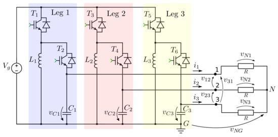
Figure 1.
Three-phase Buck-Boost inverter topology.
The capacitors’ voltage references can be written as shown in Equation (1):
The terms and represent the DC-bias and the sinusoidal voltage component of capacitors, respectively, where represents the phase or inverter leg.
The line voltages are given by:
Consequently:
Based on Equations (2)–(4), these results give rise to the conclusion that , and are pure sinusoidal voltages with no DC-bias.
The Load Phase Voltages
Taking the float N reference, and considering that the three-phase load is balanced, it can be shown that:
Expanding the Equations (6) for all three-phases and adding them yields:
3. Mathematical Model
3.1. The Three-Phase Model
The non-conventional three-phase inverter space state model shown in Figure 1 is given by Equation (9). In order to obtain the full model, each leg equation was derived through the determination of the respective line current in function of the load and capacitors’ voltages. The modeling does not take into account the non-idealities of the inverter components. This space state representation was obtained taking into consideration the continuous conduction model of operation and the balanced three-phase load, even though this model can be used under unbalanced loads. This application will not be analyzed in this work since a single-phase model can only be useful for balanced systems.
3.2. The Equivalent Single-Phase Circuit Model
In order to obtain the equivalent single-phase circuit model, one of the inverter legs was taken as reference. For convenience, the first leg was chosen as shown in Figure 2, where Z represents the equivalent load of leg 1 equivalent circuit.
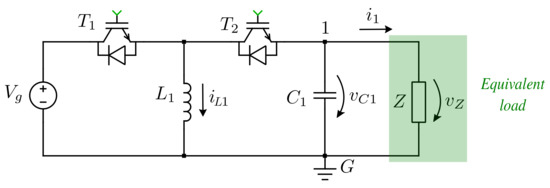
Figure 2.
Leg 1 equivalent circuit.
Taking the Equation (5), the load voltage can be obtained in accordance with the following steps:
From Equation (10), it can be concluded that the equivalent load Z can be replaced by a load resistance in series with a DC source. By doing so, the equivalent single-phase circuit model of single stage Buck-Boost three-phase inverters can be represented by the electric circuit shown in Figure 3.
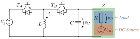
Figure 3.
Single-phase equivalent circuit.
The DC source voltage level does not affect the AC output voltage, since its value is greater than the peak sinusoidal value of capacitor voltages, in order to avoid negative voltage at capacitors. In this work, the DC voltage level of capacitors is determined from Equation (11):
The adopted value for in the simulation and prototype was .
3.2.1. Steps of Operation
Due to the bi-directional current characteristics in each switch of equivalent circuit model presented in Figure 3, the converter will operate differently in each half cycle R load voltage, as shown in Figure 4. In the positive half cycle, only the IGBT can conduct when switched and diode can be forward biased. On the other hand, in the negative half cycle, only the IGBT can conduct when switched and the diode can be forward biased, as can be seen in Figure 5a and Figure 6a.
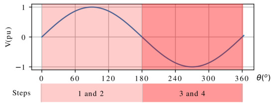
Figure 4.
Steps of operation in each half cycle of R load voltage.
Then, the following operation steps in continuous conduction mode can be for each half cycle:
- Positive half cycle:
 Figure 5. Operation steps of equivalent single-phase model in the positive half cycle: (a) Step 1; (b) Step 2.Step 1: In this step, only the IBGT of switch is ON, and the switch B is OFF. During this step, the inductor is charged and the capacitor supplies energy to the resistive load and the source, as shown in Figure 5a.Step 2: In this case, only the diode of switch is ON, and the switch A is OFF. During this step, the inductor charges the capacitor and supply energy to the resistive load and the source, as shown in Figure 5b.
 - Negative half cycle:
 Figure 6. Operation steps of equivalent single-phase model in the negative half cycle: (a) Step 3; (b) Step 4.Step 3: In this step, only the diode of switch is ON, and the switch B is OFF. Now, the inductor supplies energy to the source. The source supplies energy to the resistive load and charges the capacitor, as shown in Figure 6a.Step 4: In this case, only the IGBT of switch is ON, and the switch A is OFF. Here, the inductor is charged from the source and the capacitor. The resistive load is supplied by source also. Figure 6b shows this step.
3.2.2. The Single-Phase Space State Model
As the power converter includes the duty cycle operation, the linear system analysis needs to be derived according to its operation steps described in the last section for each operation region.
Positive half cycle:
Considering and as state variables, Equations (12), (13) and (14) can be collected into state space representation given by
Negative half cycle:
Comparing the obtained equations from operation steps 1 and 2, it can be concluded that these steps have identical linear equations. The same is observed when comparing steps 3 and 4. This simplification is only possible because the semiconductors and inverter passive elements non-idealities were not taken into account.
Since then, the average state equations for the negative and positive half cycles will be the same. This conclusion rise up the average state equations that describe the equivalent single-phase space state model can be given by (30) and (31).
From Equation (30), the ideal duty cycle ratio function can be obtained, given by:
Applying Equation (32) to a single-phase equivalent model, the duty cycle ratio can be expressed as:
The same equation can be applied to each leg of three-phase Buck-Boost inverter. As a result:
Stationary inductor and capacitor waveforms can be drawn from Equations (12)–(14), (17)–(19), (24)–(26) and (27)–(29), as shown in Figure 7a,b, respectively:
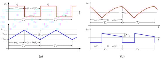
Figure 7.
Stationary waveforms of inductors and capacitors: (a) Inductor waveforms; (b) Capacitor waveforms.
4. Simulation Results
In order to validate the presented theory, simulations were performed in the PLECS software for three-phase and equivalent single-phase circuits shown in Figure 1 and Figure 3, respectively, working in open-loop. The results presented here were obtained for the following specifications shown in Table 1. The schematic circuit simulating a three-phase inverter and its equivalent single-phase circuit on PLECS are shown in Figure 8 and Figure 9, respectively. The simulation results were obtained for three load types: R load, RL load, and RC load. The RL case simulated a load transient condition in order to analyze the behavior of single-phase model under variable loads, in comparison with the full model.

Table 1.
Main parameters of the inverter.
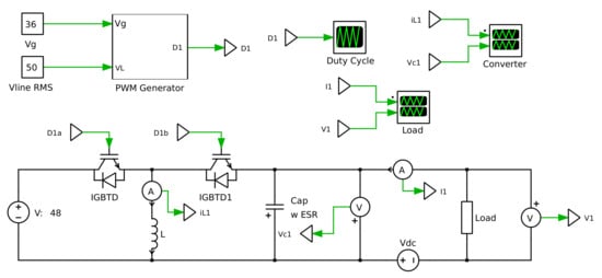
Figure 8.
Single-phase equivalent circuit model PLECS schematic.
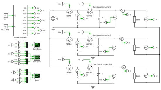
Figure 9.
Three-phase inverter PLECS schematic.
The duty-cycle was calculated in accord with Equations (33) and (34) for single-phase and three-phase models, respectively. Their waveforms are presented in Figure 10.
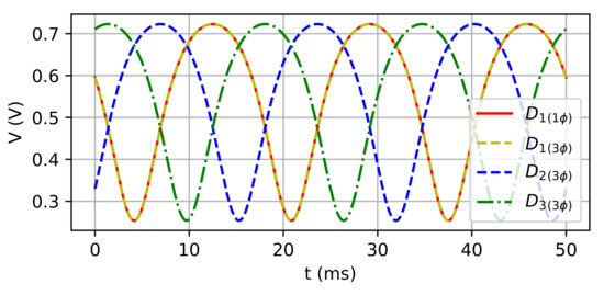
Figure 10.
Duty cycle.
4.1. R Load
In this case, a pure resistive load is simulated. The main three-phase inverter circuit waveforms in steady state are presented in Figure 11, Figure 12 and Figure 13. In Table 2, the RMS (root mean square), average, and peak-to-peak values for the currents and voltages are presented.
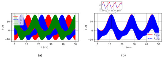
Figure 11.
Inductor currents for R load case: (a) Three-phase model; (b) Single-phase and three-phase
(leg 1) models.
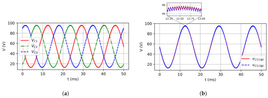
Figure 12.
Capacitor voltages for R load case: (a) Three-phase model; (b) Single-phase and three-phase
(leg 1) models.
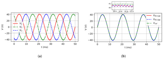
Figure 13.
Load phase voltages for R load case: (a) Three-phase model; (b) Single-phase and three-phase
(leg 1) models.
Table 2.
RMS (root mean square), average and peak-to-peak values for the simulated currents and voltages: R load.
Figure 11a,b show, respectively, the three-phase model inductor currents and the comparison between the inductor currents of three-phase and single-phase models. Figure 12a,b show the three-phase model voltage capacitors, and the comparison of three-phase and single-phase models, respectively. Finally, Figure 13a,b show the three-phase model load phase voltage and the comparison for single and three-phase models, respectively. The small difference between both models and the reference is due to the inverter running in open-loop mode and there is no control of the output voltage inverter. On the other hand, these differences do not invalidate the proposed model. The calculus approximation can also yield some differences between the final values compared with the expected values.
As it can be observed, the inductor currents and capacitor voltages for both models are quite similar as expected. The instantaneous average output load voltage for both models are very close to the expected reference waveform as shown in Figure 13b. This proves that the simulations performed have shown the single-phase model can represent with exactness the dynamic behavior of three-phase inverters in steady state.
4.2. RL Load
In this scenario, a Ω resistor in series with a 22.1 mH inductor is simulated, whose impedance in 60 Hz is about , with a power factor about 0.82. The main three-phase inverter circuit waveforms in steady state are presented in Figure 14, Figure 15, Figure 16 and Figure 17. In Table 3, the RMS (root mean square), average, and peak-to-peak values for the currents and voltages are presented.
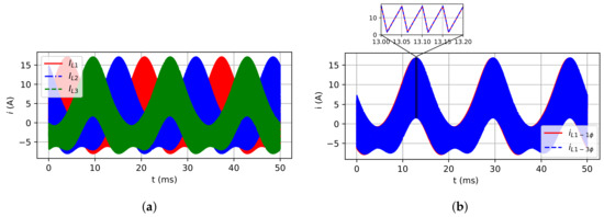
Figure 14.
Inductor currents for RL load case: (a) Three-phase model; (b) Single-phase and three-phase
(leg 1) models.
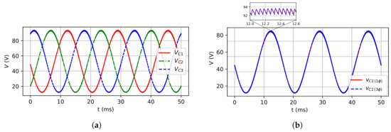
Figure 15.
Capacitor voltages for RL load case: (a) Three-phase model; (b) Single-phase and three-phase
(leg 1) models.
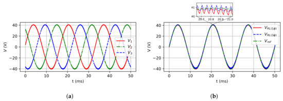
Figure 16.
Load phase voltages for RL load case: (a) Three-phase model; (b) Single-phase and
three-phase (leg 1) models.
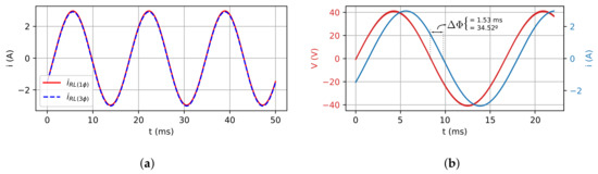
Figure 17.
RL load case: (a) Load phase currents of single-phase and three-phase (leg 1) models; (b)
Load phase voltage and current of the single-phase model.
Table 3.
RMS (root mean square), average, and peak-to-peak values for the simulated currents and voltages: RL load.
Figure 14a,b show, respectively, the three-phase model inductor currents and the comparison between the inductor currents of three-phase and single-phase models. Figure 15a,b show the three-phase model capacitor voltages and the comparison of three-phase and single-phase models, respectively. Figure 16a,b show the three-phase model load phase voltage and the comparison for single and three-phase models, respectively. As it can be observed, the inductors’ currents and capacitors’ voltages are quite similar as expected, as well as for the load phase voltage. Finally, Figure 17a shows the comparison between load current for both models, and Figure 17b shows the voltage and current at the RL load, where the shifting between them equal to 34.52 can be observed, confirming that the power factor expected ().
4.3. RC Load
In this scenario, a 6 resistor in series with 235 F capacitor is simulated, whose impedance in 60 Hz is about 6 + j11.29 with a power factor about 0.43. The main three-phase inverter circuit waveforms in steady state are presented in Figure 18, Figure 19, Figure 20 and Figure 21. In the Table 4, the RMS (root mean square), average, and peak-to-peak values for the currents and voltages are presented.
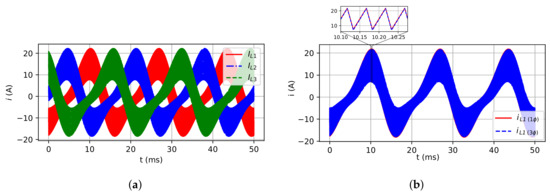
Figure 18.
Inductor currents for RC load case: (a) Three-phase model; (b) Single-phase and three-phase
(leg 1) models.
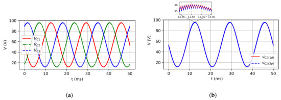
Figure 19.
Capacitor voltages for RC load case: (a) Three-phase model; (b) Single-phase and three-phase
(leg 1) models.
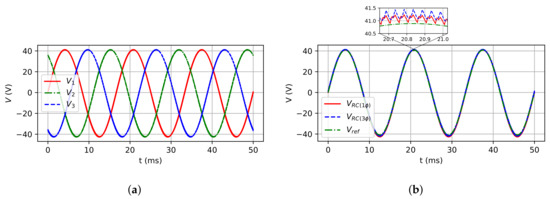
Figure 20.
Load phase for RC load case: (a) Three-phase model; (b) Single-phase and three-phase
(leg 1) models.
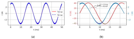
Figure 21.
RC load case: (a) Load phase currents of single-phase and three-phase (leg 1) models;
(b) Load phase voltage and current of the single-phase model.
Table 4.
RMS (root mean square), average, and peak-to-peak values for the simulated currents and voltages: RC load.
Figure 18a,b show, respectively, the three-phase model inductor currents and the comparison between the inductor currents of three-phase and single-phase models. Figure 19a,b show the three-phase model voltage capacitors, and the comparison of three-phase and single-phase models, respectively. Figure 20a,b show the three-phase model load phase voltage, and the comparison for single and three-phase models, respectively. As it can be observed, the inductors’ currents and capacitors’ voltages are quite similar as expected, as well as for the load phase voltage. Finally, Figure 21a shows the comparison between load current for both models, and Figure 21b shows the voltage and current at RC load. The shifting between them of 62.62 can be observed that confirms the power factor expected ().
4.4. RL Load with Transient
The series RL load in this case is initially made by a 24.7 equivalent resistance with a 22.1 mH inductor, whose impedance in 60 Hz is about 24.7 + j8.26 . After 100 ms, the resistive part is decreased by 10 during 200 ms. Then, the resistive part goes back to its original value. Figure 22 shows the waveforms of RL load current and voltage waveforms, and state variables for single-phase and three-phase models.
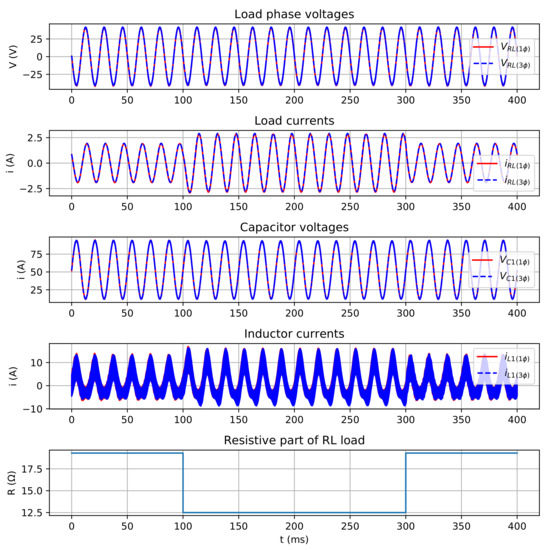
Figure 22.
Waveforms during the transient period.
In accordance with Figure 22, the capacitor and load phase voltages remain constant during this transition. The changing in the load and inductor currents is noticed when the load impedance changes its value. This behavior is expected, once the electrical current is inversely proportional to the impedance. The simulations show that with a little change in the load impedance, even the inverter running in open-loop, there is no disturbance in the output voltage inverter for both models. This allows for the conclusion that the single-phase proposed model is able to represent the dynamic behavior of the state variables even in transient loads.
5. Experimental Results
In order to support the simulation results of the proposed single-phase model, a three-phase Buck-Boost inverter prototype was performed as shown in Figure 23. The same values as indicated in Table 1 were implemented at the prototype for all cases analyzed. The duty cycle ratio is calculated at each step time of 50 s in accordance with Equation (32).
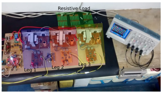
Figure 23.
Prototype with resistive load.
5.1. R Load
The main experimental results are shown in Figure 24a,b and Figure 25a,b in which the system operates under constant 18 resistive load. Table 5 shows the electrical quantities for the simulated single-phase and three-phase prototype.
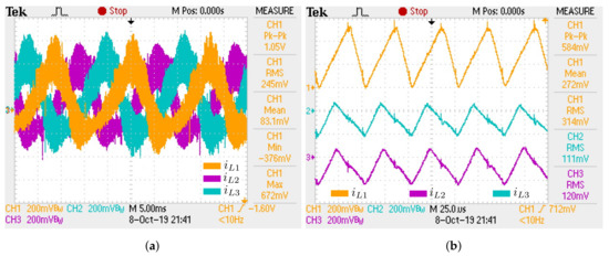
Figure 24.
Experimental inductor waveforms for R load case: (a) Inductor currents (25A/V); (b) Details
of inductor currents (25A/V).
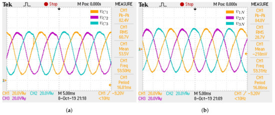
Figure 25.
Experimental waveforms of capacitor and load phase voltages for R load case: (a) Capacitor
voltages; (b) Load phase voltages.
Table 5.
Comparisons between simulated results of single-phase model with experimental results of three-phase model: R load.
The practical results validate the proposed single-phase equivalent circuit and space state model. In accordance with Table 5, the simulated and experimental results are quite similar. Small differences are expected due to the model not taking into account some non idealities, such as resistances and parasitic inductances present in a real circuit, as well as switching noises that can cause some voltage/current sparks in the waveforms. The maximum static gain obtained () was 2.67.
5.2. RL Load
In this case, an identical RL used in simulations presented in Section 4.2 is fed by inverter. The main experimental results are shown in Figure 26, Figure 27 and Figure 28 in which the system operates under constant load. Table 6 shows the electrical quantities for simulated single-phase and experimental three-phase prototype.
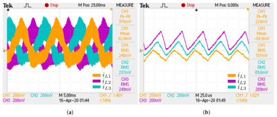
Figure 26.
Experimental inductor waveforms for RL load case: (a) Inductor currents (25A/V);
(b) Details of inductor currents (25A/V).
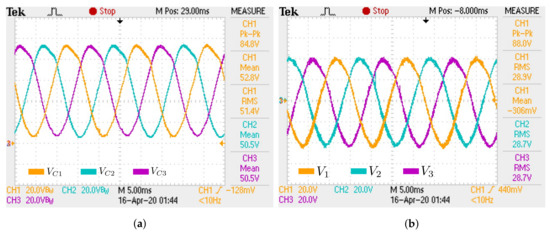
Figure 27.
Experimental waveforms of capacitor and load phase voltages for RL load case: (a) Capacitor
voltages; (b) Load phase voltages.
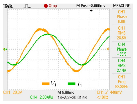
Figure 28.
Load voltage and current for phase 1: RL load.
Table 6.
Comparison between simulated results of a single-phase model with experimental results of the three-phase model: RL load.
These experimental results are in compliance with the simulations performed in Section 4.2. In accordance with Table 6, the simulated and experimental results for RL load are quite similar. It leads to the conclusion that the single-phase model can represent the dynamic behavior of three-phase models under inductive balanced loads with precision.
5.3. RC Load
In this scenario, an identical RC used in simulations presented in Section 4.3 is fed by inverter. The main experimental results are shown in Figure 29, Figure 30 and Figure 31 in which the system operates under a constant load. Table 7 shows the electrical quantities for the simulated single-phase and three-phase prototype.
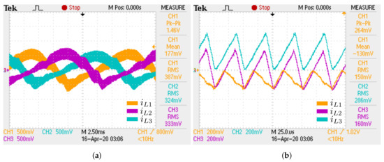
Figure 29.
Experimental inductor waveforms for RC load case: (a) Inductor currents (25A/V);
(b) Details of inductor currents (25A/V).
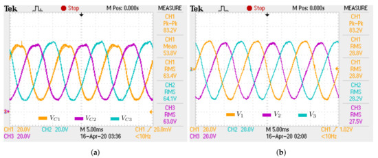
Figure 30.
Experimental waveforms of capacitor and load phase voltages for RC load case: (a) Capacitor
voltages; (b) Load phase voltages.
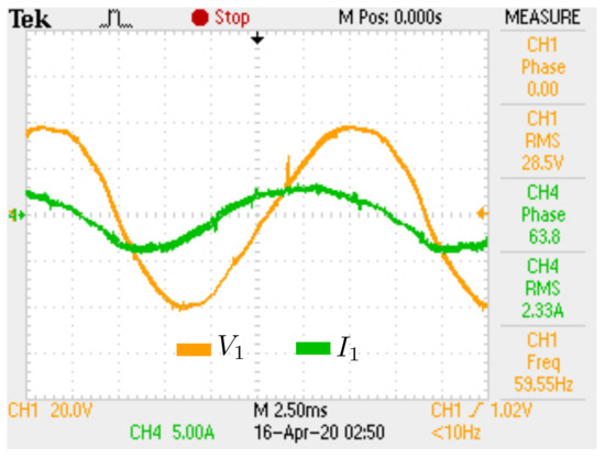
Figure 31.
Load voltage and current for phase 1: RC load.
Table 7.
Comparison between simulated results of single-phase model with experimental results of a three-phase model: RC load.
In this case, taking the values shown in Table 7, small differences can be observed between the simulated single-phase model and experimental results of the inverter. These differences are due to the capacitors used in the load are electrolytic capacitors. These type of capacitors have large leaking currents, which can cause some variations in capacitance values. These facts do not invalidate the proposed model.
5.4. RL Transition Load
The series RL load used in this experimental case has the same parameters described in Section 4.4. Initially, it was made by a 24.7 equivalent resistance with a 22.1 mH inductor. In the first transition, the resistive part of the RL load was decreased by 10 . The waveforms of RL load phase voltages and currents in the first transition are shown in Figure 32a and Figure 33a. The waveforms for inductor currents and capacitors voltages are shown in Figure 34a and Figure 35a, respectively. In the second transition, the resistive part of the RL load backs the original value. The waveforms for load phase voltage and current, inductor currents, and capacitor voltages for the second transition are shown in Figure 32b, Figure 33b, Figure 34b and Figure 35b.
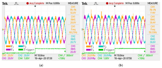
Figure 32.
Experimental load phase voltages for RL transition load case: (a) First transition; (b) Second
transition.
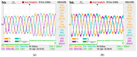
Figure 33.
Experimental load phase currents for RL transition load case: (a) First transition; (b) Second
transition.
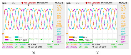
Figure 34.
Experimental capacitor voltages for RL transition load: (a) First transition; (b) Second
transition.
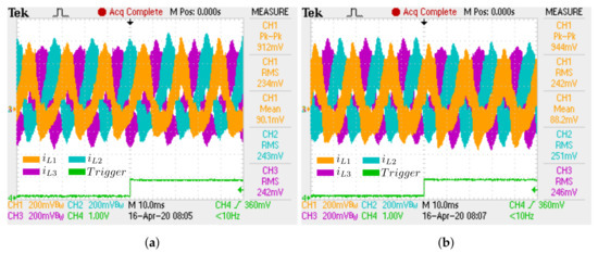
Figure 35.
Experimental Inductor currents for RL transition load: (a) First transition; (b) Second
transition.
Several different situations were performed in order to compare the single-phase model simulations with the real three-phase inverter. The experimental results are in compliance with simulation results presented in Section 4.4, and validate the applicability of the single-phase model to represent the full model inverter in steady state. Furthermore, it can be useful to design and calculate the inductance and capacitance of inverter inductors and capacitors.
6. Conclusions
This work has presented an equivalent single-phase circuit of a three-phase Buck-Boost inverter with balanced load for analysis and modeling purposes. In order to confirm the study results, a 200 W three-phase inverter prototype with several types of output load was implemented. The behavior in steady state of the simulated single-phase proposed model demonstrated that it can be used with property in order to obtain previous simulated results of the three-phase Buck-Boost inverter. The simulated and experimental results show clearly that the single-phase equivalent circuit can represent each leg of the three-phase Buck-Boost inverter model with exactness. Furthermore, its simulation demands less computer effort than the three-phase model. Thus, it is useful for a design of the inverter, predictive control strategy, or other techniques that are crucial for solving the model.
Author Contributions
V.M. conceived the idea. A.M. helped with micro-controller programming and writing the original draft preparation. W.S. made substantial contributions to conception, design, analysis, and experimental verification. W.S., J.F., and L.E. contributed to review and editing the final version. All authors have read and agreed to the published version of the manuscript.
Funding
This study was financed by the Fundação de Amparo à Pesquisa e Inovação do Espírito Santo (FAPES) – Finance Code 536/2018. The APC was funded by Fundação de Amparo à Pesquisa e Inovação do Espírito Santo.
Acknowledgments
This work has been supported by LEPAC (Laboratório de Eletrônica de Potência e Acionamentos Elétricos)-UFES, PPGEE (Postgraduate Program in Electrical Engineering)-UFES, Plexim for providing the PLECS Software licenses, Fundação de Amparo à Pesquisa e Inovação do Espírito Santo (FAPES), Coordenação de Aperfeiçoamento de Pessoal de Nível Superior—Brasil (CAPES), and the authors would like to thank Jordan Nachsin for supporting the writing review.
Conflicts of Interest
The authors declare no conflict of interest.
References
- Vallejos, W.D.P. Standalone photovoltaic system, using a single stage boost DC/AC power inverter controlled by a double loop control. In Proceedings of the 2017 IEEE PES Innovative Smart Grid Technologies Conference-Latin America (ISGT Latin America), Quito, Ecuador, 20–22 September 2017; pp. 1–6. [Google Scholar]
- Melo, F.C.; Garcia, L.S.; de Freitas, L.C.; Coelho, E.A.A.; Farias, V.J.; de Freitas, L.C.G. Proposal of a Photovoltaic AC-Module With a Single-Stage Transformerless Grid-Connected Boost Microinverter. IEEE Trans. Ind. Electron. 2018, 65, 2289–2301. [Google Scholar] [CrossRef]
- Huang, Q.; Ma, Q.; Huang, A.Q. Single-phase dual-mode four-switch Buck-Boost Transformerless PV inverter with inherent leakage current elimination. In Proceedings of the 2018 IEEE Applied Power Electronics Conference and Exposition (APEC), San Antonio, TX, USA, 4–8 March 2018; pp. 3211–3217. [Google Scholar]
- Radwan, H.; Sayed, M.A.; Takeshita, T.; Elbaset, A.A.; Shabib, G. A novel single-stage high-frequency boost inverter for PV grid-tie applications. In Proceedings of the 2018 IEEE Applied Power Electronics Conference and Exposition (APEC), San Antonio, TX, USA, 4–8 March 2018; pp. 2417–2423. [Google Scholar]
- Sevilmiş, F.; Karaca, H. Real time control of the inverter using TM320F28335 DSP with Matlab Simulink. In Proceedings of the International Conference on Engineering Technologies (ICENTE)-Konya/TURKEY, Konya, Turkey, 7–9 December 2017. [Google Scholar]
- Cárceres, R.O.; Garcia, W.M.; Camacho, O.M. A Buck-Boost DC-AC converter: Operation, analysis and control. In Proceedings of the 6th IEEE Power Electronics Congress. CIEP 98 (Cat. No.98TH8375), Morelia, Mexico, 12–15 October 1998. [Google Scholar]
- Sarowara, G.; Choudhuryb, M.A.; Hoquea, A. A Novel Control Scheme for Buck-Boost DC to AC Converter for Variable Frequency Applications. Procedia-Soc. Behav. Sci. 2015, 195, 2511–2519. [Google Scholar] [CrossRef][Green Version]
- Rajendran, S.; Kumar, S.S. A Single Phase AC Grid Tied Solar Power Generation Using Boost DC–AC Inverter with Modified Non-Linear State Variable Structure Control. Available online: https://www.semanticscholar.org/paper/A-Single-Phase-AC-Grid-Tied-Solar-Power-Generation-Rajendran-Kumar/184eddb2c9c8830927bf4fa78f95691d9724bf8c (accessed on 21 March 2020).
- Mansour, A.S.; Osheba, D.S.M. Performance of a Single-Stage Buck-Boost Inverter Fed from a Photovoltaic Source Under Different Meteorological Conditions. In Proceedings of the 2019 21st International Middle East Power Systems Conference (MEPCON), Cairo, Egypt, 17–19 December 2019. [Google Scholar]
- Sreekanth, T.; Lakshminarasamma, N.; Mishra, M.K. A Single Stage Grid Connected High Gain Buck-Boost Inverter with Maximum Power Point Tracking. IEEE Trans. Energy Convers. 2017, 32, 330–339. [Google Scholar] [CrossRef]
- Shafeeque, K.M.; Subadhra, P.R. A Novel Single-Phase Single-Stage Inverter for Solar Applications. In Proceedings of the 2013 Third International Conference on Advances in Computing and Communications, Cochin, India, 29–31 August 2013; pp. 343–346. [Google Scholar]
- Sasidharan, N.; Singh, J.G. A Novel Single Stage Single Phase Reconfigurable Inverter Topology for a Solar Powered Hybrid AC/DC Home. IEEE Trans. Ind. Electron. 2017, 64, 2820–2828. [Google Scholar] [CrossRef]
- Yalçin, F.; Himmelstoss, F.A. A New 3-Phase Buck-Boost AC Voltage Regulator. Electr. Power Compon. Syst. 2016, 44, 2338–2351. [Google Scholar] [CrossRef]
- Li, X.; Yan, Z.; Gao, Y.; Qi, H. The Research of Three-phase Boost/Buck-boost DC-AC Inverter. Energy Power Eng. 2013, 5, 906–913. [Google Scholar] [CrossRef]
- Antivachis, M.; Bortis, D.; Schrittwieser, L.; Kolar, J.W. Three-phase buck-boost Y-inverter with wide DC input voltage range. In Proceedings of the 2018 IEEE Applied Power Electronics Conference and Exposition (APEC), San Antonio, TX, USA, 4–8 March 2018; pp. 1492–1499. [Google Scholar]
- Husev, O.; Matiushkin, O.; Roncero-Clemente, C.; Vinnikov, D.; Chopyk, V. Bidirectional Twisted Single-Stage Single-Phase Buck-Boost DC-AC Converter. Energies 2019, 12, 3505. [Google Scholar] [CrossRef]
- Gu, L.; Zhu, W. Single-stage high-frequency-isolated three-phase four-leg buck–boost inverter with unbalanced load. IET Power Electron. 2020, 13, 23–31. [Google Scholar] [CrossRef]
© 2020 by the authors. Licensee MDPI, Basel, Switzerland. This article is an open access article distributed under the terms and conditions of the Creative Commons Attribution (CC BY) license (http://creativecommons.org/licenses/by/4.0/).