Abstract
In this letter, a compact dual-mode bandpass filter (BPF) with an ultra-wide stopband that employs two folded open-loop resonators (FOLRs) and stub-loaded resonators (SLRs) is proposed. The dual-mode resonators are optimized by loading two SLRs onto the folded open-loop resonators, and this process is analyzed using the dual-mode theory. To miniaturize the device size and increase chip performance, the proposed BPF is fabricated by a III–V compound semiconductor-fabrication process using a high-performance GaAs substrate based on the integration passivation device (IPD) fabrication process. A compact dual-mode BPF with low insertion loss and high return loss is designed and fabricated. Two extra transmission zeros (TZs) located in the high-frequency range increase the wide stopband, and the two TZs near the passband result in a higher selectivity. A resonant frequency centered at 7.45 GHz with an insertion loss of −1.21 dB and a measured return loss of higher than −23.53 dB and 3 dB fractional bandwidths of 5.8% are achieved. The stopband can be suppressed up to 20 GHz owing to the two tunable TZs resulting in higher selectivity and wideband rejection. The size of the filter was drastically optimized using a simplified architecture of two FOLRs and SLRs.
1. Introduction
The rapid development in current wireless-communication systems has resulted in remarkable challenges and demands for high performance, low-cost, and high-yield microwave devices, such as filters, couplers, power dividers, and balanced-to-unbalanced (balun). In particular, dual-band filters have become key components in dual-band microwave devices. To meet the demand, dual-mode bandpass filters (BPFs) have become attractive components in modern communication systems [1,2,3,4,5,6]. Until today, BPFs have been produced and fabricated using Teflon-based printed circuit boards (PCBs) [7,8], low-temperature co-fired ceramic (LTCC) [9,10], silicon-based semiconductor-fabrication technology [11], and so on [12,13,14]. Compared with PCBs, the LTCC and silicon-based semiconductor-fabrication techniques offer more advantages in terms of high integration and miniaturization. However, all these approaches suffer defects, such as high substrate loss, low accuracy, and difficult integration with systems.
In particular, BPFs serve as an important component in microwave systems to reject out-of-band noise from the system and environment. The fabrication accuracy of a critical dimension significantly affects the center frequency and out-of-band response of a BPF. The GaAs substrate-based integration passivation device (IPD) fabrication process has become one of the best approaches to meet these challenges of modern radio-frequency (RF) components, modules, and systems owing to its excellent performance in terms of high-quality factor, high self-resonant frequency, small size, low substrate loss, and so on [15,16]. A thick-metal fabrication process based on the IPD fabrication approach was developed for this proposed dual mode BPF design. The fabrication-process details are introduced in the Results and Discussion.
In this study, a dual-mode BPF is proposed, simulated, and fabricated using stub-loaded resonators (SLRs) consisting of a folded open-loop resonator (FOLR) and a center-loaded stub. Zhang first demonstrated that stub-loaded open-loop resonators can be used for a dual-band BPF design owing to the dual-mode resonators [17]. However, in this dual-mode BPF design, the even-mode resonator was designed with a high-frequency stopband to realize an ultrabroad out-of-band suppression of up to 20 GHz. Two tunable extra transmission zeros (TZs) can be shifted by changing the impedance of the designed even-mode resonator and the coupling between adjacent SLRs. Based on the above description, modified SLRs are introduced to design a dual-mode BPF with ultra-high out-of-band suppression using a high-performance GaAs-based IPD fabrication process. The flowchart of the designed BPF is shown in Figure 1.
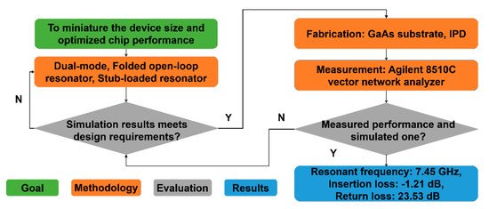
Figure 1.
The flowchart of the proposed bandpass filter (BPF), including the goal, methodology, evaluation, and results.
2. Filter Design and Theoretical Analysis
The topological structure of the proposed dual-mode SLR is shown in Figure 2, which consists of a pair of dual-mode SLRs including folded open loop resonators with an open stub and a pair of 50 Ω input/output feed lines. Because the SLR is located at the middle of the open-loop resonator, odd and even-mode analyses can be used to explain its characteristics because of this symmetrical structure. Based on the dual-mode theory, the equivalent circuits of the proposed SLR under odd and even-mode excitations are shown in Figure 2b,c.
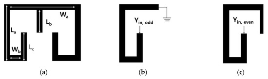
Figure 2.
Layout of the proposed (a) dual-mode folded open-loop and stub-loaded resonators (SLRs). (b) Odd-mode equivalent circuit. (c) Even-mode equivalent circuit.
For the odd-mode excitation, because of the electric wall at the middle of the open-loop resonator, the circuit will act as a shorted circuit in the SLRs. Therefore, the resonant frequency (fodd) can be expressed as Equation (1) [18].
where c is the speed of light in free space and εeff represents the effective dielectric constant of the substrate, and the symbols La, Lc, Wa, Wb in Equation (1) are related to Figure 2a. We observe that fodd is only determined using the outer length of the folded open-loop resonator. Figure 2a shows that the proposed SLRs are electrically shorted from the simulated current density during the odd-mode operation, which verifies the abovementioned phenomenon.
For the even-mode excitation, a magnetic wall exists along the center of the open-loop resonator, and no current flows across the center. Thus, an open circuit exists, as shown in Figure 2c. From the simulated current-density result (Figure 3b), we can also observe a very low current density at the symmetrical plane of the proposed folded open loop with SLRs. Therefore, the resonant frequency (feven) can be expressed as Equation (2).
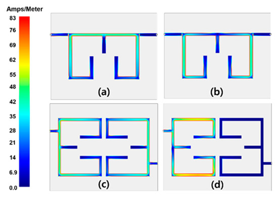
Figure 3.
Current density of proposed resonator and BPF at different resonant frequencies: (a) and (c) 7.45 GHz (odd-mode), (b) and (d) 13.92 GHz (even-mode).
Compared with Equation (1), it can be found that the length of the SLR (Lb) related to Figure 2a significantly affects the tunable BPF design and can separately shift the even-mode response; however, it does not influence the odd mode resonant frequency. In this designed BPF, we also utilize two tunable TZs in the high-frequency range by changing the even-mode resonant response.
Figure 3 shows the current densities at different resonant frequencies simulated using the Sonnet EM simulation tool. Figure 3c,d shows that the odd and even-mode excitations of the proposed BPF are similar to those shown in Figure 3a,b, respectively. Under the odd-mode operation, because of the electric wall, the introduced SLRs are electrically shorted, and the current densities of the SLRs are relatively low at both the right and left sides, as shown in Figure 3c.
However, under the even-mode operation, a magnetic wall exists along the center of the symmetric plane; almost all of the current is concentrated on the proposed folded open-loop resonators and SLRs; and a null current density at the center part of the open-loop resonator can also be observed, as shown in Figure 3d. Simultaneously, the right part of the modified open-loop resonator also shows a voltage null; thus, all the input signals are isolated in this even-mode operation. As a result, the even-mode resonance of the proposed FOLR and SLRs can be optimized to increase the out-of-band suppression at a higher frequency to realize a wide stopband. The designed BPF based on the proposed SLR consists of two symmetrical folded open-loop resonators, SLRs, and input/output feed lines, as shown in Figure 4a. The RF response of the proposed BPF is simulated using full-wave electromagnetic (EM) Sonnet software and measured by an Agilent 8510C vector network analyzer (VNA). The detailed layer information of the fabricated BPF is shown in Figure 4b. The fabricated BPF chip is connected to the PCB using Au wire-bonding technique. To minimize the effect of the Teflon substrate, negligible vias are made in the blank parts of the Teflon substrate and connected to the large aluminum ground, as shown in Figure 4c. The top and 3D-views of the fabricated BPF are shown in Figure 4d.
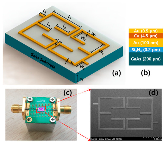
Figure 4.
Proposed dual-mode BPF with folded open-loop resonators (FOLRs) and SLRs. (a) 3D schematic view of the BPF layout. (b) Layer information of fabricated BPF. (c) Picture of fabricated BPF on PCB with Al ground for measurement and (d) scanning electron microscopy (SEM) images of the fabricated BPF.
Figure 5a shows that the resonant frequency of the designed BPF can be shifted by length L3 corresponding to Equation (1). Meanwhile, the location of third TZ is also shifted obviously. Consequently, the length of L3 is fixed to 900 µm with a center frequency of 7.45 GHz. In our previous study, the 3-dB fractional bandwidth (FBW) was determined using an external quality factor (Qe), which is related to the position of the input/output feed lines [1].
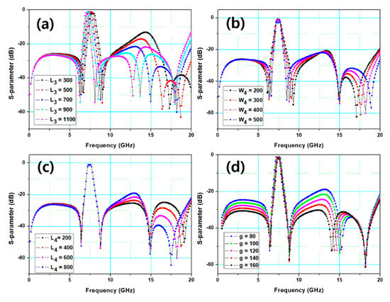
Figure 5.
Simulated results of the proposed dual-mode BPF for different (a) L3, (b) W4, (c) L4, and (d) g parameters.
As the distance of the feed line (W4) increases from 200 to 500 µm, the FBW value continues to decrease, indicating that Qe continued to increase as shown in Figure 5b. The bigger Qe is, the higher is the BPF selectivity and the closer the first and second TZs become. Moreover, the fourth TZ is also shifted to a higher frequency to achieve a wider stopband. Although the height distance of the feed line can modify Qe, the fourth TZ is also simultaneously shifted. Nevertheless, the SLR length can only shift the fourth TZ by itself, as shown in Figure 5c. When the SLR length changes from 200 to 800 µm, the fourth TZ is shifted from 19.15 to 15.93 GHz, which implies that the response of the even-mode resonator can effectively shift the fourth TZ to realize a wide out-of-band suppression. Even though the fourth TZ is shifted to a lower frequency, the suppression level increases, and a trade-off exists in optimized parameter L4. In this study, we modify the traditional even-mode operation from a bandpass type to realize a bandstop type using a folded open-loop resonator. Hence, the second resonant frequency is transferred to the bandstop response to increase the out-of-band suppression. Figure 5d shows that as the gap (g) between two adjacent folded open-loop resonators increases from 80 to 160 µm, the third TZ is shifted to a low frequency from 15.26 to 14.03 GHz, and the return loss decreases from 18.92 to 30.19 dB; however, the other TZs are not affected. In conclusion, optimized parameters L3, W4, L4, and g are fixed as 700, 400, 600, and 100 µm, respectively.
3. Results and Discussion
The proposed BPF was fabricated on a high-performance, low-loss, 6-in GaAs substrate with a relative permittivity of 12.85 and loss tangent of 0.006 using an advanced III–V compound semiconductor fabrication process, as shown in Figure 6. The fabrication started with wafer cleaning using acetone/isopropanol/deionized water for 5 min/1 min/3 min, respectively, to remove residues from the substrate. Then, a 200-nm-thick Si3N4 passivation layer was deposited by plasma-enhanced chemical vapor deposition (PECVD). The relative permittivity and loss tangent of the PECVD- deposited Si3N4 layer were 7.5 and 0.002, respectively. These values could increase the breakdown voltage and reduce the leakage current as well as improve the adhesion between the substrate and the first metal layer. Next, a thin Ti/Au seed metal with a thickness of 20/80 nm was deposited by DC sputtering, following electroplating mask patterning using a standard photoresist lithography process. A thick metal layer of Cu/Au (4.5 µm/0.5 µm) was deposited using the electroplating process. Then, the photoresist mask was stripped by a lift-off process and the undesired seed metal was removed by reactive-ion etching to achieve chip isolation. Finally, the GaAs substrate was polished to 200 µm and diced to separate the devices.
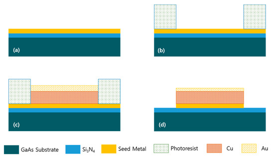
Figure 6.
Schematics of the proposed BPF device fabrication. (a) Wafer passivation of 200 nm thick Si3N4 deposited by PECVD and 100 nm thick gold seed metal deposited by sputtering. (b) Plating mask lithography and development. (c) Cu/Au (4.5 µm/ 0.5 µm) metallization by plating. (d) Removal of photoresist by lift-off and seed metal dry etching for chip isolation.
The 3D schematic and the cross-sectional view of the finally fabricated BPF are shown in Figure 4a. The detailed dimensions are as follows: L1 = 1600 µm, L2 = 300 µm, L3 = 700 µm, L4 = 600 µm, W1 = 100 µm, W2 = 500 µm, W3 = 850 µm, W4 = 400 µm, t1 = 10 µm, t2 = 200 µm, and g = 100 µm. The total chip size is 3.3 × 2.0 mm2. Figure 4c shows that the fabricated BPF on the GaAs substrate was connected to the input and output connectors via 50 Ω impedance-matching transmission lines on the designed PCB using die-attaching and gold wire-bonding techniques. The RF performance was measured and characterized using the Agilent 8510C VNA.
Figure 7 shows the simulated and measured S-parameters of the proposed BPF with an open-loop resonator and SLR. A high performance BPF is achieved with ultra-high out-of-band suppression using SLR. The center frequency of the measured results was located at 7.45 GHz with a low insertion loss of −1.21 dB, a return loss of −23.53 dB, and a 3-dB FBW of 5.8%. Four TZs are located at 6.42, 8.72, 15.26, and 17.97 GHz with attenuation levels of −50.33, −53.66, 62.66, and −55.32 dB, respectively. The measured RF performance shows a good agreement with the simulated one, thereby verifying the proposed design concept and the advanced III–V compound semiconductor-fabrication processes. The reasons for the slight difference between the measurement and simulation results could be attributed to the lack of an accurate connection among the connectors because of the manual soldering of the PCB input and output matching lines [19]. Table 1 compares ours to similar reported designs, which also proves the superior merits of this proposed BPF chip.
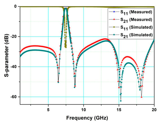
Figure 7.
Simulated and measured results of the proposed BPF with stub-loaded folded open-loop resonators.

Table 1.
Comparisons to other similar fabricated designs.
4. Conclusions
In this study, a FOLR with SLRs has been researched for a dual mode BPF based on even and odd-mode operations. This BPF was designed, simulated, and fabricated using high-performance GaAs-based IPD fabrication with two SLRs and center-loaded resonators. The passband of the measured results resonated at 7.45 GHz with a low insertion loss of −1.21 dB and an FBW of 5.8%. The four TZs were located at 6.42, 8.72, 15.03, and 18.26. Four tunable TZs shifted by the modified open-loop resonator and the even-mode resonator of the SLRs increased the high-frequency suppression up to 20 GHz, resulting in higher selectivity and wideband rejection. The characteristics of the dual-mode stub-loaded open-loop resonator were investigated to modify the extra TZs to realize high performance BPFs. Furthermore, the measured results showed a very good agreement with the simulated results. This proposed BPF with an ultra-wide stopband, which has significant design flexibility, compact topological structure, and high selectivity, could be an attractive candidate for RF systems.
Author Contributions
Conceptualization, Z.Y., E.S.K. and N.Y.K.; methodology, W.Z.; software, J.Z.; validation, W.Z.; formal analysis, W.Z., J.Z.; investigation, W.Z.; resources, W.Z.; data curation, W.Z.; writing—original draft preparation, W.Z.; writing—review and editing, Z.Y., E.S.K. and N.Y.K.; visualization, Z.Y.; supervision, Z.Y., E.S.K. and N.Y.K.; project administration, Z.Y.; funding acquisition, Z.Y. All authors have read and agreed to the published version of the manuscript.
Funding
This research was funded by the National Natural Science Foundation of China, grant number 61904092; the Shandong Provincial Natural Science Foundation of China, grant number ZR2018BF027; and the Project of Shandong Province Higher Educational Science and Technology Program, grant number J18KA382. This research was also partially supported by the Basic Science Research Program through the National Research Foundation of Korea (NRF) funded by the Ministry of Education (No. 2018RlA6AlA03025242 and No. 2018R1D1AIA09083353) and was also supported by a Research Grant of Kwangwoon University in 2020.
Conflicts of Interest
The authors declare no conflict of interest.
Abbreviation
The following abbreviations are used in this manuscript:
| BPF | Bandpass filter |
| EM | Electromagnetic |
| FOLR | Folded open-loop resonator |
| FBW | Fractional bandwidth |
| IPD | Integration passivation device |
| LTCC | Low-temperature co-fired ceramic |
| PCBs | Printed circuit boards |
| PECVD | Plasma-enhanced chemical vapor deposition |
| RF | Radio-frequency |
| SEM | Scanning electron microscopy |
| SLRs | Stub-loaded resonators |
| TZs | Transmission zeros |
| VNA | Vector network analyzer |
References
- Yao, Z.; Wang, C.; Kim, N.Y. A compact dual-mode dual-band bandpass filter using stepped-impedance open-loop resonators and center-loaded resonators. Microw. Opt. Technol. Lett. 2013, 55, 3000–3005. [Google Scholar] [CrossRef]
- Liu, Q.; Zhou, D.; Lv, D.; Zhang, D.; Zhang, J.; Zhang, Y. Multi-layered dual-mode substrate integrated waveguide bandpass filter with input and output ports located on same substrate layer. IET Microw. Antennas Propag. 2019, 13, 2641–2648. [Google Scholar] [CrossRef]
- Deng, H.; Sun, L.; Xue, Y.; Liu, F.; Xu, T. High selectivity and common-modesuppression balanced bandpass filter with TM dual-mode SIW cavity. IET Microw. Antennas Propag. 2019, 13, 2129–2133. [Google Scholar] [CrossRef]
- Li, H.; Shao, C.; Tong, C.; Tang, H.; Chen, J. Miniaturised dual-mode dielectric resonator filter with controllable passband. Electron. Lett. 2020, 56, 235–236. [Google Scholar] [CrossRef]
- Chaudhury, S.S.; Awasthi, S.; Singh, R.K. Dual-mode bandpass filter based on substrate-integrated waveguide loaded with complementary split ring resonators. Microw. Opt. Technol. Lett. 2018, 60, 2639–2642. [Google Scholar] [CrossRef]
- Sedighi, S.; Maragheh, S.; Dousti, M.; Dolatshahi, M.; Ghalamkari, B. A dual-mode tunable bandpass filter for GSM, UMTS, WiFi, and WiMAX standards applications. Int. J. Circuit Theory Appl. 2019, 47, 561–571. [Google Scholar] [CrossRef]
- Tsai, L.C.; Huse, C.W. Dual-band bandpass filters using equal-length coupled-serial-shunted lines and Z-transform techniques. IEEE Trans. Microw. Theory Technol. 2004, 52, 1111–1117. [Google Scholar] [CrossRef]
- Chen, C.Y.; Hsu, C.Y. A simple and effective method for microstrip dual-band filters design. IEEE Microw. Wirel. Compon. Lett. 2006, 16, 246–248. [Google Scholar] [CrossRef]
- Yeung, L.K.; Wu, K.L. A compact second-order LTCC bandpass filter with two finite transmission zeros. IEEE Trans. Microw. Theory Technol. 2003, 51, 337–341. [Google Scholar] [CrossRef]
- Xu, J.X.; Zhang, X.Y.; Zhao, X.L.; Xue, Q. Synthesis and implementation of LTCC bandpass filter with harmonic suppression. IEEE Trans. Compon. Packag. Manuf. Technol. 2016, 6, 596–604. [Google Scholar] [CrossRef]
- Wang, S.; Chang, R.H. 2.4 GHz CMOS bandpass filter using active transmission line. Electron. Lett. 2016, 52, 371–372. [Google Scholar] [CrossRef]
- Suresh, L.N.; Manickam, B. Multiple cascode flipped active inductor-based tunable bandpass filter for fully integrated RF front-end. IET Circuits Device Syst. 2020, 14, 93–99. [Google Scholar] [CrossRef]
- Huang, J.; Li, J.N.; Yang, Y.; Li, J.; Li, J.H.; Zhang, Y.T.; Yao, J.Q. Active controllable bandwidth of THz metamaterial bandpass filter based on vanadium dioxide. Opt. Commun. 2020, 465, 125616. [Google Scholar] [CrossRef]
- Shi, Y.R.; Zhang, J.Z.; Zhou, M.; Feng, W.J.; Cao, B.L.; Che, W.Q. Miniaturized W-band gap waveguide bandpass filter using the MEMS technique for both waveguide and surface mounted packaging. IEEE Trans. Circuits II 2019, 66, 938–942. [Google Scholar] [CrossRef]
- Wu, Y.; Qiang, T.; Wang, C.; Adhikari, K.K.; Lv, X.; Wu, Y. GaAs-Based IPD-Fabricated center-frequency-controllable bandpass filter with asymmetrical differential inductor and air-bridge enhanced capacitor. IEEE Access 2019, 7, 137784–137793. [Google Scholar] [CrossRef]
- Liu, L.; Kuo, S.; Abrokwah, J.; Ray, M.; Maurer, D.; Miller, M. Compact harmonic filter design and fabrication using IPD technology. IEEE Trans. Compon. Pack. Technol. 2007, 30, 556–562. [Google Scholar]
- Zhang, X.Y.; Quan, X. Novel centrally loaded resonators and their applications to bandpass filters. IEEE Trans. Microw. Theory Tech. 2008, 56, 913–921. [Google Scholar] [CrossRef]
- Hong, J.S.; Lancaster, M.J. Microstrip Filters for RF/Microwave Applications; Wiley: New York, NY, USA, 2004. [Google Scholar]
- Liang, J.G.; Wang, C.; Kim, N.Y. Dual-band ultra-wideband bandpass filter with eight-resonant modes and quad-transmission zeros employing synchronous-quasi-resonance. Radioengineering 2017, 26, 713–720. [Google Scholar] [CrossRef]
- Zheng, T.; Xu, G.W.; Luo, L. High performance suspended spiral inductor and band-pass filter by wafer level packaging technology. Microsyst. Technol. 2017, 23, 10–1007. [Google Scholar] [CrossRef]
- Huang, C.H.; Lin, Y.C.; Horng, T.S.; Hwang, L.T. Design of compact bandpass filter using transformer-based coupled resonator on integrated passive device glass substrate. In Proceedings of the Asia-Pacific Microwave Conference 2011, Melbourne, VIC, Australia, 5–8 December 2011. [Google Scholar]
- Tseng, Y.C.; Ma, T.G. On-chip GIPD bandpass filter using synthesized stepped impedance resonators. IEEE Microw. Wirel. Compon. Lett. 2014, 24, 140–142. [Google Scholar] [CrossRef]
- Chen, J.H. Enhancement of 5 GHz on-chip bandpass filter performance by using CMOS-MEMS inductors. Microsyst. Technol. 2018, 24, 2371–2377. [Google Scholar] [CrossRef]
© 2020 by the authors. Licensee MDPI, Basel, Switzerland. This article is an open access article distributed under the terms and conditions of the Creative Commons Attribution (CC BY) license (http://creativecommons.org/licenses/by/4.0/).