Article

Characterization Circuit, Gate Driver and Fixture for Wide-Bandgap Power Semiconductor Device Testing

Department of Energy Engineering, German Jordanian University, Amman 11180, Jordan
*
Author to whom correspondence should be addressed.
Electronics 2020, 9(5), 703; https://doi.org/10.3390/electronics9050703
Submission received: 11 April 2020 / Revised: 19 April 2020 / Accepted: 22 April 2020 / Published: 25 April 2020
(This article belongs to the Section Semiconductor Devices)

Abstract

:
The world is currently experiencing major advancement in the electrification of both the industrial and commercial sectors. This is part of an effort to reduce reliance on combustible fuels, reduce emissions, integrate renewable energy systems and increase efficiency. Due to the complexity of modern circuits and systems, any circuit’s design should start with proper simulation and device selection, to reduce overall cost and time of prototyping, both of which require accurate and thorough device characterization. Wide bandgap (WBG) power semiconductor devices offer superior characteristics over conventional devices, including faster switching speeds, higher breakdown voltage, lower losses, and higher operating temperature. These properties call for special test circuits and procedures for accurate characterization. In this work, custom characterization circuits and fixtures, suitable for WBG devices are designed, tested, and described. The circuits measure several of the main characteristics of voltage controlled WBG power switches. Different technology devices were tested and characterized.

1. Introduction

With the advancements of power electronics and their applications, demand is rising to use devices with higher voltages, smaller footprints, and lower energy consumption. This is especially true for wide-bandgap (WBG) semiconductor devices, which offer superior characteristics over conventional devices, including faster switching, higher breakdown voltage, lower losses, and higher operating temperature [1,2,3,4].
It is very important to fully understand a device’s behavior before using it in a circuit design. Certain device characteristics are very important in the design process. Such characteristics include blocking voltage, leakage current, on-state resistance, turn-on, and turn-off times.
Manufacturers go through a detailed process in developing data sheets using device characteristics, but only under certain operating conditions. However, when pushing a device to its operating limits, circuit designers may prefer to actually characterize the device at different operating conditions, better related to desired operation. The properties of WBG devices require special test beds and procedures to accurately characterize such devices [5].
The authors in [6] discuss some of the common PCB parasitic considerations. This paper focuses on cross talk and I-V alignment issues that are introduced by using chokes for current measurement. In terms of characterization, they only discussed the switching waveforms, and testing was performed on bare-die devices, not on commercial packages where different parasitics exist.
The authors in [7] propose an alternative circuit for switching characterization, in an attempt to achieve better control over testing parameters over a double pulse test circuit (DPT). This work is only concerned with dynamic on-state resistance characterization of 200 V GaN devices.
The authors in [8] compared GaN on-state resistance under hard- and soft-switching conditions for two types of GaN devices and one Si device. The authors discuss DPT testing considerations and introduce a new design for a clamping circuit. Testing however, was exclusive to the dynamic on-state resistance of GaN devices, and there was no discussion of other characterization capabilities. A DPT was built for SiC device switching characterization at different load conditions in [9], however, measurement hardware was not presented. The authors in [10] propose an active gate driver design for cross talk suppression. This reference mainly discusses the gate driver, and not the entire test bed or characterization process.
The authors in [11] characterize a SiC switch for comparison with a Si switch using a DPT. The paper focuses on comparing the device’s performance for an EV powertrain application, rather than the characterization process or the developed hardware.
A novel gate driver design that suppresses switching overcurrent and overvoltage in SiC MOSFETs is presented in [12]. The gate driver features variable voltage and gate resistance, which yields good results in suppressing the switching oscillations. The authors used a DPT-based test bed to evaluate the gate driver performance, but only discuss switching characteristics. The gate driver output is connected to the MOSFET using relatively long leads, which may contribute to the gate loop parasitic inductance, effecting the acquired measurement. The authors in [13] discuss and review clamping circuits for dynamic on-state resistance characterization, and propose a new clamping circuit design. This reference only discusses the clamping aspect of the WBG device’s characterization.
SiC MOSFETs offer the ability to work at higher voltage levels and frequency, but this can introduce unwanted side effects, such as the self-sustained oscillations, which might unintentionally turn on the gate driver. The authors in [14] experimentally investigate this phenomenon using a DPT-based test bed. This paper experimentally validates the importance of minimizing the gate and power loop parasitic inductance, to suppress the oscillations, but without hardware description or design.
In this paper, a low-parasitic, high-speed gate driver, a double pulse test circuit, and a low noise leakage current test fixture are designed, built, and tested. The proposed circuits and procedures are unique to what is available in the literature as they provide a comprehensive characterization solution for blocking, switching, and on state measurements. In addition, complete hardware design and layout is described in detail.
The article is organized as follows: Section 2.1 describes the gate driver circuit design, Section 2.2 describes the double pulse tester circuit design and testing considerations, and Section 2.3 describes the leakage current testing fixture. The test results are in Section 3.

2. Materials and Methods

2.1. Low-Parasitic, High Speed Gate Driver

Driving WBG devices requires a fast and capable gate driver circuit. The function of the gate driver in power electronic circuits is to isolate the logic and control portions of the circuit from the power path, in addition to providing the device with the proper turn-on and turn-off voltages or currents. For example, a control logic level of 1, or an analog voltage level of 5 V used to turn on a SiC MOSFET, must produce a 15 V differential voltage between the gate and the source terminals of the MOSFET; while a turn-off signal will require a −3 V differential between the same terminals. It is important to note that in many power electronic circuits the source terminal of the switch is most likely floating, which requires a floating differential gate drive output.
At the same time, the gate driver circuit should not affect or slow down the device’s operation. This requires special attention to the parasitic gate loop inductance, which may cause delayed switching, ringing, and even cause the switch to unintentionally turn-on, which may result in the destruction of the switch.
To minimize the gate loop area, and maximize the flexibly of the testing bed, a modular design approach was followed. The gate driver circuit board was separated from the main test board, which allowed changing the gate driver board easily to perform tests at different gate voltages. A schematic of the gate driver circuit is shown in Figure 1.
The gate driver circuit consisted of two main components, the gate driver IC, and the DC/DC converter. The gate driver IC’s main job was to receive the switching logic signal from the controller and output a similar shaped signal, while providing isolation between the logic side and the power side. The most important characteristics of a gate driver IC are its switching capabilities and its common mode transient immunity (CMTI) [6]. The Silicon Labs si8271 GB gate driver IC was selected for this design, as it provided sufficient current, high switching speed, and very high CMTI of over 200 kV/μs. Another reason for selecting this IC was its separate pull-up/down outputs, which allowed controlling of the turn-on and turn-off slew rates with minimal external components, thus minimizing the gate loop parasitics and achieving a sharper gate driving signal. The slew rate could be controlled by changing the output resistors, which is a thin-film of low ESL resistors with the smallest possible package footprint to minimize the gate loop inductance.
The DC/DC converter provides two main functions. It supplies the appropriate high and low voltages to the gate driver IC, and provides galvanic isolation between the power side of the gate driver circuit and any external circuitry. The RECOM R15P21503D 2 W isolated DC/DC converter was selected for this research. This converter outputs +15 V and −3 V, and provides 6.4 kVDC of voltage isolation. Four decoupling capacitors were used to filter noise and voltage ripple.
The gate drives were designed on a separate PCB. The gate driver board can be directly soldered to the DUT’s gate and source pins, as close to the package as possible, forming a Kelvin connection with the source pin. This approach minimized the loop area by bypassing the long leads of the DUT, and sharing the least length with the power loop. A 0.8 mm 2-layer board was used, reducing the gate loop area at a reasonable price. The gate driver PCB layout can be seen in Figure 2 and the populated board soldered to the DUT in Figure 3.

2.2. Double Pulse Test Circuit

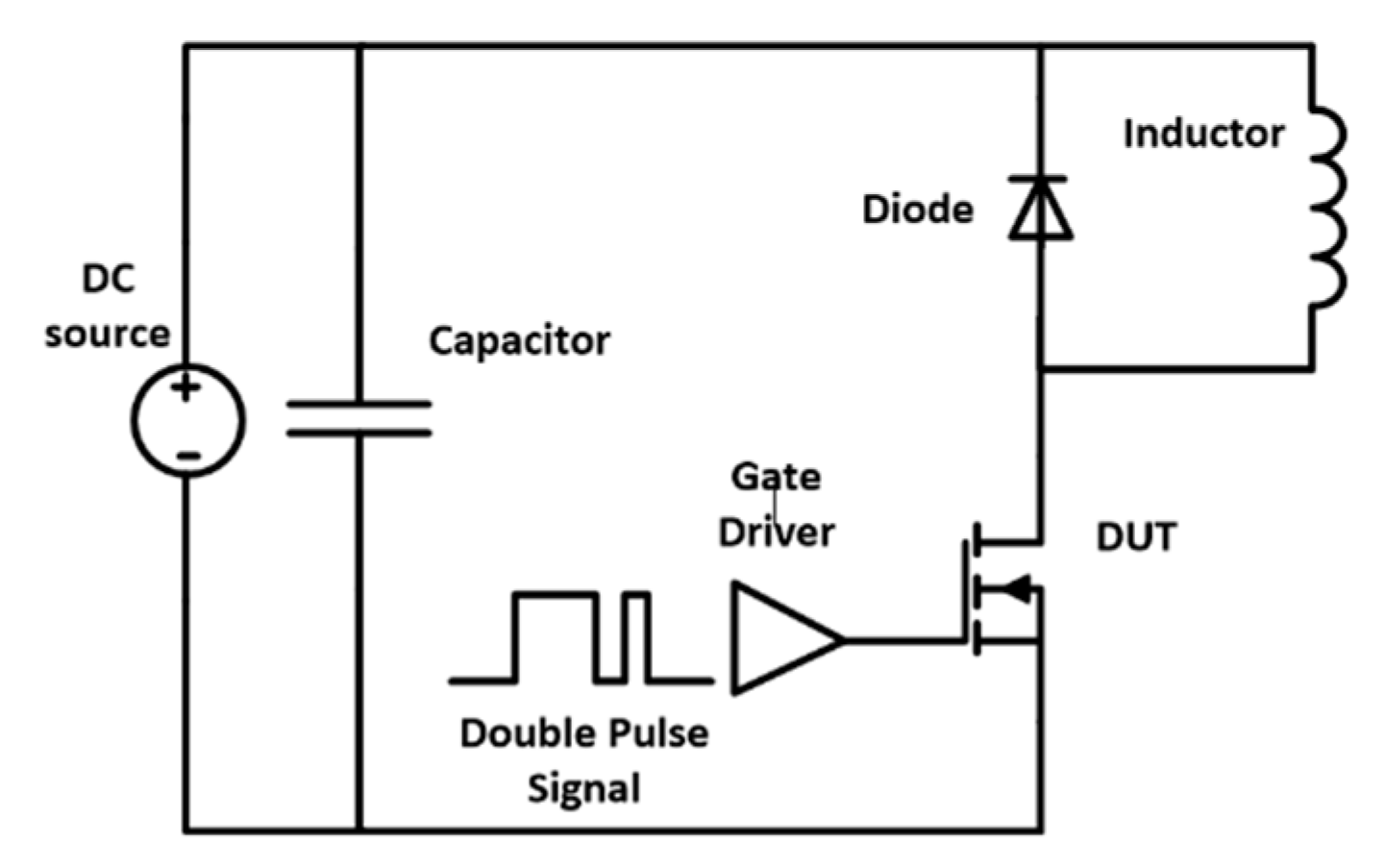
The double pulse method is widely used in industry to test power semiconductor devices, and to evaluate their dynamic performance. As the name suggests, two pulses are sent to the device under test (DUT). By regulating the DC bus voltage and the first pulse’s duration, the DUT’s dynamic characteristics can be evaluated under any desired I-V condition. A typical double pulse tester circuit is shown in Figure 4.
A pulse is first applied to the DUT, closing the circuit, and charging the inductor. Since the inductor will gradually allow more current to flow, the longer the duration of the pulse, the higher the current flowing through the circuit. When the desired testing current is reached the pulse ends, and the switch turns off. This will capture the turn-off characteristics of the switch at the applied voltage and current.
The gate signal is kept low for a long enough duration for all the transients to reach steady state. Next, a second pulse is applied and the DUT is turned on. This captures the turn-on characteristics under the same voltage and current. The pulse is kept high long enough to reach a steady state, then the signal goes low to turn off the DUT and to allow the inductor to discharge through the freewheeling diode. Using a high inductive load, the current magnitude change between the two pulses would be small, and may be neglected, and since the two pulses happen in a short amount of time, the DUT temperature is not affected [9,15]. A typical DPT waveform is shown in Figure 5.
Although the main principle of the DPT is not complicated, designing a DPT to characterize WBG devices is a challenging task. The main challenge was to build a test bed that would allow the capture of the actual device performance, and not the effects of the test bed parasitics. As WBG devices operate at both higher frequency and higher power than conventional devices, the influence of parasitics may entirely conceal the actual performance of the DUT.
An equivalent circuit showing the parasitic elements existing in a DPT is illustrated in Figure 6. There are mainly seven parasitic elements in the DPT: Lds, Cds, and Cd in the power loop, Lgs and Cgs in the gate loop, and Lcm and Cgd shared by both loops. The main issues caused by these parasitic elements are power loop ringing and overshoot voltages, which cause electromagnetic interference and reliability issues. The biggest contributors to these issues are the power loop inductance Lds and the diode capacitance Cd [6,16].
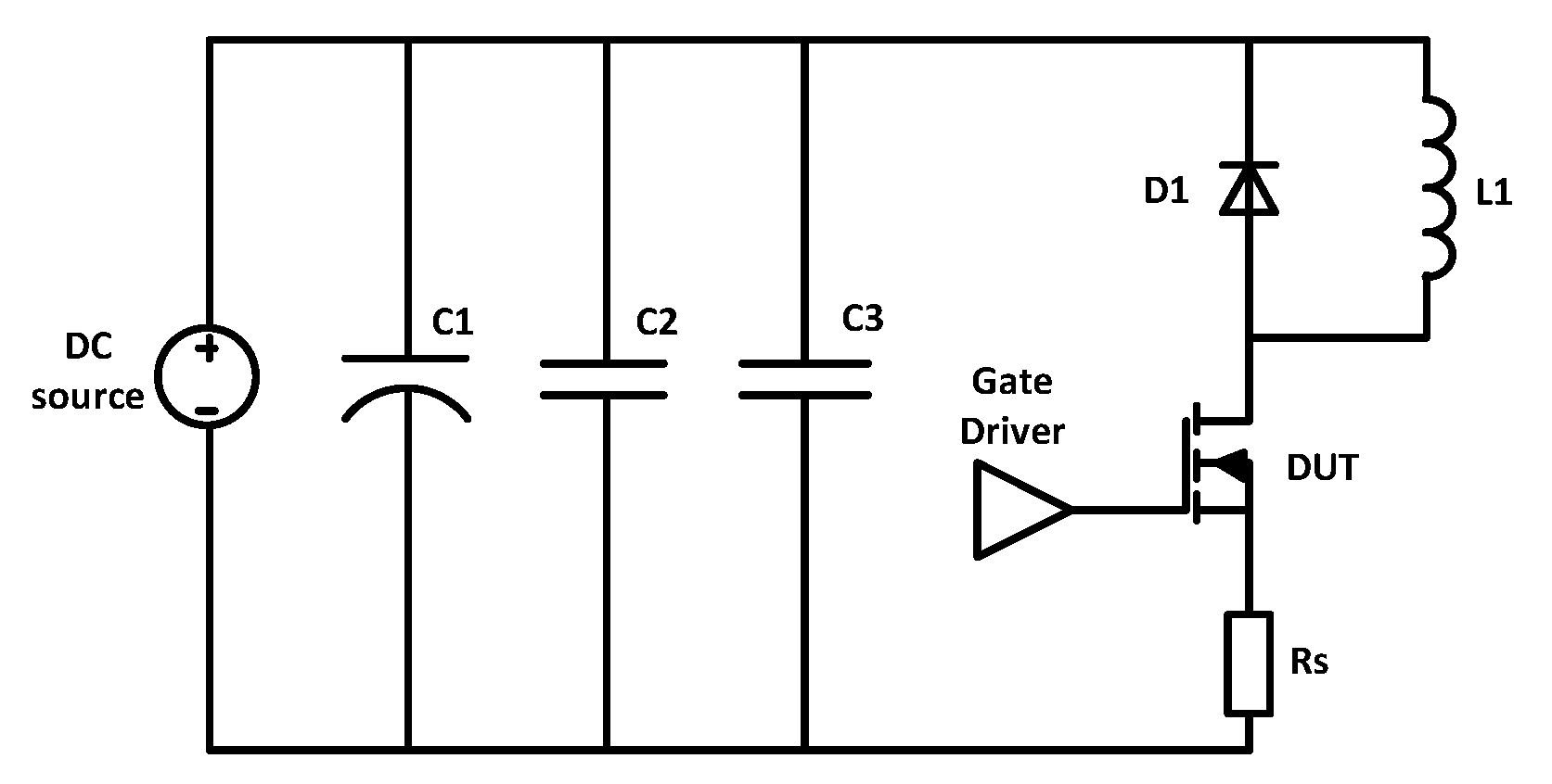
Components’ size, type, and packaging should be carefully selected for the DPT to work properly, while achieving minimal parasitics. The DPT schematic used is shown in Figure 7.
The load inductor is not only responsible for establishing the current during the test, but also to maintain near constant current between the two pulses. Thus, it should be large enough to maintain the current for the desired off-time. The load inductor value is determined under worst case conditions, which occur under maximum voltage and minimum current.
Another critical property of the inductor is its core saturation point. If the core saturates before reaching the testing current the inductance will collapse, resulting in a very rapid current increase and could potentially destroy the DUT. To reach the target inductance while achieving a high saturation current level, Kool Mµ toroidal cores were used to build a custom inductor core.
To minimize the equivalent series resistance (ESR) of the inductor, 6 mm2 Litz wire was used. To minimize the equivalent parallel capacitance (EPC), the inductor was constructed using one layer of winding. The inductor was evaluated using a GW Instek 817 LCR meter to measure the inductance, and a saturation current tester to test the core’s saturation point. The final inductor had an inductance of 810 μH, and saturated at 80 A.
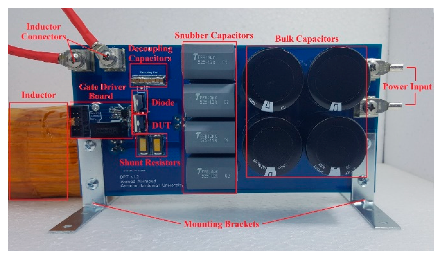
A DC capacitor bank (C1) was used to supply the inductor current, and it is designed to limit the voltage variation during the charging of the inductor. The capacitor should be designed to handle the maximum operating voltage, and the value should be determined under worst conditions, which occurs under minimum voltage and maximum current. It is preferred they are either electrolytic or film capacitors [6]. A capacitor bank was formed using four 560 μF 400 V electrolytic capacitors, with two connected in series, and then the two sets connected in parallel to form a 1060 μF 800 V capacitor bank.
A second stage made of film capacitors (C2) was added between the bulk capacitor bank and the decoupling capacitors to absorb or supply any high voltage or current spikes that are too fast for the electrolytic capacitors, and too demanding for the decoupling capacitors. Four 525 V 10 μF (FFB46J0106K) film capacitors arranged in parallel were empirically found to achieve high decoupling from the DC source, and enable the testing board to achieve much higher testing currents, with no noticeable voltage ripple.
Ceramic decoupling capacitors (C3) were used to supply transient current and mitigate overvoltage during the switching transient. To ensure good decoupling, seven 22 nF 1.5 kV (C1210 × 223KFRACTU) ceramic capacitors where used. The high voltage ratings ensure that the capacitors can withstand any possible voltage spikes during testing. To minimize the power loop parasitic inductance, the capacitors were chosen to have very low ESL ratings, and a wider 1210 footprint.
The freewheeling diode should be able to withstand the maximum testing current, be able to handle the testing voltage and voltage overshoots. Furthermore, it should have the fastest recovery time possible to minimize interference with the DUT’s performance evaluation. A diode with a low capacitance will reduce the overshoots caused by the parasitic second order oscillation. The diode chosen is a CREE C4D08120A SiC Schottky diode. SiC Schottky diodes have no reverse recovery time, and thus will insure no interference with DUT performance.
A shunt resistor (Rs) is used to measure the DUT’s current. As a shunt resistor, it must have very tight tolerance and low temperature coefficient. To minimize the power loop inductance, the resistors material must have low ESL. Two 100 mΩ (WSR5R1000FEA) power metal resistors were connected in parallel to form a 50 mΩ current sense resistor. These resistors have a low TRC, and a very low ESL. Using two parallel resistors instead of one further reduces the ESL and reduces the effect on the power loop inductance.
When designing test circuits, it is very important to place test points throughout the design, to ease data acquisition. With the DPT, waveforms give the most insight, and therefore a 500 MHz Teledyne LeCroy Wavesurfer oscilloscope and 500 MHz passive probes were used.
The instruments used are only the first step in acquiring good measurements. The probe setup and connection method has a major role in acquiring clean waveforms. Low inductance connection termination to the board is absolutely necessary. Probing a circuit always introduces some parasitics, which could potentially affect both the circuit and the measurement acquired, particularly when dealing with WBG devices.
Using a probe with a long ground lead such as in Figure 8a will introduce very high parasitic inductance, causing ringing in the measured waveform [6]. A better option is to use a short ground lead, as in the spring ground lead of Figure 8b, which introduces much less parasitic inductance and less background noise. However, it still picks up noise, and it does not provide a secure way to connect the probe to the circuit.
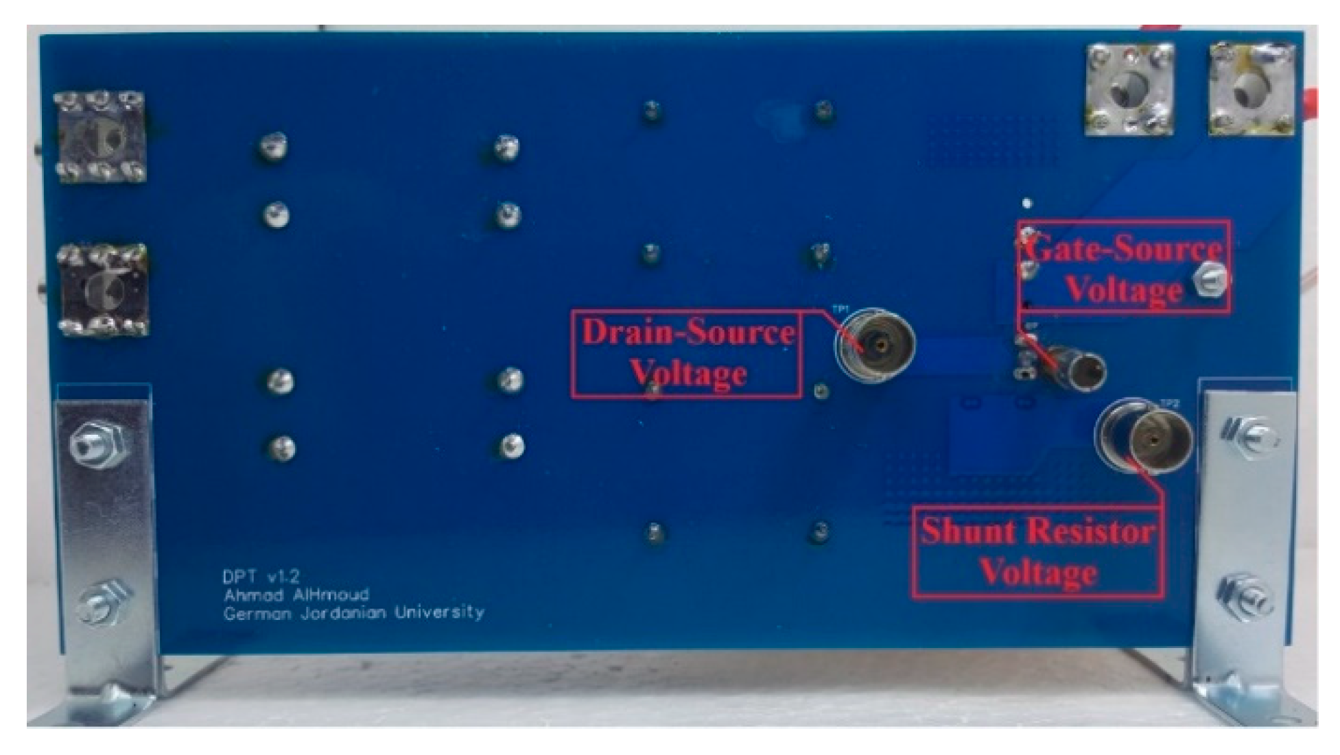
The best termination method is to use a PCB mounted shielded connecter as can be seen in Figure 9. This method provides the lowest measurement loop area, thus minimizing parasitic inductance and provides shielding all the way to the PCB board. Using this termination method provides the best probing results. In our design, the probes are perpendicular to the PCB board, and connected on the backside. This will shielded the probes behind the ground plane of the PCB, which will minimize any noise from the high current pulses during testing.
The PCB layout is a major contributor in minimizing parasitics, and achieving accurate test results [6]. The most critical aspect of the PCB layout is to minimize the power loop area. Conventional lateral power loop routing is based on placing all the components and traces on one side of the PCB as tightly as possible. It provides the ability to use single sided PCBs, but does not provide the minimal loop area, and lacks good field self-cancelation. The better approach is to use a vertical power loop routing scheme, where the top layer is used for the positive power path, and the bottom layer is used as a ground return path. This approach results in smaller power loop area and provides field self-cancelation because the current returns in a parallel trace to the positive flow [17,18].
However, conventional 1.6 mm double-sided PCBs are too thick to achieve substantially better results than the lateral approach, since the PCB thickness heavily affects the loop area and the field self-cancelation [17,18]. Using thinner PCBs is impractical as the board becomes too flexible and could potentially cause damage to solder joints, especially to surface mounted devices (SMD) components.
To minimize the distance between the positive plane and the ground plane while maintaining board strength, a 4-layer design approach is used. Four-layer PCBs can be built to have the top and first inner layer close to each other (typically 0.1 to 0.2 mm apart), which reduces the inductance dramatically, not only due to the reduced loop area, but also due to field self-canceling [17,18], as can be seen in Figure 10. A 4-layer PCB can be made thick enough to maintain the board’s structural integrity, while the additional two layers can be used to route shielded Kelvin connections for optimal signal integrity and measurement accuracy.
The top side of the populated DPT test board is shown in Figure 11, and the backside showing the probe connections in Figure 12.

2.3. Leakage Current Testing Fixtures

Forward blocking voltage or drain-source breakdown voltage is defined as the maximum voltage that the device is guaranteed to block between drain and source [19], and is usually linked to reaching a certain level of drain-source leakage current. Drain-source leakage current or drain cut-off current is defined as the leakage current that occurs when a voltage is applied across the drain and source with the gate and source short-circuited [19].
Datasheets usually use the rated voltage of the switch as the blocking voltage value, without including the upper limits of the switch, or the way it approaches the breakdown point, and often, they do not specify the basis on which the breakdown voltage value is chosen. Measuring forward leakage current enables extraction of the forward blocking voltage of a switch, since the blocking voltage is characterized by a certain level of increase in forward leakage current.
Drain-source leakage current values are often specified to be below a certain maximum level, but without including the exact value or profile of the leakage current change with the applied voltage. This makes it often very hard to compare devices based on their leakage current or provide accurate estimation of energy loss. The required test bed must perform two main functions: to be able to measure low currents down to the pA range, and to be able to test devices with voltages up to 1000 V.
A Keysight B2901A source/meter unit (SMU) is selected as the current measurement unit. This SMU is capable of measuring current as low as 100 fA, is able to perform voltage sweeps up to 42 V, and log measured data.
A major limitation of using SMUs is their relatively limited voltage range for this particular application. The SMU used in this work can only deliver up to 42 V, which is far below the sought range. This requires the use of an external voltage source in order to measure the leakage current at voltages up to 1000 V.
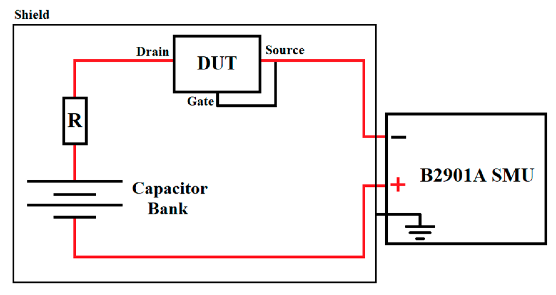
Ideally, adding a power source in series with the DUT, should solve the problem. Using a bench power supply causes too much noise in the voltage path, rendering the readings unusable. Any common mode noise may affect the readings as well. To overcome this issue, a capacitor bank was used as a non-switching, floating power supply, which provided a pure DC voltage with zero ripple, and no common mode issues with the SMU. This also enabled placing the entire capacitor bank inside a shield casing for complete noise shielding.
Since the leakage current is very small, the test will result in minor capacitor discharge. Six 800 µF 450 V electrolytic capacitors were used. Connecting three capacitors in series and two in parallel resulted in a 1600 µF 1350 V capacitor bank, which provided a large enough capacitance.
When using the sweep function of the SMU to generate a graph of the voltage–current relationship, the test may take some time. In this case, to increase the accuracy of the test, the capacitor voltage was measured before and after the test, and the voltage sweep values were compensated for the capacitor voltage decrease during the test by a linear approximation of the voltage drop, which was justified because of the very small voltage drop in comparison to the operating voltage.
If the DUT fails as a short, the SMU will see the full voltage of the capacitor bank. This is an issue as only 210 V is allowed at the inputs of the SMU. To protect the SMU from potential damage, a current limiting protection resistor was connected in series, therefore any catastrophic voltage drop would be across the resistor and not the SMU, if the DUT failed as a short. The resistor should not introduce measurement errors due to its relatively low value in comparison to the DUT. Figure 13 shows a schematic of the test setup, while Figure 14 shows the actual test circuit.
Dealing with very low currents, even probe insulation will leak enough current to potentially affect measurement that may overwhelm the actual DUT leakage current [20].
In order to prevent current leakage through the probe’s insulation, a special fixture was required. The fixture used a triaxial probe for the positive output, and a coaxial probe for the negative output. The probe used a guarding technique to eliminate leakage current from the measurement path. The guarding technique was based on surrounding the main conductor with a guarding shield that had the same potential of the main conductor, this would guarantee that no current would flow between them.
The guarding shield was further shielded with a grounding shield to block background noise. The negative probe was shielded with only one shield, which acted both as a guarding and a grounding shield [20], as illustrated in Figure 15.
The triaxial cable was built by wrapping a coaxial cable with a layer of aluminum foil, then covering it with a heat-shrink tube. The core of the coaxial cable would act as the main conductor, while the shield of the coaxial cable was terminated at the guard terminal of the SMU. The newly added layer would be used as the shield, and were terminated to the ground of the SMU. The probes were kept as short as possible to minimize parasitic capacitance, as shown in Figure 14.

3. Results

3.1. DPT Device Switching Test

To demonstrate the results of the test bed, two devices were tested under various testing conditions. SiC and GaN devices were chosen since they have similar voltage and current ratings and the same TO-220 package. Device information is shown in Table 1.
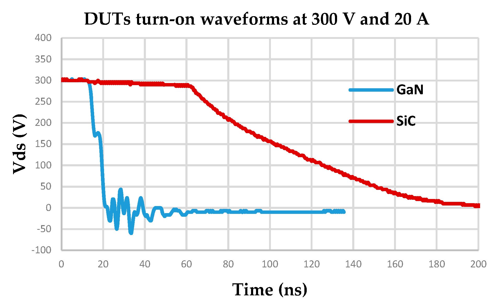
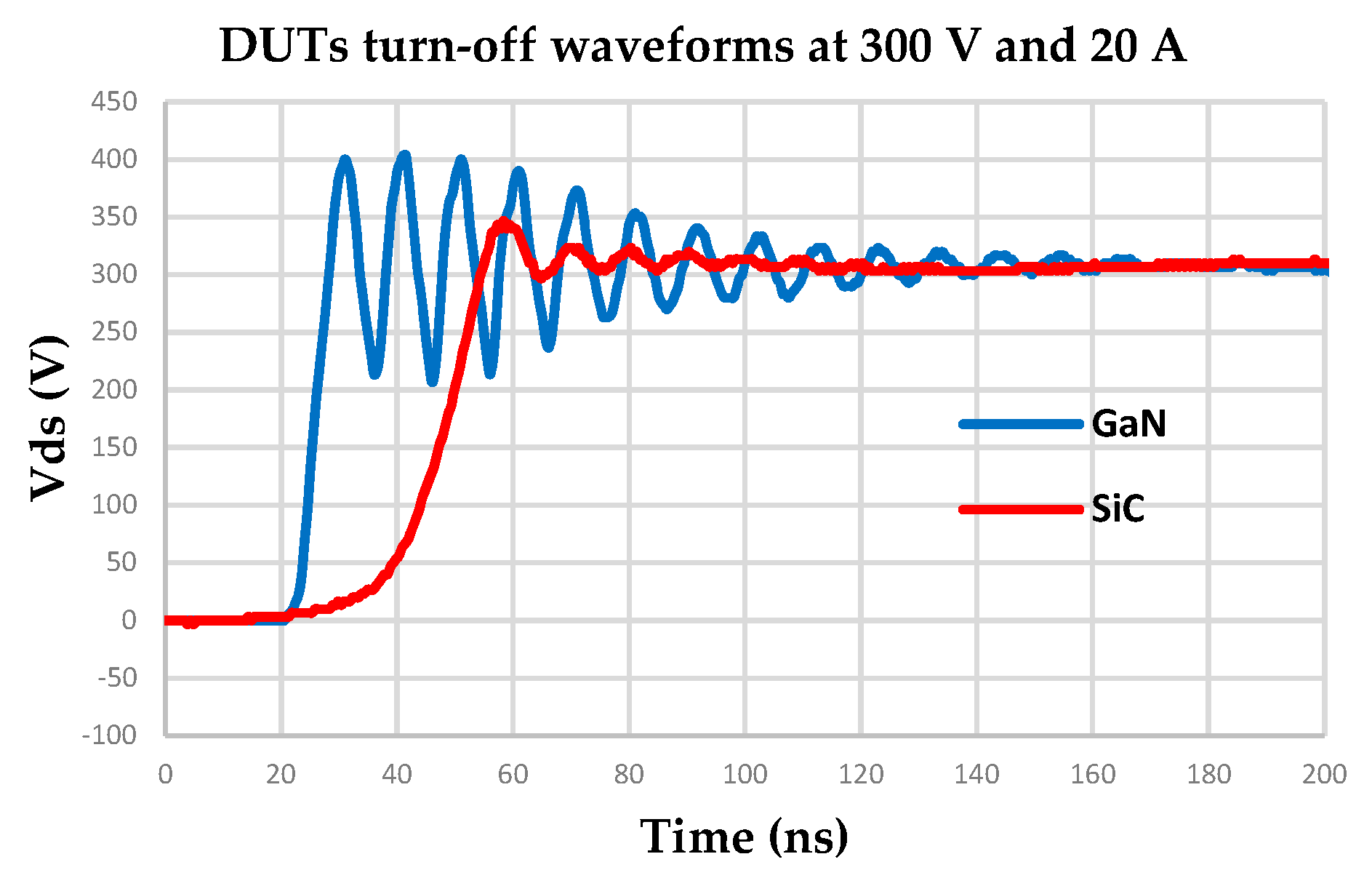
These devices were chosen, as they are commercially available at a reasonable price, and therefore more likely to be used first in applications. The 650 V class of semiconductor devices is widely used in electric drives, which may benefit from the advantages of WBG devices, and thus selected for this study. The two DUTs were tested with a 16.5 V gate turn-on voltage and −5 V gate turn-off voltage. Figure 16 and Figure 17 compares the turn-on and turn-off waveforms of the two devices, respectively.
As expected, the WBG devices have fast switching characteristics. For example, it can be seen in the above graphs that the GaN device has a voltage fall time of 15 ns (during turn-on) and voltage rise time of 10 ns (during turn-off). One of the main objectives of this research is to produce a test setup that captures the device’s actual performance, and not mask the characteristics due to the test setup limits. The test setup was able to accurately measure the waveforms and capture the device’s actual performance.

3.2. Shielded Low Current Fixture Test

To demonstrate the effectiveness of shielding on low current measurement, a low current measurement was conducted with and without the shielding as shown in Figure 18. This measurement was done in a normal room with no special electrical noise around, and the noise was high enough to significantly affect the measurement.

3.3. Blocking Test

A device’s breakdown is characterized by a sudden and rapid increase in forward leakage current. This test will demonstrate the test fixture capabilities to measure and characterize the forward leakage current and breakdown voltage. The devices used in this test are the Si and SiC MOSFETs detailed in Table 2. As can be seen from the table, the breakdown voltage is only given as a minimum value, while the leakage current is given only at the rated voltage and as a maximum limit.
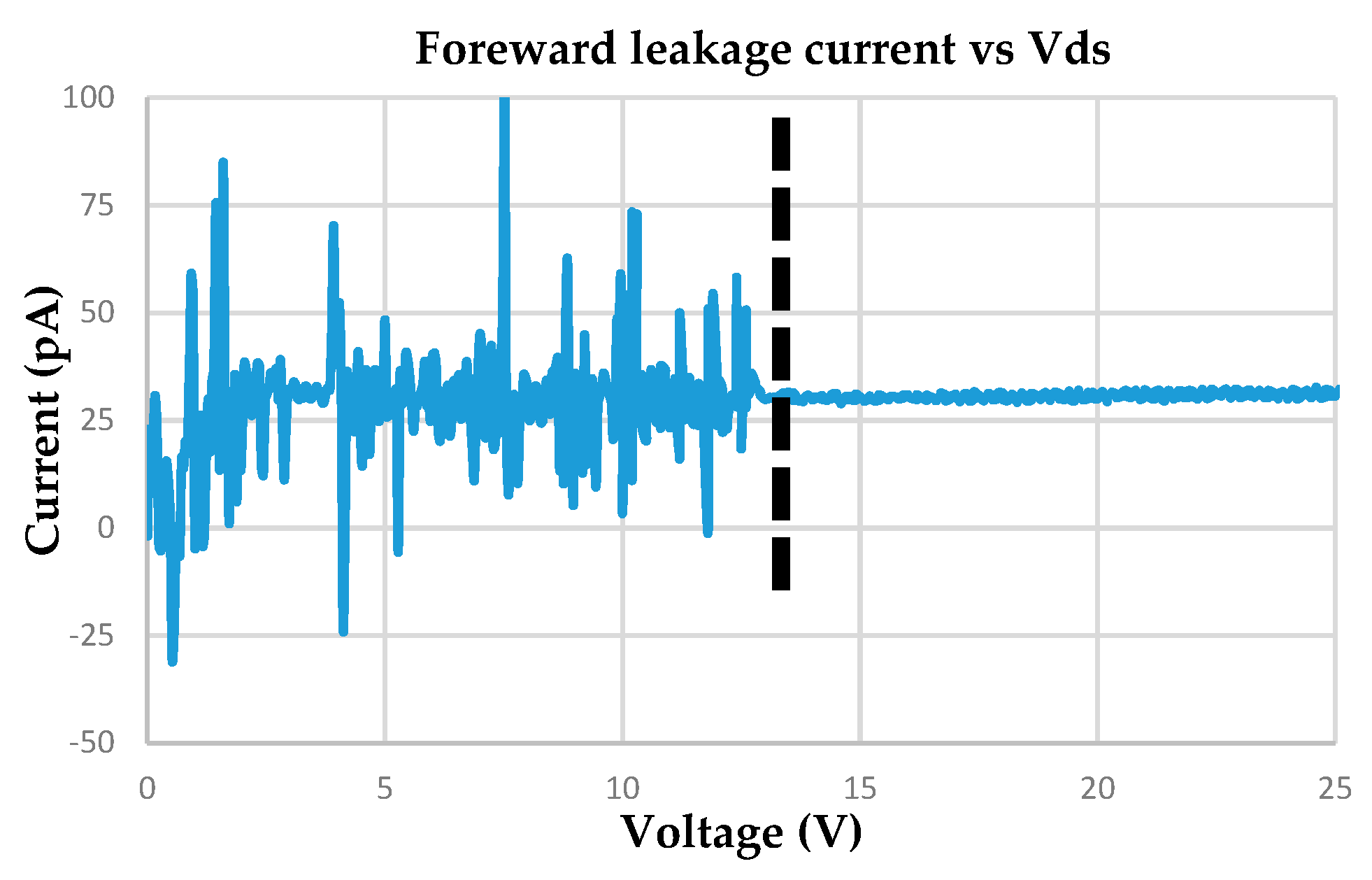
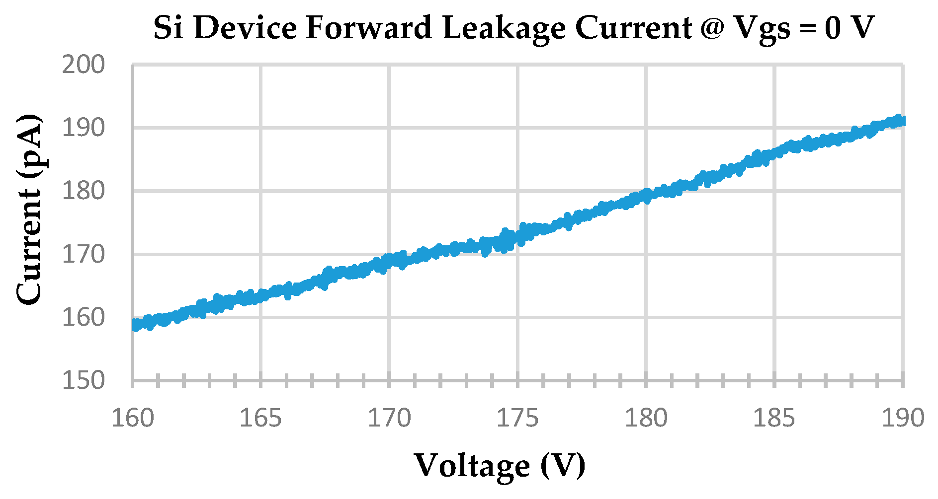
First, a leakage current test was performed on both devices, at a voltage range of 160–190 V to demonstrate the leakage current profile below the rated voltage. The results are shown in Figure 19 and Figure 20. Voltage was applied between the DUT’s drain and source, while the gate was shorted to the source terminal. This test demonstrates the capabilities of the fixture to provide accurate results at very low current levels.
To identify the blocking voltage of the DUTs, another test was performed, where the voltage is increased until the DUT breaks down. The test is stopped at a maximum voltage of 1030 V. Six 200 V, 12 kΩ resistors in series are used to limit the current to 16.7 mA at 1000 V.
The results of the test are shown in Figure 21 and Figure 22. There is no industry-standard leakage current value to specify that the device has reached breakdown, so no exact breakdown voltage will be specified. Instead, the leakage current profile should present more information about the way the device enters breakdown, and how fast it goes through it.
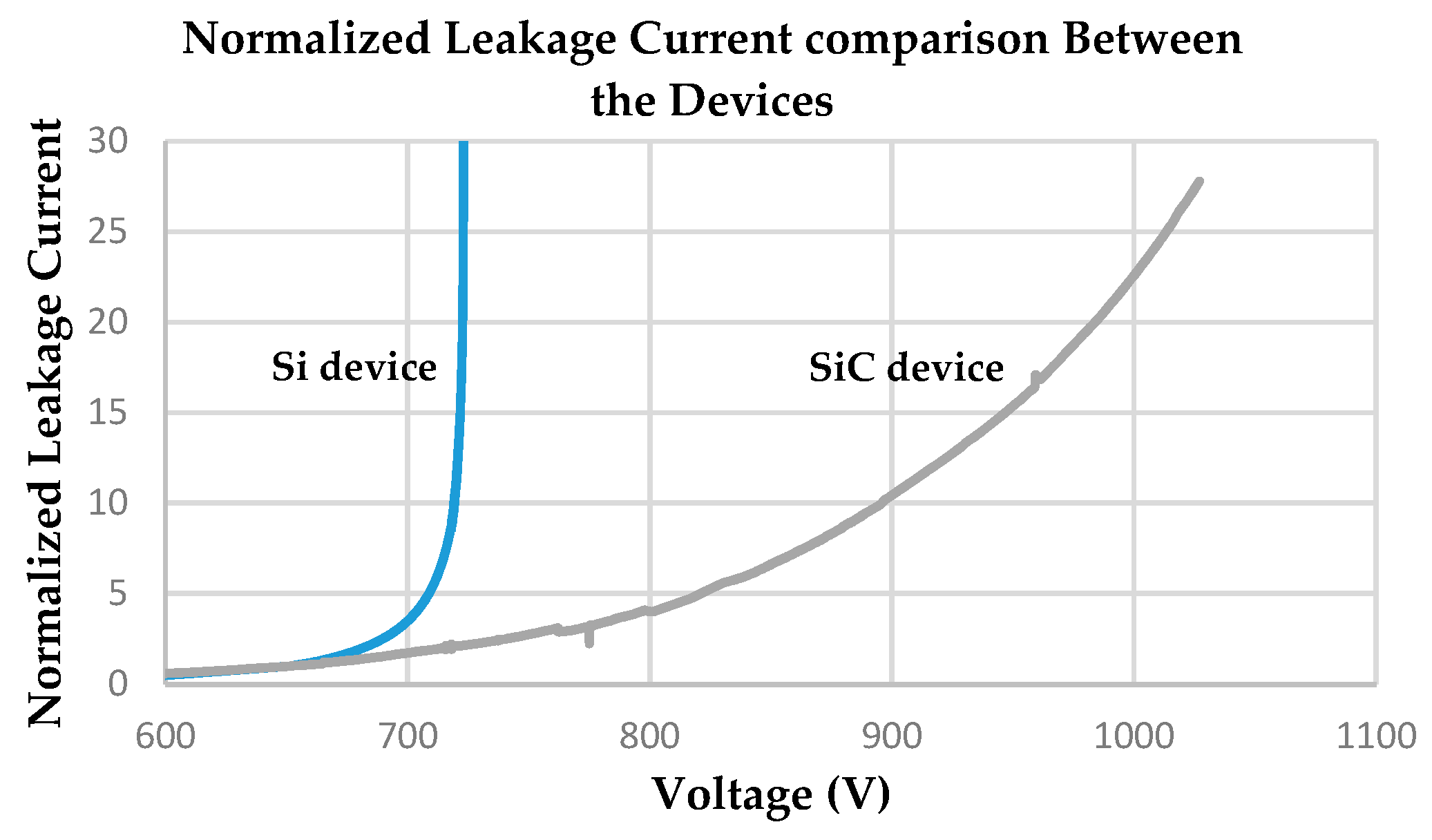
To better visualize the difference between the devices, the two curves were normalized to the leakage current value at the rated voltage (650 V), and plotted against each other, as can be seen in Figure 23.
Both DUTs are rated for 650 V, nevertheless, each of them reached higher voltages. The Si device only reached slightly higher voltage, breaking down at around 720 V, and showing a relatively sharp increase in leakage current beyond the rated voltage. On the other hand, the SiC demonstrated significantly higher breakdown voltage, showing an increase in current over a very wide range of applied voltage. These results show the significantly higher voltage withstanding capabilities for the WBG devices, and demonstrate how their behavior may differ greatly from the conventional Si device behavior.

4. Discussion

To be able to properly test a WBG device’s switching behavior it was necessary to build a gate driver and DPT board that eliminate as much parasitics as possible to acquire actual device performance. As explained above, detailed analysis of design parasitics was considered in the schematic circuit, circuit device elements, and PCB layout. In addition, a separate gate drive board was designed that is directly connected to the pins of the DUT. This resulted in reducing the logic signal path parasitics, while providing a four wire Kelvin connection for measurement. This greatly reduces the effect of the logic circuit on acquired waveforms.
The complete system was able to capture the switching behavior in the order of nanoseconds at higher voltage and current levels. This is extremely important information to capture, as it enables circuit designers to design their applications to operate at device limits. This also enhances the sizing and design of auxiliary circuits. Traditionally, with the lack of precise information, snubbers, filters, and voltage balancing networks were designed very conservatively, resulting in bulky more expensive systems. As shown in the Figure 16 and Figure 17, not only was the switching time obtained, but also the packaging related oscillations and ripple.
As most WBG power semiconductor devices only block in the reverse direction, it is often necessary to use a series diode for forward voltage blocking when applications require it. Doing so requires actual leakage current information to properly anticipate blocking voltage sharing across both devices, which may dictate diode device selection. As data sheets do not provide this information as shown in Table 2, it was necessary to design a leakage current fixture.
As shown in Figure 18, no meaningful information may be obtained at this low level of current, unless shielded probes are used. A low cost alternative to a triaxial cable is developed. In addition, a procedure to use a standard SMU with a capacitor bank is described, to obtain high precision leakage current at rated voltage. The designed fixture was able to capture leakage currents in the range of 100 fA, at rated voltage. This was only possible with careful design of the test leads, circuit schematic, shielding, housing, and supply.

Author Contributions

Conceptualization, O.S. and Z.D.; methodology, O.S.; software, Z.D. and A.A.-H.; validation, O.S., Z.D., and A.A.-H.; formal analysis, A.A.-H.; investigation, A.A.-H.; resources, O.S. and Z.D.; data curation, Z.D. and A.A.-H.; writing—original draft preparation, A.A.-H.; writing—review and editing, O.S. and Z.D.; visualization, A.A.-H.; supervision, O.S.; project administration, Z.D.; funding acquisition, Z.D. All authors have read and agreed to the published version of the manuscript.

Funding

This research received no external funding.

Acknowledgments

This work is supported by the deanship of scientific research at the German Jordanian University.

Conflicts of Interest

The authors declare no conflict of interest.

Abbreviations

The following abbreviations are used in this manuscript:
WBGWide bandgap
PCBPrinted circuit board
CMTICommon mode transient immunity
ICIntegrated circuit
DUTDevice under test
SMDSurface-mount devices
SMUSource/meter unit
VdsDrain-source voltage
RsShunt resistor
LdsDrain-source inductance
CdsDrain-source capacitance
CdDiode capacitance
LgsGate-source inductance
CgsGate-source capacitance
LcmCommon mode inductance
CgdGate-drain capacitance
ESREquivalent series resistance
EPCEquivalent parallel capacitance

References

  1. Saadeh, O. Modeling and Characterization of P-Type Silicon Carbide Gate Turn off Thyristors. Ph.D. Thesis, University of Arkansas, Fayetteville, AR, USA, 2011. [Google Scholar]
  2. Saadeh, O.S.; Mantooth, H.A.; Balda, J.C.; Agarwal, A.K.; Kashyap, A.S. The Modeling and Characterization of Silicon Carbide Thyristors. In Proceedings of the IEEE Power Electronics Specialists Conference (PESC), Rhodes, Greece, 6–10 October 2008; pp. 1092–1097. [Google Scholar]
  3. Richmond, J. An Overview of Cree Silicon Carbide Power Devices. In Proceedings of the Power Electronics in Transportation, Novi, MI, USA, 21–22 October 2004; pp. 37–42. [Google Scholar]
  4. Boutros, K.; Chu, R.; Hughes, B. Recent Advances in GaN Power Electronics. In Proceedings of the IEEE 2013 Custom Integrated Circuits Conference, San Jose, CA, USA, 22–25 September 2013; pp. 1–4. [Google Scholar]
  5. Ong, A. Characterization of Silicon Carbide Junction Field Effect Transistors and Metal Oxide Semiconductor Field Effect Transistors. Ph.D. Thesis, MSEE, University of Arkansas, Fayetteville, AR, USA, 2007. [Google Scholar]
  6. Zhang, Z.; Guo, B.; Wang, F.F.; Jones, E.A.; Tolbert, L.M.; Blalock, B.J. Methodology for Wide Band-Gap Device Dynamic Characterization. IEEE Trans. Power Electron. 2017, 32, 9307–9318. [Google Scholar] [CrossRef]
  7. Foulkes, T.; Modeer, T.; Robert, C.; Pilawa-Podgurski, N. Developing a standardized method for measuring and quantifying dynamic on-state resistance via a survey of low voltage GaN HEMTs. In Proceedings of the 2018 IEEE Applied Power Electronics Conference and Exposition, San Antonio, TX, USA, 4–8 March 2018; pp. 2717–2724. [Google Scholar]
  8. Li, R.; Wu, X.; Yang, S.; Sheng, K. Dynamic On-state Resistance Test and Evaluation of GaN Power Devices under Hard and Soft Switching Conditions by Double and Multiple Pulses. IEEE Trans. Power Electron. 2018, 34, 1044–1053. [Google Scholar] [CrossRef]
  9. Ganesan, P.; Manju, R.; Razila, K.R.; Vijayan, R.J. Characterization of 1200V, 35A SiC MOSFET using double pulse circuit. In Proceedings of the 2016 IEEE International Conference on Power Electronics, Drives and Energy Systems, Trivandrum, India, 14–17 December 2016; pp. 1–6. [Google Scholar]
  10. Zheyu, Z.; Wang, F.; Tolbert, L.; Blalock, B.; Costinett, D. Active gate driver for fast switching and cross-talk suppression of SiC devices in a phase-leg configuration. In Proceedings of the 2015 IEEE Applied Power Electronics Conference and Exposition, Charlotte, NC, USA, 15–19 March 2015; pp. 774–781. [Google Scholar]
  11. Ding, X.; Cheng, J.; Chen, F. Impact of Silicon Carbide Devices on the Powertrain Systems in Electric Vehicles. Energies 2017, 10, 533. [Google Scholar] [CrossRef] [Green Version]
  12. Chen, J.; Li, Y.; Liang, M. A Gate Driver Based on Variable Voltage and Resistance for Suppressing Overcurrent and Overvoltage of SiC MOSFETs. Energies 2019, 12, 1640. [Google Scholar] [CrossRef] [Green Version]
  13. Badawi, N.; Dieckerhoff, S. A new Method for Dynamic Ron Extraction of GaN Power HEMTs. In Proceedings of the PCIM Europe 2015; International Exhibition and Conference for Power Electronics, Intelligent Motion, Renewable Energy and Energy Management, Nuremberg, Germany, 19–20 May 2015; pp. 1–6. [Google Scholar]
  14. Xue, P.; Maresca, L.; Riccio, M.; Breglio, G.; Irace, A. Self-Sustained Turn-Off Oscillation of SiC MOSFETs: Origin, Instability Analysis, and Prevention. Energies 2019, 12, 2211. [Google Scholar] [CrossRef] [Green Version]
  15. Ahmad, S.S.; Narayanan, G. Double Pulse Test Based Switching Characterization of SiC MOSFET. In Proceedings of the National Power Electronics Conference, Pune, India, 18–20 December 2017; pp. 319–324. [Google Scholar]
  16. Design Considerations for Designing with Cree SiC Modules Part 1. Understanding the Effects of Parasitic Inductance. Available online: https://www.wolfspeed.com/power/tools-and-support/application-notes (accessed on 20 March 2020).
  17. Reusch, D.; Strydom, J. Understanding the effect of PCB layout on circuit performance in a high-frequency gallium-nitride-based point of load converter. IEEE Trans. Power Electron. 2014, 29, 2008–2015. [Google Scholar] [CrossRef]
  18. Chen, Z. Characterization and Modeling of High-Switching-Speed Behavior of SiC Active Devices. Ph.D. Thesis, Virginia Polytechnic Institute and State University, Blacksburg, VA, USA, 2009. [Google Scholar]
  19. Li, L.; Ning, P.; Duan, Z.; Zhang, D.; Wen, X.; Qiu, Z. A study on the effect of DC-link decoupling capacitors. In Proceedings of the 2017 IEEE Transportation Electrification Conference and Expo, Harbin, China, 7–10 August 2017; pp. 1–5. [Google Scholar]
  20. Liu, Q.; Wang, S.; Baisden, A.C.; Wang, F.; Boroyevich, D. EMI suppression in voltage source converters by utilizing dc-link decoupling capacitors. IEEE Trans. Power Electron. 2007, 22, 1417–1428. [Google Scholar]
Figure 1. Gate driver schematic.
Electronics 09 00703 g001
Figure 2. Gate driver PCB layout.
Electronics 09 00703 g002
Figure 3. Gate driver populated PCB.
Electronics 09 00703 g003
Figure 4. A typical DPT (double pulse test circuit) schematic.
Electronics 09 00703 g004
Figure 5. DPT test waveform.
Electronics 09 00703 g005
Figure 6. DPT equivalent circuit showing the parasitic elements.
Electronics 09 00703 g006
Figure 7. DPT schematic.
Electronics 09 00703 g007
Figure 8. (a) probe with long ground lead (b) probe with short ground lead.
Electronics 09 00703 g008
Figure 9. (a) PK106-4 probe tip to PCB connector (b) BNC connector with probe tip adapter.
Electronics 09 00703 g009
Figure 10. Power loop area in 4-layer and 2-layer PCBs.
Electronics 09 00703 g010
Figure 11. Assembled DPT test board.
Electronics 09 00703 g011
Figure 12. The backside of the main PCB, showing the probe connectors.
Electronics 09 00703 g012
Figure 13. Schematic of the full test setup.
Electronics 09 00703 g013
Figure 14. Actual test circuit.
Electronics 09 00703 g014
Figure 15. Schematic of the testing probes connection.
Electronics 09 00703 g015
Figure 16. Turn-on waveforms.
Electronics 09 00703 g016
Figure 17. Turn-off waveforms.
Electronics 09 00703 g017
Figure 18. Unshielded (left) vs. shielded (right) measurements.
Electronics 09 00703 g018
Figure 19. SiC device leakage current.
Electronics 09 00703 g019
Figure 20. Si device leakage current.
Electronics 09 00703 g020
Figure 21. SiC device blocking voltage test results.
Electronics 09 00703 g021
Figure 22. Si device blocking voltage test results.
Electronics 09 00703 g022
Figure 23. Normalized leakage current comparison between the devices.
Electronics 09 00703 g023
Table 1. Test Device Characteristics.
Data Sheet CharacteristicsDevice Technology
SiC N-channel MOSFETGaN N-channel FET
Manufacturer numberSCT2120AFTPH3212PS
Rated Current (A)2927
Breakdown Voltage (V)650
PackageTO-220
Table 2. Devices Under Breakdown Test.
Data Sheet CharacteristicsDevice Technology
SiC N-channel MOSFETSi N-channel MOSFET
Manufacturer numberSCT2120AFIPP65R095C7XKSA1
Breakdown Voltage (V)650
Forward Leakage Current (µA)Less than 10Less than 1
PackageTO-220