Error-Vulnerable Pattern-Aware Binary-to-Ternary Data Mapping for Improving Storage Density of 3LC Phase Change Memory
Abstract
1. Introduction
- Data patterns that use intermediate resistance levels in the MLC PCM require a larger number of write-and-verify operations, resulting in a reduction in the lifetime and performance.
- The main factor that increases the SER of the MLC PCM is the resistance drift. Hence, ECC and scrubbing are necessary to sustain the required reliability. However, a complex ECC deteriorates the storage density and performance, and frequent scrubbing degrades the lifetime.
- The lifetime and reliability of MLC PCM are highly dependent on the most error-vulnerable pattern. Various studies have recently attempted to resolve this problem by employing 3LC PCM. However, the problem of reduced storage density compared to the 4LC PCM should be addressed further.
2. Background
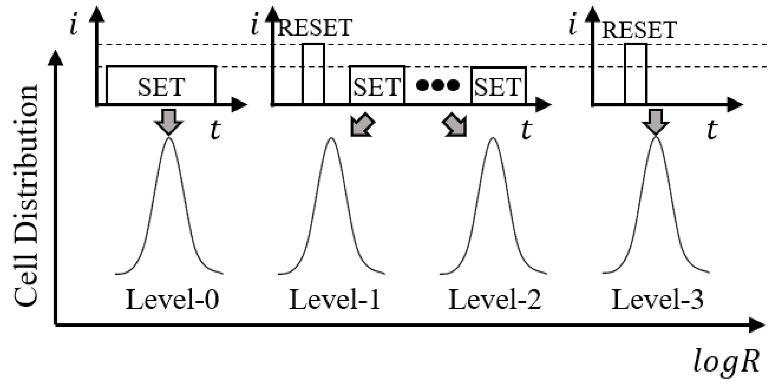
2.1. MLC PCM
2.2. Resistance Drift
2.3. SER Analysis
2.4. PCM-specific Data Encoding Methods
3. Error-vulnerable Pattern-aware Binary-to-Ternary Data Mapping
3.1. LC PCM Characeteristics
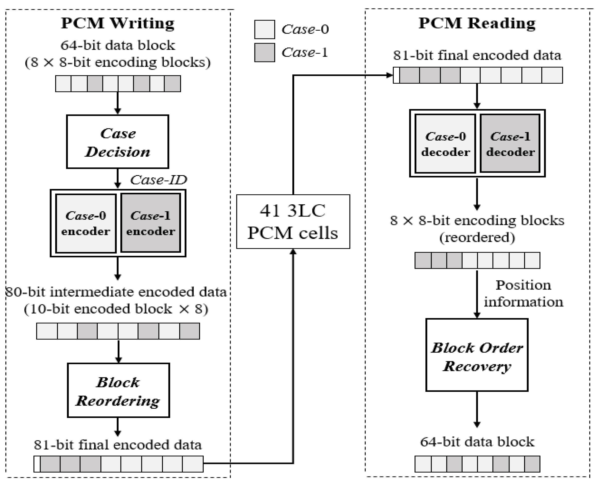
3.2. Overall Two-way Encoding and Decoding Process
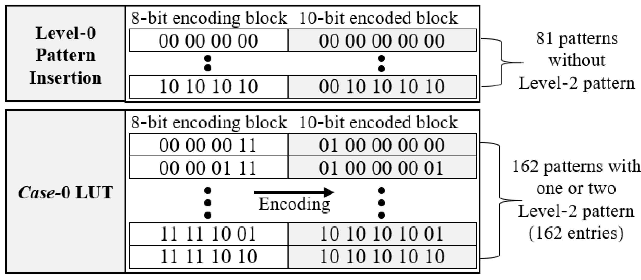
3.3. Two-way Data Encoding Method
3.4. Data Decoding Method
| Algorithm 1 Decoding procedure. | |
| 1: | Input: 81-bit final encoded data |
| 2: | Output: 64-bit data block |
| 3: | |
| 4: | function Decoding |
| 5: | if auxiliary bit == Case-0 // all encoded blocks are Case-0 |
| 6: | perform Case-0 decoder (all encoded blocks) |
| 7: | else |
| 8: | perform Case-0 decoder (all encoded blocks) |
| 9: | perform Case-1 decoder (all encoded blocks) |
| 10: | for i = 1 to 7 do |
| 11: | if Case-ID of next encoded block == Case-0 then |
| 12: | boundary = i + 1 // Set location of Case-0 encoded block cluster |
| 13: | break |
| 14: | end if |
| 15: | end for |
| 16: | |
| 17: | for i = 1 to boundary do |
| 18: | discard datai decoded with Case-0 decoder |
| 19: | place Case-1 encoding block using the 3-bit position information |
| 20: | end for |
| 21: | for i = boundary + 1 to 7 do // if boundary is eight, it means the auxiliary bit is Case-0 |
| 22: | discard datai decoded with Case-1 decoder |
| 23: | place Case-0 encoding block at the remained positions sequentially |
| 24: | end for |
| 25: | end if |
| 26: | end function |
4. Evaluation
4.1. Experimental Setup
4.1.1. Simulation Environment
4.1.2. ECC and Scrubbing Conditions
4.2. Storage Density
4.3. Lifetime
4.4. Performance
5. Conclusions
Author Contributions
Funding
Conflicts of Interest
References
- Lee, B.C.; Zhou, P.; Yang, J.; Zhang, Y.; Zhao, B.; Ipek, E.; Mutlu, O.; Burger, D. Phase-change technology and the future of main memory. IEEE Micro 2010, 30, 131–141. [Google Scholar] [CrossRef]
- Lefurgy, C.; Rajamani, K.; Rawson, F.; Felter, W.; Kistler, M.; Keller, T.W. Energy management for commercial servers. Computer 2003, 36, 39–48. [Google Scholar] [CrossRef]
- Burr, G.; Narayanan, P.; Shelby, R.; Sidler, S.; Boybat, I.; di Nolfo, C.; Leblebici, Y. Large-scale neural networks implemented with non-volatile memory as the synaptic weight element: Comparative performance analysis (accuracy, speed, and power). In Proceedings of the 2015 IEEE International Electron Devices Meeting (IEDM), Washington, DC, USA, 7–9 December 2015. [Google Scholar] [CrossRef]
- Burr, G.W.; Shelby, R.M.; Sidler, S.; Di Nolfo, C.; Jang, J.; Boybat, I.; Shenoy, R.S.; Narayanan, P.; Virwani, K.; Giacometti, E.U. Experimental demonstration and tolerancing of a large-scale neural network (165,000 synapses) using phase-change memory as the synaptic weight element. IEEE Trans. Electron Devices 2015, 62, 3498–3507. [Google Scholar] [CrossRef]
- Jia, G.; Han, G.; Jiang, J.; Liu, L. Dynamic adaptive replacement policy in shared last-level cache of DRAM/PCM hybrid memory for big data storage. IEEE Trans. Ind. Inform. 2016, 13, 1951–1960. [Google Scholar] [CrossRef]
- Tavana, M.K.; Ziabari, A.K.; Kaeli, D. Live together or die alone: Block cooperation to extend lifetime of resistive memories. In Proceedings of the Design, Automation & Test in Europe Conference & Exhibition (DATE), Lausanne, Switzerland, 27–31 March 2017; pp. 1098–1103. [Google Scholar]
- Seong, N.H.; Yeo, S.; Lee, H.-H.S. Tri-level-cell phase change memory: Toward an efficient and reliable memory system. In Proceedings of the 40th Annual International Symposium on Computer Architecture, Tel-Aviv, Israel, 23–27 June 2013; pp. 440–451. [Google Scholar]
- Kwon, T.; Imran, M.; You, J.M.; Yang, J.-S. Heterogeneous PCM array architecture for reliability, performance and lifetime enhancement. In Proceedings of the 2018 Design, Automation & Test in Europe Conference & Exhibition (DATE), Dresden, Germany, 19–23 March 2018; pp. 1610–1615. [Google Scholar]
- Rashidi, S.; Jalili, M.; Sarbazi-Azad, H. Improving MLC PCM performance through relaxed write and read for intermediate resistance levels. ACM Trans. Archit. Code Optim. 2018, 15, 1–31. [Google Scholar] [CrossRef]
- Awasthi, M.; Shevgoor, M.; Sudan, K.; Rajendran, B.; Balasubramonian, R.; Srinivasan, V. Efficient scrub mechanisms for error-prone emerging memories. In Proceedings of the IEEE International Symposium on High-Performance Comp Architecture, New Orleans, LA, USA, 25–29 February 2012; pp. 1–12. [Google Scholar]
- Zhang, W.; Li, T. Helmet: A resistance drift resilient architecture for multi-level cell phase change memory system. In Proceedings of the 2011 IEEE/IFIP 41st International Conference on Dependable Systems & Networks (DSN), Hong Kong, China, 27–30 June 2011; pp. 197–208. [Google Scholar]
- Khouzani, H.A.; Hosseini, F.S.; Yang, C. Segment and conflict aware page allocation and migration in dram-pcm hybrid main memory. IEEE Trans. Comput. Aided Des. Integr. Circuits Syst. 2016, 36, 1458–1470. [Google Scholar] [CrossRef]
- Wang, R.; Zhang, Y.; Yang, J. ReadDuo: Constructing reliable MLC phase change memory through fast and robust readout. In Proceedings of the 2016 46th Annual IEEE/IFIP International Conference on Dependable Systems and Networks (DSN), Toulouse, France, 28 June–1 July 2016; pp. 203–214. [Google Scholar]
- Imran, M.; Kwon, T.; Yang, J.-S. Enrely: A reliable MLC PCM architecture based on data encoding. In Proceedings of the 2019 34th International Technical Conference on Circuits/Systems, Computers and Communications (ITC-CSCC), JeJu, Korea, 23–26 June 2019; pp. 1–4. [Google Scholar]
- Kwon, T.; Imran, M.; Yang, J.-S. Cost-effective reliable MLC PCM architecture using virtual data based error correction. IEEE Access 2020, 8, 44006–44018. [Google Scholar] [CrossRef]
- Thakkar, I.G.; Pasricha, S. DyPhase: A dynamic phase change memory architecture with symmetric write latency and restorable endurance. IEEE Trans. Comput.-Aided Des. Integr. Circuits Syst. 2017, 37, 1760–1773. [Google Scholar] [CrossRef]
- Das, A.; Sánchez-Macián, A.; García-Herrero, F.; Touba, N.A.; Maestro, J.A. Enhanced limited magnitude error correcting codes for multilevel cell main memories. IEEE Trans. Nanotechnol. 2019, 18, 1023–1026. [Google Scholar] [CrossRef]
- Gang, W. Threat models and security of phase-change memory. In Proceedings of the 2019 IEEE International Conference on Consumer Electronics (ICCE), Las Vegas, NV, USA, 11–13 January 2019; pp. 1–6. [Google Scholar]
- Mittal, S. A survey of soft-error mitigation techniques for non-volatile memories. Computers 2017, 6, 8. [Google Scholar] [CrossRef]
- Zhao, M.; Xue, Y.; Hu, J.; Yang, C.; Liu, T.; Jia, Z.; Xue, C.J. State asymmetry driven state remapping in phase change memory. IEEE Trans. Comput.-Aided Des. Integr. Circuits Syst. 2016, 36, 27–40. [Google Scholar] [CrossRef]
- Yoon, D.H.; Chang, J.; Schreiber, R.S.; Jouppi, N.P. Practical nonvolatile multilevel-cell phase change memory. In Proceedings of the SC’13: Proceedings of the International Conference on High Performance Computing, Networking, Storage and Analysis, Denver, CO, USA, 17–22 November 2013; pp. 1–12. [Google Scholar]
- El-Hassan, N.H.; Kumar, T.N.; Almurib, H.A.F. Implementation of time-aware sensing technique for multilevel phase change memory cell. Microelectron. J. 2016, 56, 74–80. [Google Scholar] [CrossRef]
- Kim, N.S.; Song, C.; Cho, W.Y.; Huang, J.; Jung, M. LL-PCM: Low-latency phase change memory architecture. In Proceedings of the 56th Annual Design Automation Conference 2019, Las Vegas, NV, USA, 2–6 June 2019; pp. 1–6. [Google Scholar]
- Lue, H.-T.; Hsu, T.-H.; Wang, S.-Y.; Lai, E.-K.; Hsieh, K.-Y.; Liu, R.; Lu, C.-Y. Study of incremental step pulse programming (ISPP) and STI edge effect of BE-SONOS NAND flash. In Proceedings of the 2008 IEEE International Reliability Physics Symposium, Phoenix, AZ, USA, 27 April–1 May 2008; pp. 693–694. [Google Scholar]
- Ielmini, D.; Boniardi, M.; Lacaita, A.L.; Redaelli, A.; Pirovano, A. Unified mechanisms for structural relaxation and crystallization in phase-change memory devices. Microelectron. Eng. 2009, 86, 1942–1945. [Google Scholar] [CrossRef]
- Kim, S.; Lee, B.; Asheghi, M.; Hurkx, F.; Reifenberg, J.P.; Goodson, K.E.; Wong, H.-S.P. Resistance and threshold switching voltage drift behavior in phase-change memory and their temperature dependence at microsecond time scales studied using a micro-thermal stage. IEEE Trans. Electron Devices 2011, 58, 584–592. [Google Scholar] [CrossRef]
- Sebastian, A.; Papandreou, N.; Pantazi, A.; Pozidis, H.; Eleftheriou, E. Non-resistance-based cell-state metric for phase-change memory. J. Appl. Phys. 2011, 110, 084505. [Google Scholar] [CrossRef]
- Yu, S.; Chen, P.-Y. Emerging memory technologies: Recent trends and prospects. IEEE Solid-State Circuits Mag. 2016, 8, 43–56. [Google Scholar] [CrossRef]
- Schroeder, B.; Pinheiro, E.; Weber, W.-D. DRAM errors in the wild: A large-scale field study. ACM SIGMETRICS Perform. Eval. Rev. 2009, 37, 193–204. [Google Scholar] [CrossRef]
- Binkert, N.; Beckmann, B.; Black, G.; Reinhardt, S.K.; Saidi, A.; Basu, A.; Hestness, J.; Hower, D.R.; Krishna, T.; Sardashti, S. The gem5 simulator. ACM SIGARCH Comput. Archit. News 2011, 39, 1–7. [Google Scholar] [CrossRef]
- Poremba, M.; Zhang, T.; Xie, Y. Nvmain 2.0: A user-friendly memory simulator to model (non-) volatile memory systems. IEEE Comput. Archit. Lett. 2015, 14, 140–143. [Google Scholar] [CrossRef]
- Henning, J.L. SPEC CPU2006 benchmark descriptions. ACM SIGARCH Comput. Archit. News 2006, 34, 1–17. [Google Scholar] [CrossRef]
- Nair, A.A.; John, L.K. Simulation points for SPEC CPU 2006. In Proceedings of the 2008 IEEE International Conference on Computer Design, Lake Tahoe, CA, USA, 12–15 October 2008; pp. 397–403. [Google Scholar]
- Joshi, M.; Zhang, W.; Li, T. Mercury: A fast and energy-efficient multi-level cell based phase change memory system. In Proceedings of the 2011 IEEE 17th International Symposium on High Performance Computer Architecture, San Antonio, TX, USA, 12–16 February 2011; pp. 345–356. [Google Scholar]
- Dong, X.; Xu, C.; Xie, Y.; Jouppi, N.P. Nvsim: A circuit-level performance, energy, and area model for emerging nonvolatile memory. IEEE Trans. Comput.-Aided Des. Integr. Circuits Syst. 2012, 31, 994–1007. [Google Scholar] [CrossRef]
- Strukov, D. The area and latency tradeoffs of binary bit-parallel BCH decoders for prospective nanoelectronic memories. In Proceedings of the 2006 Fortieth Asilomar Conference on Signals, Systems and Computers, Pacific Grove, CA, USA, 29 October–1 November 2006; pp. 1183–1187. [Google Scholar]


| Level | Pattern | ||||
|---|---|---|---|---|---|
| 0 | 00 | 3 | 0.01 | 0.004 | |
| 1 | 01 | 4 | 0.02 | 0.008 | |
| 2 | 11 | 5 | 0.06 | 0.024 | |
| 3 | 10 | 6 | 0.1 | 0.04 | |
| Scrubbing Period (s) | No ECC | BCH-8 (80 Parity Bits) | BCH-16 (160 Parity Bits) | BCH-24 (240 Parity Bits) |
|---|---|---|---|---|
| Negligible | Negligible | |||
| Negligible | Negligible | |||
| Negligible | Negligible | |||
| Negligible | ||||
| Negligible | ||||
| 3-Digit Binary Values | 2-Digit Ternary Values |
|---|---|
| 000 | 00 |
| 001 | 01 |
| 010 | 12 |
| 011 | 02 |
| 100 | 10 |
| 101 | 20 |
| 110 | 22 |
| 111 | 21 |
| Case-ID | # of Level-2 Patterns | Example | # of Possible Patterns |
|---|---|---|---|
| Case-0 | 0 | 00 00 00 00 | 81 |
| 1 | 11 00 01 10 | 108 | |
| 2 | 11 11 00 01 | 54 | |
| Case-1 | 3 | 11 11 11 00 | 12 |
| 4 | 11 11 11 11 | 1 |
| Cores | 4-Core, Alpha, 2 GHz |
| L1 I/D Cache | 32 KB, 2-way, 2-cycle latency |
| L2 Cache | 1 MB, 8-way, 20-cycle latency |
| L3 Cache | 16 MB, 16-way, 50-cycle latency |
| Main Memory | MLC PCM, 16 GB, 400 MHz clock |
| Number of banks | 8 (2 GB for each bank) |
| Memory Controller | FRFCFS |
| Memory write latency (pattern) [34] | 150 ns (00), 200 ns (01), 210 ns (11), 60 ns (10) |
| Scrubbing Period (s) | 4LC PCM | HPCM [8] | RWR [9] | CRPCM [15] | 3LC PCM [7] | Proposed |
|---|---|---|---|---|---|---|
| BCH-16 | BCH-12 | BCH-12 | BCH-16 | No ECC | No ECC | |
| Negligible | Negligible | Negligible | Negligible | Negligible | Negligible | |
| Negligible | Negligible | Negligible | Negligible | Negligible | Negligible | |
| Negligible | Negligible | Negligible | Negligible | Negligible | Negligible | |
| Negligible | Negligible | Negligible | Negligible | |||
| Negligible | Negligible | |||||
| Negligible | Negligible | |||||
| Negligible | Negligible |
| Related Studies | Number of PCM Cells (for 512-Bit Cache Line) | Storage Density | |||
|---|---|---|---|---|---|
| Data Cells | Parity Cells | Add. Cells | Total Cells | ||
| 4LC PCM (BCH-16) | 256 | 80 | 0 | 336 | 152.4% |
| RWR (BCH-12) [9] | 256 | 60 | 32 | 338 | 151.5% |
| HPCM (BCH-12) [8] | 384 | 43 | 0 | 427 | 119.9% |
| CRPCM (BCH-16) [15] | 256 | 73 | 0 | 329 | 155.6% |
| 3LC PCM [7] | 384 | 0 | 0 | 384 | 133.3% |
| Proposed | 320 | 0 | 4 | 324 | 157.1% |
| Module | Area Per Bank (mm2) |
|---|---|
| Memory cells | 2.466 |
| Peripheral circuits | 0.326 |
| Proposed encoder | 0.007 |
| Proposed decoder | 0.008 |
| Area overhead | 0.52% |
© 2020 by the authors. Licensee MDPI, Basel, Switzerland. This article is an open access article distributed under the terms and conditions of the Creative Commons Attribution (CC BY) license (http://creativecommons.org/licenses/by/4.0/).
Share and Cite
Hong, J.B.; Lee, Y.S.; Kim, Y.W.; Han, T.H. Error-Vulnerable Pattern-Aware Binary-to-Ternary Data Mapping for Improving Storage Density of 3LC Phase Change Memory. Electronics 2020, 9, 626. https://doi.org/10.3390/electronics9040626
Hong JB, Lee YS, Kim YW, Han TH. Error-Vulnerable Pattern-Aware Binary-to-Ternary Data Mapping for Improving Storage Density of 3LC Phase Change Memory. Electronics. 2020; 9(4):626. https://doi.org/10.3390/electronics9040626
Chicago/Turabian StyleHong, Jeong Beom, Young Sik Lee, Yong Wook Kim, and Tae Hee Han. 2020. "Error-Vulnerable Pattern-Aware Binary-to-Ternary Data Mapping for Improving Storage Density of 3LC Phase Change Memory" Electronics 9, no. 4: 626. https://doi.org/10.3390/electronics9040626
APA StyleHong, J. B., Lee, Y. S., Kim, Y. W., & Han, T. H. (2020). Error-Vulnerable Pattern-Aware Binary-to-Ternary Data Mapping for Improving Storage Density of 3LC Phase Change Memory. Electronics, 9(4), 626. https://doi.org/10.3390/electronics9040626


