1. Introduction
More electric aircraft (MEA) and all electric aircraft (AEA) are concepts which can only be effective if power converters have a significant reduction in losses and weight. This is now enabled by the use of disruptive technology such as SiC and GaN semiconductors. This technology helps to increase switching frequency and, thus, to reduce filtering needs and/or to reduce semiconductor losses. This loss reduction may eliminate the use of liquid cooling inside aircrafts, with a consequent improvement in reliability and reduction in maintenance cost.
Electrical network in future aircrafts will have higher voltage than actual aircrafts in order to reduce conductor weight. There is a consensus on having 540 V in direct current (DC) buses of Airbus aircrafts. For the voltage level, 1200-V SiC components are the best candidates for boosting efficiency [
1,
2] and power density [
3] of new power converters. Nevertheless, there is a lack of information on datasheets about losses and reliability, and the design of a converter cannot be precisely made with this information.
Semiconductor losses depend on conduction losses and switching losses in a power converter. Conduction losses can be precisely calculated using datasheet values. However, switching losses in datasheets of SiC and GaN components are, most of the time, either inexistent or inaccurate [
4]. The authors in References [
5,
6] performed precise loss calculations in power converters based on the double pulse method (DPM) and the modified opposition method (MOM), respectively, to measure switching energy. Since the MOM method gives more precise results, especially for very fast components such as SiC and GaN, this method is used in the work presented here.
Therefore, this paper aims to recall and give more details to explain the approach to precisely calculate losses in three-phase inverters using experimental data from an accurate characterization of switching energies of wide bandgap (WBG) components. This approach was first presented in Reference [
6], and it allows us to show the influence of different pulse width modulation (PWM) methods on losses of a three-phase inverter with floating neutral point.
PWM methods are used to optimize certain characteristics of the power converter. Some of them were created in the 1970s and 1980s to reduce losses in three-phase inverters [
7]. They are based on preventing switching when the converter current is high, in each phase. Optimal PWM methods can be created, as shown in Reference [
8], even for SiC-based power converters. However, the aim here is, unlike other papers, not to reduce losses, but to show the influence of PWM methods and other converter parameters on SiC-based converter losses, specifically on the temperature variation in SiC dies, which is directly related to the power module reliability.
Although WBG components such as silicon carbide (SiC) or gallium nitride (GaN) transistors have higher performance than their silicon (Si) counterparts, their reliability data are either reduced or non-existent. Some works showed reduced reliability on SiC dies, when compared to Si-based switches, due to degradation of the oxide–semiconductor interface [
9] or the body diode characteristics [
10]. The lack of reliability data and the general feeling in the community about the low reliability of these components are hindering their use and consequently holding back the performance of static converters.
Another significant source of failure in a static converter is the power modules. In a single die, the reliability of a power module depends on its average temperature, which can be higher in SiC-based power modules when compared to their Si-based counterparts. High average temperature may significantly reduce the reliability of power modules [
11,
12]. However, reliability strongly depends on thermal cycles mainly caused by these components [
13,
14]. Thermal cycles are the main source of failure in power modules, especially due to the effect of breaking the connections between the dies and bond wires, due to the mechanical fatigue caused by dilations and contractions resulting from these thermal cycles [
14]. This issue is even more important in SiC-based modules since SiC dies are smaller (for the same rated current and voltage) and, as a consequence, have lower thermal capacitance and higher amplitude of thermal cycles, which reduce reliability [
15]. One of the main problems to investigate is, therefore, finding how to increase the reliability of converters based on SiC power modules, for example, by controlling thermal cycles of these components.
The work presented here also evaluates the various parameters of a three-phase inverter having an influence on the thermal cycles of a SiC power module. Specifically, we focus on reducing the amplitude of these thermal cycles at the fundamental frequency of the current flowing through the power module via the use of different PWM modulation methods applied to the converter.
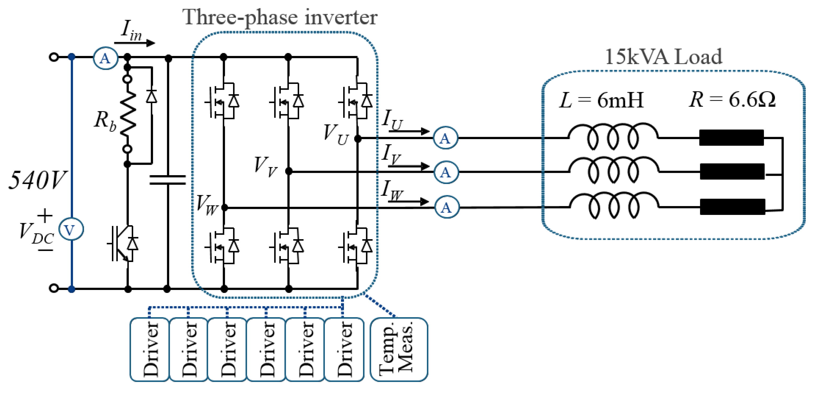
As a test platform to verify the method presented here, a three-phase SiC inverter, represented in
Figure 1, was designed using a 1200-V/50-A six-pack SiC module from WOLFSPEED (reference CCS050M12CM2) to be connected in the DC bus of 540 V and in a 15-kVA load. This converter was built as flexible as possible so that different parameters could be changed in order to verify their influence on losses and junction temperature variation. These parameters were as follows: driver parameters (gate resistance and voltage), converter parameters (input voltage, output current, output current ripple), and controller parameters (dead time, switching frequency, PWM method).
Experimental results were obtained using the designed three-phase SiC converter and they verified the approach developed to precisely calculate the losses and thermal cycles of SiC inverters. Moreover, these results confirmed loss and temperature amplitude reduction in the converter when using different PWM methods.
The problem of reducing the reliability of converters and the lifetime of power modules due to thermal cycling is discussed in
Section 2.
Then, in
Section 3, the precise calculation of switching and conduction losses in SiC components is presented. These calculations are very important to estimate the junction temperature swing of SiC dies inside a power module.
Section 4 shows the influence of different PWM methods and other parameters on the instantaneous losses observed in semiconductors.
The switching energy measurement and loss calculation procedure are validated using the experimental results of losses in a three-phase SiC inverter for different PWM methods, which are presented in
Section 5.
In
Section 6, the calculated losses are used to estimate the temperature variation of SiC dies according to several parameters, as well as PWM methods, which allow us to choose those that increase the reliability of the converter.
2. Thermal Stress and Reliability of SiC Modules
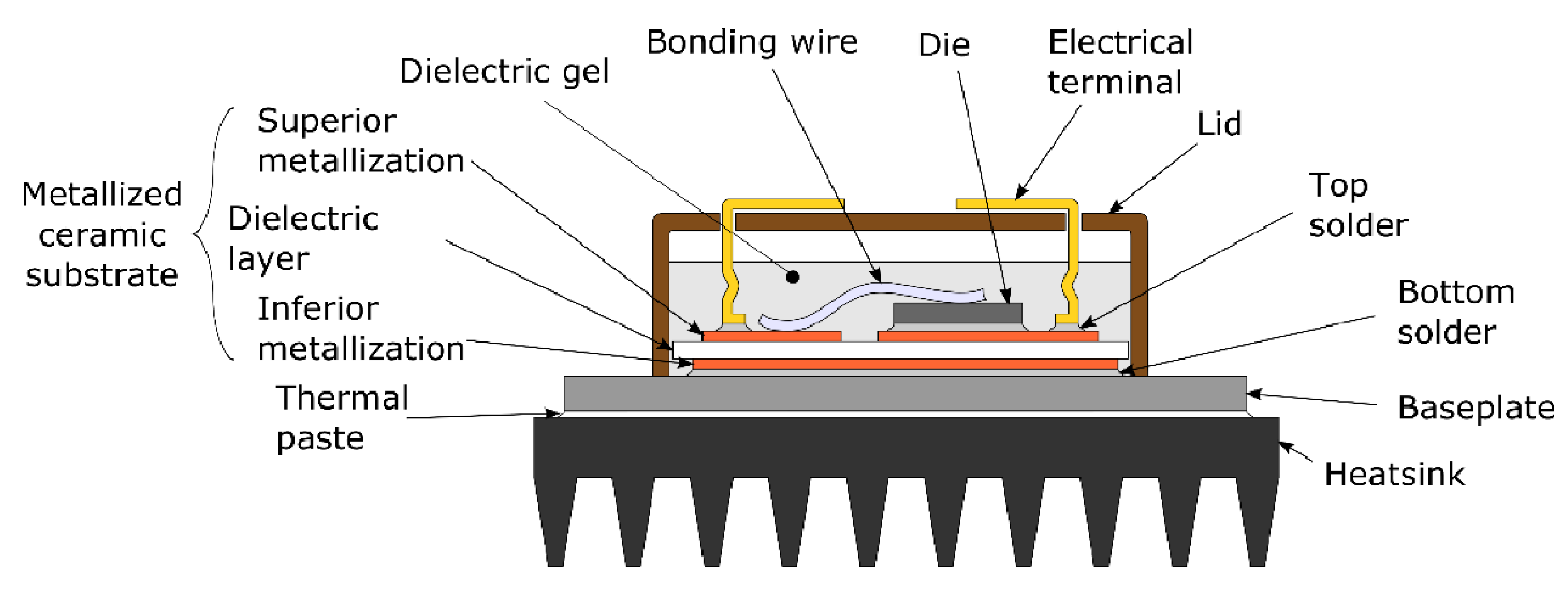
In a power module composed of IGBT or MOSFET dies, the most fragile connection and, therefore, that having the lowest reliability, constitutes the bond wires, as shown in
Figure 2 (extracted from Reference [
16]). This fragile connection is located between the upper metallization of the substrate and the upper metallization of the die. The temperature variation of the die causes dilations and contractions of its structure, which leads to its fatigue and eventually to a wire bond crack close to the die metallization, which reduces the module lifetime.
Several studies [
11,
17] carried out on commercial IGBTs and MOSFETs showed how the number of thermal cycles leading to the failure of a power module varies with the amplitude of these thermal cycles and the average temperature of the module. As an example,
Figure 3, taken from Reference [
17], shows this variation for a power module using power MOSFET for automotive applications. Notice in this figure that thermal cycles with an amplitude of 40 °C lead to a number close to 12 × 10
6 cycles until module failure. In the case where the amplitude of the thermal cycles (Δ
T) is reduced to 20 °C, for example, the number of cycles to failure would rise to about 50 × 10
6. By applying a logarithmic extrapolation of the curve shown in
Figure 3, we may expect that the number of cycles until module failure is 90 × 10
6 if the amplitude of thermal cycles is reduced to 10 °C.
Note that the number of cycles at ΔT = 10 °C is very high. Nevertheless, the lifetime of this power module can be low, even at this level of ΔT, if the number of cycles per unit of time is high. This is the case for thermal cycling of dies due to sinusoidal current flowing through these components, in applications such as inverters for motor control or inverters used to create grid voltage (230 V/50 Hz) in future aircrafts.
The amplitude of thermal cycles at the fundamental frequency of current (and, therefore, the instantaneous power) flowing through the die depends on the thermal capacitance of the die, as well as that of the power module where the die is integrated. In a power converter, even if the power module is attached to a heat sink with very high heat capacity, the semiconductor die presents thermal cycles at the fundamental frequency of current, and this creates die dilations and contractions which may cause reduction of power module lifetime.
Since the SiC dies are smaller than those based on Si, for the same current rating, the thermal capacitance of SiC-based power modules is lower than that of the Si-based modules. As a consequence, the amplitude of thermal cycles in SiC dies inside modules is higher than that in Si dies in modules and, consequently, they may present shorter lifetime.
In order to increase lifetime of a power module, the number and amplitude of thermal cycles should be reduced. This amplitude can be reduced by decreasing the amplitude of instantaneous power dissipated by the dies, which can be done by using different PWM methods or dynamically changing some other parameters which have an influence on losses, as shown in
Section 4. However, in order to reduce these thermal cycle amplitudes, it is necessary to estimate the junction temperature (
Tj) of the dies at each instant by using not only the thermal impedance given by the manufacturers (or estimated by characterization), but also the precise loss estimation in each die.
Loss estimation involves the accurate calculation of conduction and switching losses for each switched current. For this, one needs precise models, which are shown below.
3. Precise Loss Calculation in Three-Phase Converters
Most of the losses in a three-phase inverter are due to the losses in power transistors. These losses depend on conduction and switching losses. Both types of losses depend on the current waveform flowing in each phase.
3.1. Conduction Losses
Conduction losses are relatively simple to precisely calculate. The current in each phase, which mainly depends on the imposed output voltage and the load impedance, flows through both components in a switching leg, one at a time. Total conduction losses in this switching leg can be simply calculated as
where
IoRMS is the RMS value of this current (composed of fundamental value and harmonics) and
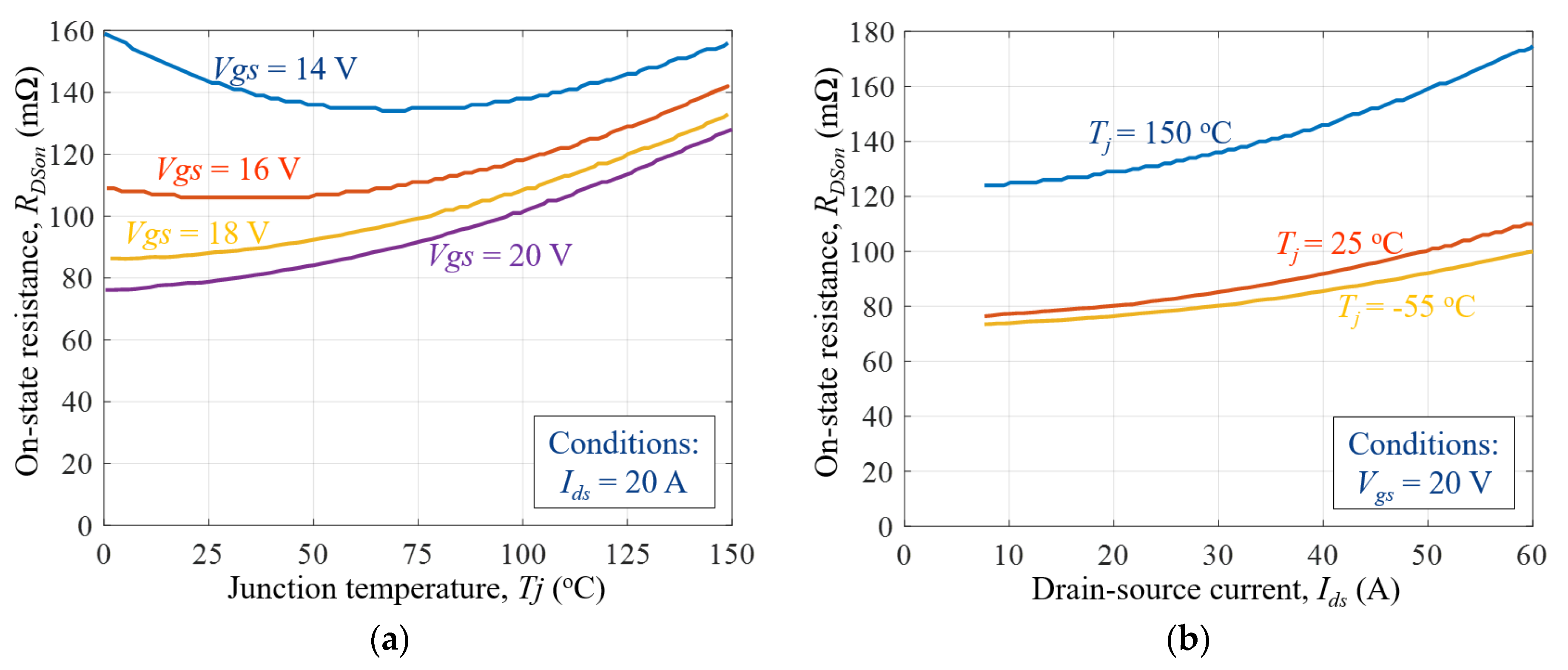
RDSon is the on-state resistance of a MOSFET at a certain junction temperature, for a given junction temperature. For the SiC power module used in this work (CCS050M12CM2 from Wolfspeed),
RDSon at 25 °C was 25 mΩ and it increased with the temperature. At the maximum junction temperature, 150 °C, this resistance increased to 43 mΩ.
If we consider a symmetrical and balanced system, half the losses are dissipated in the high-side transistor and the other half are dissipated in the low-side transistor. However, in order to calculate temperature variation, as shown in
Section 6, instantaneous losses must be precisely calculated in each transistor, as well as the diode, in the case where power modules have diodes in parallel to transistors.
Independently, if the power module has only SiC MOSFETs inside, or diode components in parallel to the body diode of SiC MOSFETs, the current flows through these diodes during the dead time. Thus, during dead time, these diodes present conduction losses, which are considered as switching losses, since they exist only when there is a commutation in a switching leg. These losses are explained in the next subsection.
However, external diodes can also present conduction losses when the switch is operating in the third quadrant. In this state, current is shared between the SiC MOSFET channel and the diode. However, when using power modules in very-high-efficiency (>99%) converters, current flowing through the switch is relatively low. Low current in an association of SiC MOSFET and diode only flows through the SiC MOSFET channel. As an example, component CCS050M12CM2 from Wolfspeed, used in this work, has a third quadrant curve showing that, at 25 °C, current starts flowing through the diode when the switch current is higher than 37 A. In the 15-kVA application of this work, the maximum peak current in each phase of the three-phase inverter is around 40 A. For this reason, we consider in the explanations below that the diode components inside the SiC power module do not present conduction losses. This is obviously not the case for lower-efficiency applications.
Instantaneous conduction losses of each transistor
Pcond(
t) are calculated using instantaneous values of current flowing through the component
Ids(
t), as well as the on-state resistance
RDSon of this transistor at this specific time, which depends on the junction temperature
Tj, gate-source voltage
Vgs, and the current flowing through the component, as can be seen in the graphs extracted from the component datasheet, shown in
Figure 4. These losses can be calculated as
An algorithm using MATLAB was created to compute conduction losses in the two transistors of one leg of a three-phase inverter using the reference SiC module of this work. As an example, we show results for driver parameters (gate-source voltage Vgs = −4V/20 V, gate resistance Rg = 10 Ω, and dead time DT = 400 ns) and system parameters (DC bus voltage VDC = 540 V, output current Iout = 26.3 A, angle between fundamental values of output current and voltage φ = 0°, modulation index Mi = 1, and switching frequency Fsw = 50 kHz). At this operation point, output power was Pout = 15kW, sinusoidal modulation was used, and the current ripple was considered to be negligible. These values were calculated for a junction temperature of components Tj = 55 °C.
Conduction losses at each instant were calculated numerically for each point of the output current in a period of the fundamental frequency of the output current
Io. This current was multiplied by the switching signal (
S) of the considered transistor to find the instantaneous current in the transistor.
In order to calculate the instantaneous conduction losses, as in Equation (2), for each calculation point, one must firstly find the value of
RDSon. Since
Vgs is usually fixed when the transistor is on, and since the junction temperature does not significantly vary during a fundamental period (as shown in
Section 6),
RDSon must be calculated for each current
Ids. For that, we used curves of
Figure 4b at
Tj = 25 °C and the one
Tj = 150 °C, and we applied a linear interpolation to find
RDSon for a given current
Ids, as shown below.
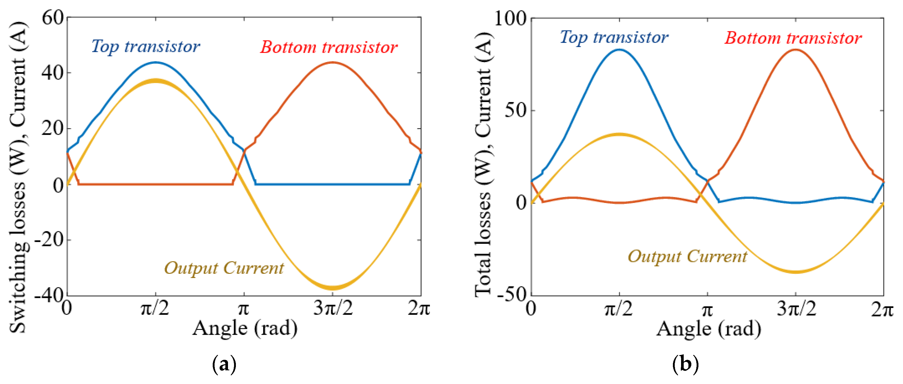
Calculated instantaneous losses, for the parameters shown above, in each transistor are shown in
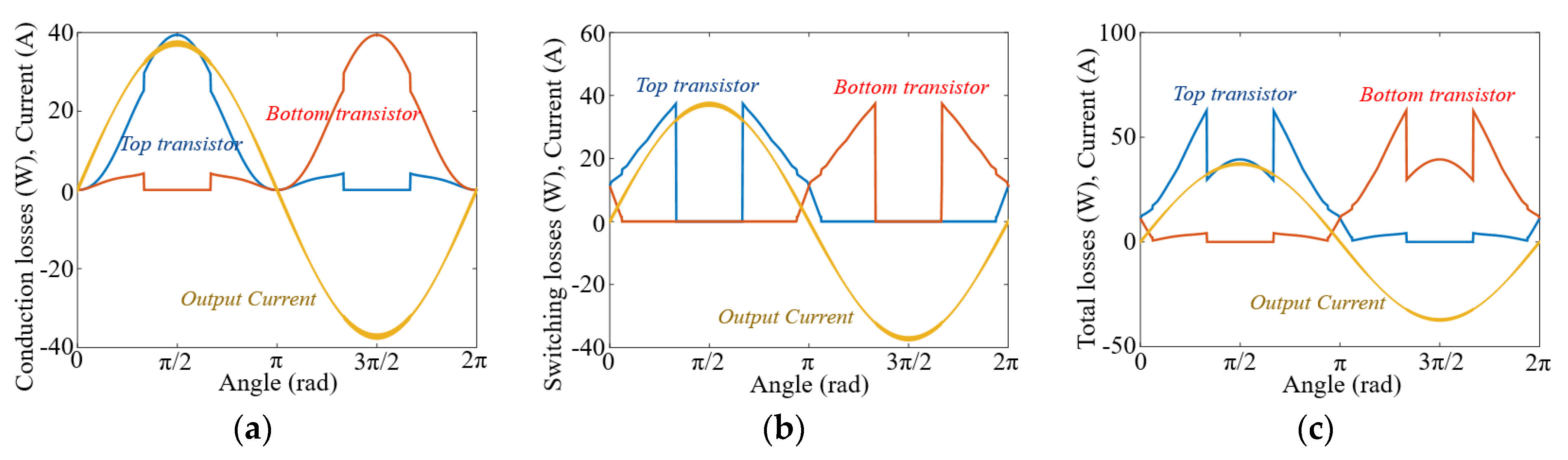
Figure 5a, as well as the output current. Since switching frequency is much higher than the fundamental, it is difficult to identify the duty cycle and estimate average losses by these waveforms. A more intuitive way to show these losses is by taking the average in a switching period. By doing that, conduction losses in each transistor, averaged over a switching period, are shown in
Figure 5b, together with the output current. Note that, when the current was positive, most of the conduction losses was dissipated in the high-side transistor. On the contrary, when current was negative, most of the losses were observed at the low-side transistor. This conclusion obviously depends on the angle between the output current and voltage (i.e., the power factor).
3.2. Switching Losses
Switching losses are significantly more complicated to estimate, since there is not enough data given by manufacturers or they may not be representative of switching losses in the real converter.
Switching energies in datasheets are often measured using the “double pulse” method [
18]. This method has serious drawbacks, as pointed out in Reference [
4], mainly because the current in the component must be measured. A more accurate method for measuring switching losses in fast components such as SiC and GaN transistors is called the “modified opposition method”, which is explained in Reference [
4]. This method consists of an association of two identical half bridges containing the four identical devices (SiC MOSFETs in this case) supplied by the same source and connected through an inductor. Turn-on and turn-off energies are estimated by the total losses measured in the system, with no need to measure current in any transistor.
This method was applied to characterize the CCS050M12CM2 SiC module from WOLFSPEED, which was the six-pack 1200-V/50-A SiC module of reference in this work, and which was used in the developed three-phase inverter.
Figure 6 presents the switching energies measured with the method explained above for different currents, for two different DC bus voltages (270 and 540 V) and for the following parameters: gate resistance
Rg = 10 Ω, gate-source voltage
Vgs = −4 V/20 V, and dead time
DT = 400 ns. These values were obtained at room temperature
T = 25 °C.
The switching energy during turn-on and turn-off measured in this component includes not only the energy lost during commutation but also the energy lost in the diode of the opposite switch during dead time. At a dead time of 400 ns, as in the example of
Figure 6, losses in the diode correspond to a maximum of 4.5% of total switching energy in the worst case when current is the highest (40 A peak in the output of the 15-kVA converter). For that reason, for the sake of simplification, we decided to include these losses in the transistor which was switching although they happened in the opposite diode (either the body diode of the opposite SiC MOSFET or a diode component anti-parallel to the SiC MOSFET, which was the case in the reference SiC Module, CCS050M12CM2). Note that, by doing this approximation, total switching losses were precisely calculated, but the instantaneous switching losses in the transistor were slightly overestimated, which did not change the analysis in
Section 6.
Using the waveform of the output current, for each duty cycle of a fundamental period, the switched current can be determined. Then, depending on the current sign and output voltage commutation (from −
VDC/2 to +
VDC/2 or vice versa), we can determine if a turn-off or turn-on energy was lost. Using this information and the curve shown in
Figure 6, the switching energy at each switching period can be calculated for the whole fundamental period and switching losses can be estimated. Note that different switching ripples can significantly change switching losses, as shown in Reference [
19].
Using the same MATLAB algorithm and parameters cited above, switching losses in the components of one leg of the three-phase inverter using the SiC module were calculated. The total switching energy lost in a switching period divided by the switching period value gave an idea of the switching losses in each switching period. For the example above, these instantaneous switching losses averaged in a switching period are shown in
Figure 7a, as well as the output current. Total losses (conduction and switching) in each transistor are shown in
Figure 7b. Note that the highest conduction and switching loss values occurred at the highest output current. Thus, in order to reduce losses and consequently increase efficiency of the inverter, instead of using a simple sinusoidal PWM method, other methods can be used to reduce losses, for example, specifically at the moments where they are at their maximum. This is explained below.
4. Loss Variation for Different Parameters
4.1. Influence of PWM Methods on Converter Losses
As shown above, switching losses depend not only on the switching frequency but also on the current which is being switched. Different PWM methods may change the effective switching frequency, as well as the converter current, consequently altering semiconductor losses.
There are different PWM methods. Some of them consist of modifying the voltage reference of each phase by adding offsets to the reference of each phase. This common-mode voltage applied to the three phases is found in the neutral point of the load (which is floating) and, as a result, the phase-neutral voltage in each phase of the load has exactly the waveform of the original reference (usually a sinusoidal waveform). This degree of freedom (common-mode voltage in all three phases) was initially used in inverters in order to increase the linearity range of the output voltage and later to reduce the THD of the output current or to reduce switching losses in the converter.
PWM methods are usually identified as continuous PWM (CPWM) and discontinuous PWM (DPWM) methods. CPWM modulation waveforms are always strictly within the boundaries imposed by the triangular carriers while DPWM references can vary outside carrier bands, resulting in output voltage clamped to the positive and/or negative DC rail. If no low-frequency distortion of the output voltage is allowed, clamping may be imposed at most 120° of the reference wave in each phase. This clamping results in no commutation in one of the phases for at most one-third of the fundamental period. As a result, switching losses are reduced, as well as total losses.
Many PWM methods can be found in Reference [
7]. Those considered for comparison in this work are the following: SPWM, THIPWM, SVPWM, DPWMMIN, DPWMMAX, DPWM0, DPWM1, DPWM2, DPWM3, and PWMBC [
20].
One of these methods is DPWM1, which clamps the reference into the positive rail for 60° centered at the maximum value of the sinusoidal reference, and which also clamps the reference into the negative rail for 60° centered at the minimum value of the sinusoidal reference. The result of this method in conduction, switching, and total losses of semiconductor for the same conditions of the example above (
Figure 6 and
Figure 7) is shown in
Figure 8. Note that, in each transistor, there are no switching losses and no conduction losses at 60°. Additionally, as in any inverter, there are also no switching losses at almost half cycle depending on the output current sign. Total losses in the three phases of the power module decrease from around 152 W to 110 W when changing the PWM method from SPWM to DPWM1. Confirmation of the loss calculation procedure shown here and the loss variation for different PWM methods are shown using the experimental set-up below.
4.2. Impact of Other Parameters on Semiconductor Losses
The PWM method may change losses in different ways depending on the parameters that can be changed in a three-phase inverter, such as the value and the frequency of the fundamental current, the gate resistance and gate-source voltage applied to the SiC module, the modulation index
Mi, the angle between the current and the voltage
φ, and the switching frequency
Fsw.
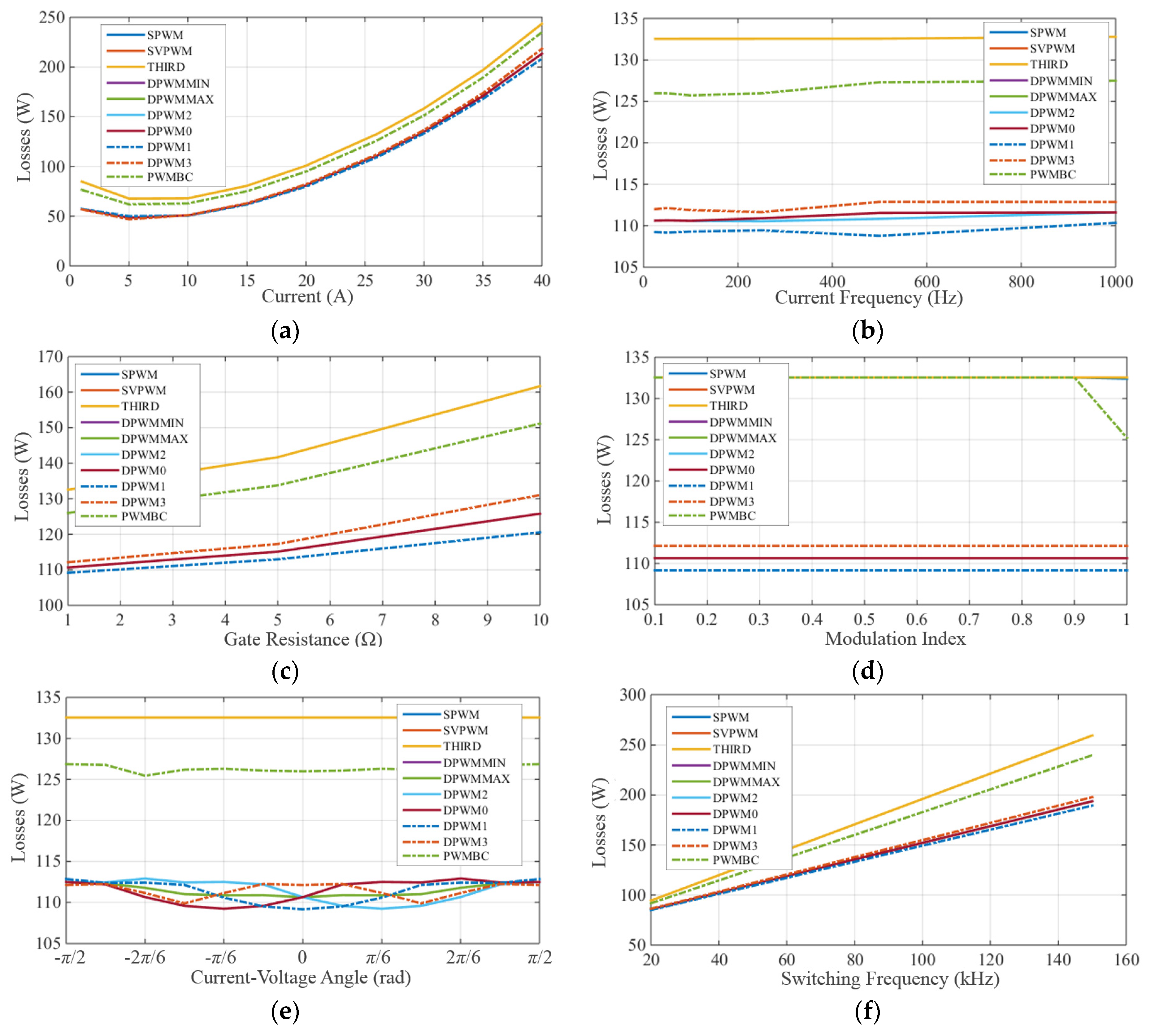
Figure 9 shows the calculated total semiconductor losses for each PWM method, as well as for the variation of each parameter cited above. The fixed parameters are the same as those shown in
Section 3.
Note that losses may change with the PWM method. Continuous PWM methods, such as SPWM, SVPWM, and THIPWM, present the same losses since there is no variation in the switched current and the effective switching frequency remains the same. However, for discontinuous PWM methods, losses are different because each method imposes no commutation at different angles of the fundamental current.
Concerning the other parameters, losses greatly increase with the current value, switching frequency, and gate resistance. However, almost no loss variation is observed when changing the output current frequency, the angle between this current and the output voltage, and the modulation index. This conclusion is not same when analyzing the junction temperature swing for these different parameters, as shown in
Section 6. The next section experimentally validates the losses calculated in this work.
5. Validation of Loss Calculation by Experimental Results
In order to verify the loss calculated in a three-phase inverter, this converter was designed and fabricated using the reference SiC power module (CCS050M12CM2 from Wolfspeed), as shown in
Figure 10.
Figure 11 shows the experimental set-up to test the converter and evaluate its efficiency. Power measurements in the input and output of each phase were performed using a ZES ZIMMER LMG640 high-bandwidth high-precision power analyzer. A passive three-phase RL load of 6.6 Ω and 6 mH per phase was connected to the output of the inverter as shown in
Figure 1. This load had an angle of
ϕ = 17° at a fundamental frequency of 50 Hz. Generic flexible drivers were designed to drive the SiC module. The fixed parameters for the experimental results shown here were gate-to-source voltage
Vgs = −4 V/20 V and gate resistance
Rg = 10 Ω.
Losses on the three-phase inverter were measured for different PWM methods and for the parameters shown above. Since the system was running on an open loop, the output current and power varied for different PWM methods, but all the output currents were between 23.6 and 25.2 A (output power from 12 to 13.5 kVA). Measured losses are shown in
Table 1. In this table, we also show the corresponding losses calculated using the MATLAB algorithm developed and described above. We added the calculation of some fixed losses existing in the real three-phase inverter such as losses on connections (around 10 mΩ of connection resistance on input and an average of 5.7 mΩ of connection resistance in each output), as well as on resistances to discharge the bus capacitors (2.2 W). All these “extra” resistances were measured separately. Furthermore, the resistance of each transistor inside the SiC module was measured (average of 25.25 mΩ for the six transistors at 25 °C) and the temperature of the SiC module case was measured to accurately estimate conduction losses.
Estimated inverter losses were about 6% lower than those of experimental measurements. This difference can be explained by non-modeled losses such as connection losses at high frequency (switched current between switches and bus capacitors), as well as the loss measurement precision given the poor accuracy of the power analyzer in this configuration (only about 1% of the total measured power in the input and the output represents the losses). Accurate power measurements at such high efficiency are an important challenge as shown in Reference [
21]. Moreover, the accuracy of the measured losses is reduced by the high-frequency voltage in the output of the converter (
Fsw = 50 kHz).
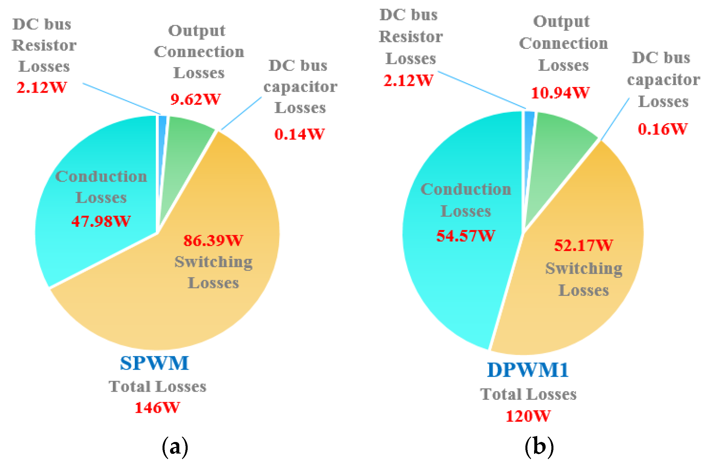
At such a high frequency, switching losses constitute an important part of total losses, as can be seen in
Figure 12, where we show the total estimated losses for two different PWM methods using the measured currents at maximum output power. Note that switching losses account for about 60% and 43% of total losses for SPWM and DPWM1 methods, respectively. This confirms that switching losses were precisely calculated using the switching measurement method shown above.
Results confirm that, when using discrete methods such as DPWMMAX, DPWM1, or DPWM2, losses at such a switching frequency are reduced by nearly 18% (154 to 127 W) when compared to classical methods such as sinusoidal (SPWM) or space-vector (SVPWM) methods. The efficiency of this inverter can be increased from 98.7% to 99.06% at 50 kHz.
After verification that the calculated losses were significantly close to the measured ones, the semiconductor temperature could be precisely calculated. This is shown in the next section, as well as the influence of different parameters and PWM methods on the temperature swing of dies inside the SiC power module.
6. Thermal Amplitude Calculation
Estimation of junction temperature variation of SiC MOSFET dies inside power module was made using the instantaneous losses calculated above, as well as the thermal impedance model given in the datasheets of the components, such as that shown in
Figure 13 for the SiC MOSFET component used in the converter of
Figure 10.
This thermal impedance could also be modeled as a network of resistors and thermal capacitors, as shown in
Figure 14. The SiC power module used in this study had the resistance and capacitance values of a network of 14 RC elements, as shown in
Table 2. These values were given by the power module manufacturer.
These resistance and capacitance values were used for the creation of a 14th-order transfer function which could be used with the time signal of the losses in each component for calculating the instantaneous junction temperature. As an example, if we take the instantaneous losses computed above for the methods SPWM and DPWM1, shown in
Figure 7b and
Figure 8c, respectively, we can observe that the amplitude of the junction temperature variation of the two components of a leg are Δ
T = 4.9 °C and Δ
T = 3.7 °C, respectively. It should be noted that, when changing from the SPWM method to the DPWM1 method, the power module average losses go from 152 W to 110 W.
Temperature variation (Δ
T) in a fundamental cycle is relatively low (Δ
T = 4.9 °C), but it happens 50 times per second (if we consider 50 Hz for the output current fundamental frequency), which can considerably reduce the lifetime of this SiC power module. This ΔT changes not only with the PWM method but also with all other parameters that have an influence on the losses.
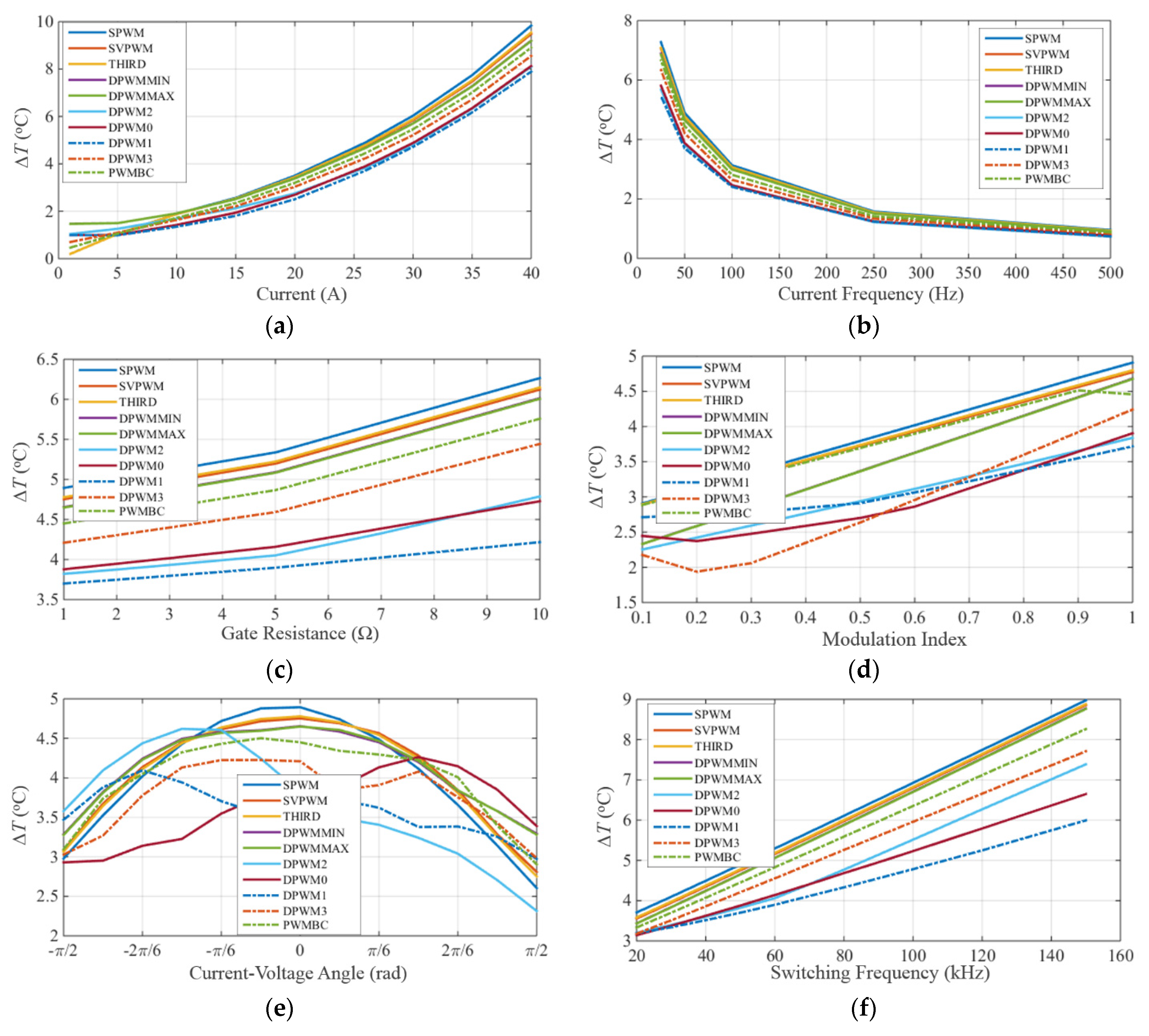
Figure 15 shows how this Δ
T changes with the value (a) and the frequency (b) of the fundamental current, the gate resistance of the SiC module (c), the modulation index
Mi (d), the angle between the current and the voltage
φ (e), and the switching frequency
Fsw (f). Parameters were fixed to those of the calculations shown in
Section 3.
Note that the DPWM1 method provided the lowest junction temperature variation, for all operating points, except for those with low levels of modulation index and an angle between voltage and current far from zero. Some of these conclusions are specific to the values taken as reference in this study. Obviously, different parameters and components can lead to different conclusions, but the approach shown here is valid.
ΔT significantly increased when increasing gate resistance, switching frequency, and output current, as well as when losses increased. On the other hand, a higher fundamental frequency of output current resulted in a lower ΔT. As a result, applications having the same fundamental frequency as that one in the existing internal aircraft electrical network (400 Hz) or high-speed motor drive applications (higher than 500 Hz) present lower ΔT, which increases power module lifetime, even if you have more thermal cycles per second. However, in aircraft applications such as inverters for future aircraft internal distribution systems (230 V/50 Hz) and low-speed motor drives, ΔT may be quite high, reducing power module lifetime.
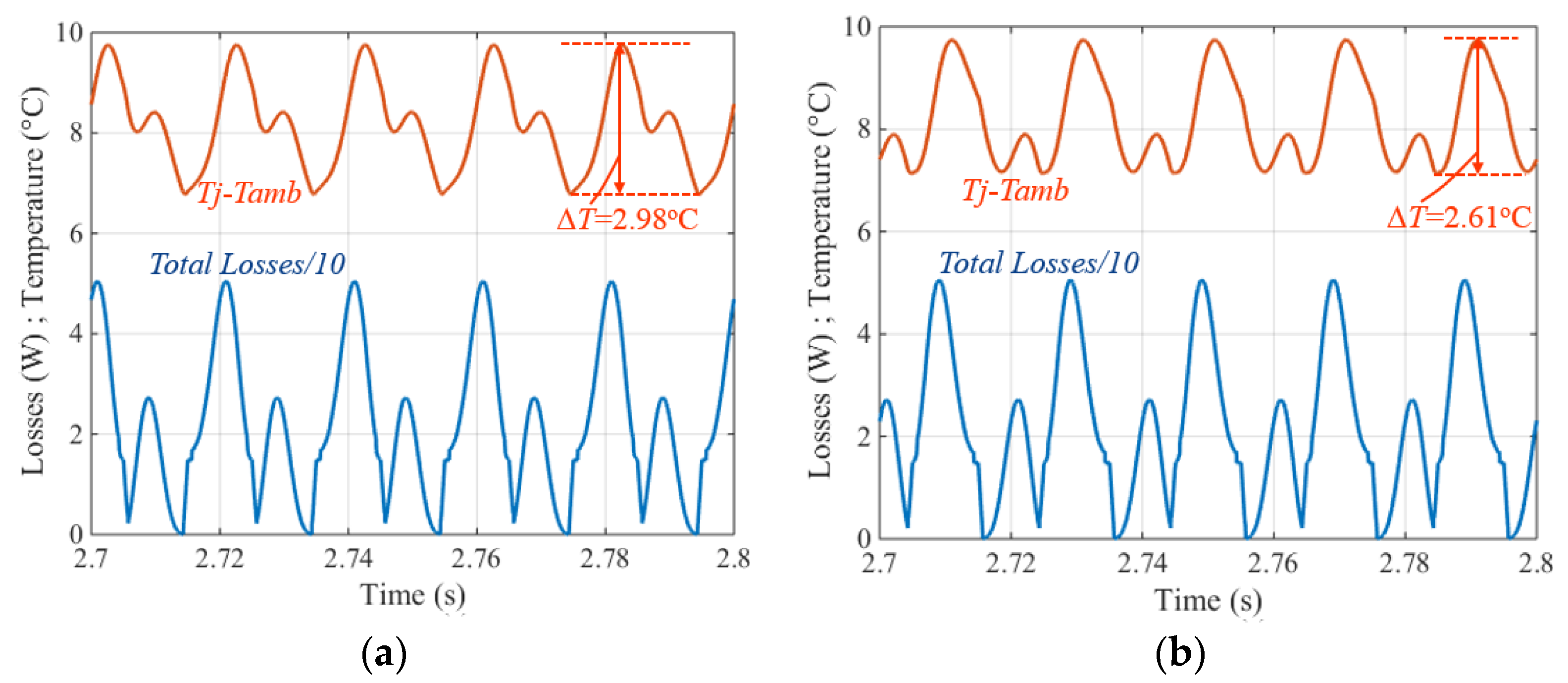
Another interesting conclusion from
Figure 15 is that different operation points resulted in different Δ
T for the same average losses, even if the instantaneous loss waveforms were the same, but mirrored. This is shown in
Figure 16, where we plotted five periods of these waveforms for the angles between the current and the voltage
φ of π and −π, for the SPWM modulation. Note that when the angle
φ was equal to π (pure capacitive load,
Figure 16a), the instantaneous loss waveform was mirrored when compared to when angle
φ was equal to −π (pure inductive load,
Figure 16b). Average losses were the same in both cases, but the instantaneous junction temperature had different waveforms, as well as different peak-to-peak values (∆
T).
In order to reduce converter losses and increase power module lifetime, a specific PWM method can be chosen or created, using, for example, algorithms as those shown in Reference [
8]. However, one must precisely know how to calculate conduction and switching losses, as well as dynamic junction temperature, as proposed in this paper.
7. Conclusions
This document focused on the analysis of temperature swing in the junction of SiC semiconductors used in a three-phase inverter connected to an aeronautic HVDC bus (at 540 V) intended to drive 15-kVA motors. This converter was based on a 1200-V/50-A SiC module from WOLFSPEED (reference CCS050M12CM2).
We presented a description of how PWM methods and other parameters directly influence losses and thermal cycling in a SiC device used in a 15-kVA three-phase inverter, which impact its reliability. Thanks to the precise characterization of the switching energies, the instantaneous losses of each component could be calculated. This allowed us to estimate thermal cycling of the SiC die junction and the gain in terms of lifetime for different parameters and PWM methods.
We showed precise models and calculations, as well as a complete analysis of the impact on the thermal cycling, not only of the PWM method, but also of the parameters of the load (angle, current, and fundamental frequency) and of the inverter (switching frequency, gate resistance of the transistors).
Theoretical results were compared to experimental results measured from the designed three-phase SiC inverter. This comparison showed differences between measured and calculated losses of around 5%, for any PWM method, for output power from 12 to 13.5 kVA, and for switching frequency of 50 kHz. At this switching frequency, the efficiency of the designed converter was around 99%, which shows the high performance of SiC MOSFETs in aircraft applications.
The calculation developed in this study shows that the junction temperature can be calculated for any operating point. Thus, after obtaining the reliability model of the SiC power module used in a converter, an accurate calculation of the number of cycles to failure is possible thanks to the approach shown in this paper.
It should be noted that, for the specific parameters used in this work, the DPWM1 modulation provides a lower temperature variation compared to other sinusoidal PWM modulation methods, except for low modulation index levels and voltage and current angles not equal to zero. Of course, the PWM method can be adapted and optimized to reduce the amplitude of these thermal cycles. This can be addressed in future work.
Author Contributions
Conceptualization, B.C. and G.S.; methodology, B.C.; software, B.C., H.T.D., and L.M.F.M.; validation, H.T.D.; investigation, B.C., H.T.D., and L.M.F.M.; writing—original draft preparation, B.C., L.M.F.M., and R.R.; writing—review and editing, B.C., L.M.F.M., and R.R.; supervision, B.C. All authors have read and agreed to the published version of the manuscript.
Funding
This research was funded by CAPES-COFECUB (876/2017), as well as by the members of the EPOWERDRIVE project at IRT, which are AKKA/Aeroconseil, Airbus, APSI3D, Liebherr Aerospace, Meggit/TFE Electronic, NIDEC/Leroy Somer, Safran E&P, Safran Tech, Zodiac Aeroelectric, and Zodiac Actuation Systems.
Conflicts of Interest
The authors declare no conflict of interest.
References
- Biela, J.; Schweizer, M.; Waffler, S.; Kolar, J.W. SiC versus Si—Evaluation of Potentials for Performance Improvement of Inverter and DC–DC Converter Systems by SiC Power Semiconductors. IEEE Trans. Ind. Electron. 2011, 58, 2872–2882. [Google Scholar] [CrossRef]
- Alves, W.C.; Morais, L.; Cortizo, P.C. Design of an Highly Efficient AC-DC-AC Three-Phase Converter Using SiC for UPS Applications. Electronics 2018, 7, 425. [Google Scholar] [CrossRef]
- Onambele, C.; Elsied, M.; Mabwe, A.M.; El Hajjaji, A. Multi-Phase Modular Drive System: A Case Study in Electrical Aircraft Applications. Energies 2017, 11, 5. [Google Scholar] [CrossRef]
- Cougo, B.; Schneider, H.; Meynard, T. Accurate switching energy estimation of wide bandgap devices used in converters for aircraft applications. In Proceedings of the 2013 15th European Conference on Power Electronics and Applications (EPE), Lille, France, 2–6 September 2013. [Google Scholar]
- Krismer, F.; Kolar, J.W. Accurate Power Loss Model Derivation of a High-Current Dual Active Bridge Converter for an Automotive Application. IEEE Trans. Ind. Electron. 2010, 57, 881–891. [Google Scholar] [CrossRef]
- Cougo, B.; Tran, D.-H.; Segond, G.; Hilal, A. Influence of PWM methods in semiconductor losses of 15kVA three-phase SiC inverter for aircraft applications. In Proceedings of the 2017 19th European Conference on Power Electronics and Applications (EPE’17 ECCE Europe), Warsaw, Poland, 11–14 September 2017. [Google Scholar]
- Hava, A.M. Carrier Based PWM - VSI Drives in the Overmodulation Region. Ph.D. Thesis, University of Wisconsin, Madison, WI, USA, 1998. [Google Scholar]
- Cougo, B.; Meynard, T.; Gateau, G.; Morais, L. Zero Sequences Optimizing Different Criteria for Three-Phase Multilevel Inverters. In Proceedings of the 2018 IEEE Energy Conversion Congress and Exposition (ECCE), Portland, OR, USA, 23–27 September 2018. [Google Scholar]
- Kaplar, R.J.; Marinella, M.J.; Dasgupta, S.; Smith, M.A.; Atcitty, S.; Sun, M.; Palacios, T. Characterization and reliability of SiC- and GaN-based power transistors for renewable energy applications. In Proceedings of the 2012 IEEE Energytech, Cleveland, OH, USA, 29–31 May 2012. [Google Scholar]
- Ueda, T. Reliability issues in GaN and SiC power devices. In Proceedings of the 2014 IEEE International Reliability Physics Symposium, Waikoloa, HI, USA, 1–5 June 2014. [Google Scholar]
- Dupont, L.; Coquery, G.; Kriegel, K.; Melkonyan, A. Accelerated active ageing test on SiC JFETs power module with silver joining technology for high temperature application. Microelectron. Reliab. 2009, 49, 1375–1380. [Google Scholar] [CrossRef]
- Masson, A.; Buttay, C.; Morel, H.; Raynaud, C.; Hascoet, S.; Gremillard, L. High-Temperature Die-Attaches for SiC Power Devices. In Proceedings of the 2011 14th European Conference on Power Electronics and Applications, Birmingham, UK, 30 August–1 September 2011. [Google Scholar]
- Batunlu, C.; Albarbar, A. A Technique for Mitigating Thermal Stress and Extending Life Cycle of Power Electronic Converters Used for Wind Turbines. Electronics 2015, 4, 947–968. [Google Scholar] [CrossRef]
- Scheuermann, U.; Junghaene, M. Limitation of Power Module Lifetime Derived from Active Power Cycling Tests. In Proceedings of the (CIPS 2018) 10th International Conference on Integrated Power Electronics Systems, Stuttgart, Germany, 20–22 March 2018; pp. 78–87. [Google Scholar]
- Hu, B.; Gonzalez, J.O.; Ran, L.; Ren, H.; Zeng, Z.; Lai, W.; Gao, B.; Alatise, O.; Lu, H.; Bailey, C.; et al. Failure and Reliability Analysis of a SiC Power Module Based on Stress Comparison to a Si Device. IEEE Trans. Device Mater. Reliab. 2017, 17, 727–737. [Google Scholar] [CrossRef]
- Mouawad, B. Assemblages Innovants en électronique de Puissance Utilisant la Technique de Spark Plasma Sintering. Ph.D. Thesis, Institut National des Sciences Appliquées de Lyon, Lyon, France, 2013. [Google Scholar]
- Testa, A.; De Caro, S.; Panarello, S.; Patanè, S.; Letor, R.; Russo, S.; Poma, S.; Patti, D. Stress analysis and lifetime estimation on power MOSFETs for automotive ABS systems. In Proceedings of the 2008 IEEE Power Electronics Specialists Conference, Rhodes, Greece, 15–19 June 2008; pp. 1169–1175. [Google Scholar]
- Zhang, Z.; Wang, F.; Tolbert, L.M.; Blalock, B.J.; Costinett, D. Evaluation of Switching Performance of SiC Devices in PWM Inverter-Fed Induction Motor Drives. IEEE Trans. Power Electron. 2015, 30, 5701–5711. [Google Scholar] [CrossRef]
- Cougo, B.; Schneider, H.; Meynard, T. High Current Ripple for Power Density and Efficiency Improvement in Wide Bandgap Transistor-Based Buck Converters. IEEE Trans. Power Electron. 2015, 30, 4489–4504. [Google Scholar] [CrossRef]
- Cougo, B.; Meynard, T.; Forest, F.; Laboure, E. Optimal PWM method for flux reduction in InterCell Transformers coupling double three-phase systems. Eur. J. Electr. Eng. 2010, 15, 23–38. [Google Scholar] [CrossRef]
- Kolar, J.W.; Krismer, F.; Lobsiger, Y.; Mühlethaler, J.; Nussbaumer, T.; Miniböck, J. Extreme Efficiency Power Electronics. In Proceedings of the 2012 7th International Conference of Integrated Power Electronics Systems (CIPS 2012), Nuremberg, Germany, 6–8 March 2012. [Google Scholar]
Figure 1.
Basic three-phase inverter connected to a load with floating neutral-point, used as reference in calculation of semiconductor losses and built for a test platform.
Figure 1.
Basic three-phase inverter connected to a load with floating neutral-point, used as reference in calculation of semiconductor losses and built for a test platform.
Figure 2.
Internal structure of a generic IGBT/MOSFET power module as shown in [
16].
Figure 2.
Internal structure of a generic IGBT/MOSFET power module as shown in [
16].
Figure 3.
Number of cycles to failure versus temperature variation of a MOSFET die in a power module for automotive applications, as shown in Reference [
17].
Figure 3.
Number of cycles to failure versus temperature variation of a MOSFET die in a power module for automotive applications, as shown in Reference [
17].
Figure 4.
Variation of on-state resistance RDSon with (a) junction temperature Tj and gate-source voltage Vgs (on the left), and (b) the SiC MOSFET current IDS (on the right). Figures were extracted from the reference SiC MOSFET power module datasheet (CCS050M12CM2).
Figure 4.
Variation of on-state resistance RDSon with (a) junction temperature Tj and gate-source voltage Vgs (on the left), and (b) the SiC MOSFET current IDS (on the right). Figures were extracted from the reference SiC MOSFET power module datasheet (CCS050M12CM2).
Figure 5.
(a) Instantaneous values of conduction losses in the top and bottom switches of one bridge leg of a three-phase inverter; (b) instantaneous values averaged over a switching period. Parameters were VDC = 540 V, Iout = 26.3 A, φ = 0°, Mi = 1, Fsw = 50 kHz. The pulse width modulation (PWM) method used was sinusoidal (SPWM).
Figure 6.
Experimental switching energy of the CCS050M12CM2 SiC module from Wolfspeed, as a function of switching current and voltage.
Figure 6.
Experimental switching energy of the CCS050M12CM2 SiC module from Wolfspeed, as a function of switching current and voltage.
Figure 7.
Instantaneous values of (a) switching losses averaged in a switching period and (b) total (conduction + switching) losses in the top and bottom switches of one bridge leg of a three-phase inverter having VDC = 540 V, Iout = 26.3 A, φ = 0°, Mi = 1, Fsw = 50 kHz. The modulation method used was sinusoidal (SPWM).
Figure 8.
Instantaneous values of (a) conduction, (b) switching, and (c) total (conduction + switching) losses in the top and bottom switches of one bridge leg of a three-phase inverter having: VDC = 540 V, Iout = 26.3A, φ = 0°, Mi = 1, Fsw = 50 kHz. The modulation method used was DPWM1.
Figure 8.
Instantaneous values of (a) conduction, (b) switching, and (c) total (conduction + switching) losses in the top and bottom switches of one bridge leg of a three-phase inverter having: VDC = 540 V, Iout = 26.3A, φ = 0°, Mi = 1, Fsw = 50 kHz. The modulation method used was DPWM1.
Figure 9.
Total semiconductor losses versus (a) value and (b) frequency of the fundamental current, (c) the gate resistance of the SiC module, (d) the modulation index Mi, (e) the angle between the current and the voltage φ, and (f) the switching frequency Fsw. Fixed parameters were VDC = 540 V, Iout = 26.3 A, φ= 0°, Mi = 1, Fsw = 50 kHz, Rg = 10 Ω, Vgs = −4 V/20 V, DT = 400 ns, and fundamental frequency = 50 Hz.
Figure 10.
Three-phase inverter using SiC power module verify loss calculation in a 15-kVA/540-V application.
Figure 10.
Three-phase inverter using SiC power module verify loss calculation in a 15-kVA/540-V application.
Figure 11.
Experimental set-up to measure losses in three-phase SiC inverter.
Figure 11.
Experimental set-up to measure losses in three-phase SiC inverter.
Figure 12.
Loss estimation for each part of the converter based on measured losses: (a) losses using SPWM method at output power of 13.6 kVA; (b) losses using DPWM1 method at output power of 14.5 kVA.
Figure 12.
Loss estimation for each part of the converter based on measured losses: (a) losses using SPWM method at output power of 13.6 kVA; (b) losses using DPWM1 method at output power of 14.5 kVA.
Figure 13.
Thermal impedance between the SiC MOSFET junction and the SiC power module case (reference CCS050M12CM2).
Figure 13.
Thermal impedance between the SiC MOSFET junction and the SiC power module case (reference CCS050M12CM2).
Figure 14.
Thermal resistance and capacitance network representing the thermal impedance between the SiC MOSFET junction and SiC power module case (reference CCS050M12CM2).
Figure 14.
Thermal resistance and capacitance network representing the thermal impedance between the SiC MOSFET junction and SiC power module case (reference CCS050M12CM2).
Figure 15.
Amplitude of the variation of the junction temperature versus (a) value and (b) the frequency of the fundamental current, (c) the gate resistance of the SiC module Rg, (d) the modulation index Mi, (e) the angle between the current and the voltage φ, and (f) the switching frequency Fsw. Fixed parameters were VDC = 540 V, Iout = 26.3 A, ϕ = 0°, Mi = 1, Fsw = 50 kHz, Rg = 10 Ω, Vgs = −4 V/20 V, DT = 400 ns, and fundamental frequency = 50 Hz.
Figure 16.
Instantaneous losses (bottom curves) and junction temperature variation (upper curves) for different angles between the current and the voltage (φ): (a) φ = −π; (b) φ = +π. Although average losses are the same and loss waveforms are the same (but mirrored), the junction temperatures have different waveforms and amplitudes for these two angles.
Table 1.
Calculated and measured total losses of three-phase inverter at around 12 kVA (for continuous PWM methods) and 13.5 kVA (for discontinuous PWM methods), with Fsw = 50 kHz.
Table 1.
Calculated and measured total losses of three-phase inverter at around 12 kVA (for continuous PWM methods) and 13.5 kVA (for discontinuous PWM methods), with Fsw = 50 kHz.
| | SPWM | SVPWM | THI
PWM | DPWM
MIN | DPWM
MAX | DPWM
0 | DPWM
1 | DPWM
2 | DPWM
3 | PWM
BC |
|---|
| Measured (W) | 154 | 155 | 154 | 128 | 131 | 133 | 127 | 126 | 132 | 145 |
| Calculated (W) | 146 | 146 | 146 | 123 | 123 | 127 | 120 | 118 | 126 | 138 |
| Difference (W) | 8 | 9 | 8 | 5 | 8 | 6 | 7 | 8 | 6 | 7 |
| Difference (%) | 5.2 | 5.8 | 5.2 | 3.9 | 6.1 | 4.5 | 5.5 | 6.4 | 4.6 | 4.8 |
Table 2.
Thermal resistance and capacitance values representing the thermal impedance between the SiC MOSFET junction and the SiC power module case (reference CCS050M12CM2).
Table 2.
Thermal resistance and capacitance values representing the thermal impedance between the SiC MOSFET junction and the SiC power module case (reference CCS050M12CM2).
Thermal Resistance
(K/W) | Thermal Capacitance
(J/K) |
|---|
| R0 | 4.18 × 10⁻³ | C0 | 3.07 × 10⁻³ |
| R1 | 7.49 × 10⁻³ | C1 | 7.93 × 10⁻³ |
| R2 | 7.33 × 10⁻² | C2 | 1.89 × 10⁻² |
| R3 | 1.41 × 10⁻² | C3 | 9.41 × 10⁻³ |
| R4 | 5.83 × 10⁻² | C4 | 4.42 × 10⁻² |
| R5 | 4.24 × 10⁻² | C5 | 5.33 × 10⁻² |
| R6 | 2.80 × 10⁻² | C6 | 8.55 × 10⁻² |
| R7 | 2.30 × 10⁻² | C7 | 1.87 × 10⁻¹ |
| R8 | 2.40 × 10⁻² | C8 | 3.64 × 10⁻¹ |
| R9 | 2.42 × 10⁻² | C9 | 6.51 × 10⁻¹ |
| R10 | 2.33 × 10⁻² | C10 | 1.22 |
| R11 | 2.21 × 10⁻² | C11 | 2.47 |
| R12 | 1.86 × 10⁻² | C12 | 5.01 |
| R13 | 6.80 × 10⁻³ | C13 | 25.1 |
© 2020 by the authors. Licensee MDPI, Basel, Switzerland. This article is an open access article distributed under the terms and conditions of the Creative Commons Attribution (CC BY) license (http://creativecommons.org/licenses/by/4.0/).


