Article

Thermoelectric Performance Enhancement of Naturally Occurring Bi and Chitosan Composite Films Using Energy Efficient Method

1
Department of Mechanical Engineering, University of Maryland, Baltimore County, Baltimore, MD 21250, USA
2
Department of Mechanical and Aerospace Engineering, University of Virginia, Charlottesville, VA 22904, USA
3
Department of Materials Science and Engineering, University of Virginia, Charlottesville, VA 22904, USA
4
Department of Physics, University of Virginia, Charlottesville, VA 22904, USA
*
Author to whom correspondence should be addressed.
Electronics 2020, 9(3), 532; https://doi.org/10.3390/electronics9030532
Submission received: 1 February 2020 / Revised: 13 March 2020 / Accepted: 16 March 2020 / Published: 23 March 2020
(This article belongs to the Special Issue Energy Harvesting and Storage Applications)

Abstract

:
This work presents an energy efficient technique for fabricating flexible thermoelectric generators while using printable ink. We have fabricated thermoelectric composite thick films using two different mesh sizes of n-type bismuth particles, various binder to thermoelectric material weight ratios, and two different pressures, 200 MPa and 300 MPa, in order to optimize the thermoelectric properties of the composite films. The use of chitosan dissolved in dimethylsulfoxide with less than 0.2 wt. % of chitosan, the first time chitosan has been used in this process, was sufficient for fabricating TE inks and composite films. Low temperature curing processes, along with uniaxial pressure, were used to evaporate the solvent from the drop-casted inks. This combination reduced the temperature needed compared to traditional curing processes while simultaneously increasing the packing density of the film by removing the pores and voids in the chitosan-bismuth composite film. Microstructural analysis of the composite films reveals low amounts of voids and pores when pressed at sufficiently high pressures. The highest performing composite film was obtained with the weight ratio of 1:2000 binder to bismuth, 100-mesh particle size, and 300 MPa of pressure. The best performing bismuth chitosan composite film that was pressed at 300 MPa had a power factor of 4009 ± 391 μW/m K2 with high electrical conductivity of 7337 ± 522 S/cm. The measured thermal conductivity of this same sample was 4.4 ± 0.8 W/m K and the corresponding figure of merit was 0.27 at room temperature.

1. Introduction

As the rate of energy consumption continues its rapid growth, energy conversion processes are facing a great challenge to meet the demand. When considering that the majority of energy is wasted in the form of heat during device and machine operations (e.g., automobile engines, power transistors, light bulbs, industrial processes, etc.), energy harvesting devices, such as a thermoelectric generator (TEG), can be used to convert the waste heat into electricity [1,2,3]. The long lifespan of TEGs, coupled with fewer replacement requirements than other devices, such as solar cells, make it an attractive technology for energy harvesting. To date, TEGs have been applied in a vast number of areas, including wireless sensor networks, various medical fields, wearable devices, industrial, military, and remote monitoring systems [4,5]. The conventional manufacturing of TEGs dices an ingot of bulk material and, subsequently, assembles and integrates the diced piece. The conventional pick-and-place methods for thermoelectric device manufacturing are limited to low aspect-ratio elements and the associated micro-fabrication technology has a limited cost-effective scalability. Additive methods, such as dispenser printing, screen printing, stencil printing, and inkjet printing, have been introduced to overcome the conventional method’s limitations, due to the disadvantages of this method. Previous research has shown that these additive methods promise a simple, cost-effective, and scalable way to manufacture TEGs [6,7,8,9].
The theoretical maximum efficiency of the energy conversion process for a thermoelectric (TE) material is determined by the figure of merit, ZT, as given by
ZT = σ α 2 T κ
where σ is the electrical conductivity, α is the Seebeck coefficient, T is the temperature, and κ is the total thermal conductivity from both electronic and phononic contributions [3,10,11]. The thermoelectric material with high electrical conductivity and high Seebeck coefficient paired with low thermal conductivity can achieve a high figure of merit. However, the achievement of high ZT is challenging because of the factors in ZT, the electrical conductivity, the Seebeck coefficient, and the thermal conductivity, are determined by the natural properties of the material itself property. The electrical conductivity and the Seebeck coefficient for TE materials are roughly inversely proportional, due to their relationship to carrier concentration [12,13]. In addition, materials with high electrical conductivity generally have high thermal conductivity, due to electrons carrying a large amount of heat. Thus, numerous pathways for improving the ZT of thermoelectric materials, such as doping, and structural (nano material) methods, have been pursued [4,14,15,16,17,18,19,20,21,22].
Thermoelectric inks that are made from the combination of thermoelectric materials and binders have enabled their use in the additive manufacturing process. The use of a binding agent enables the solution process, prior to curing, and helps to maintain the thermoelectric particles in the form of a thin film via adhesion between particles and the surrounding binding material. Various types of materials have been applied as binders for thermoelectric films, such as removable binders [5,7,8,23,24], thermoset polymers [4,17,22,25,26,27], and biomaterials [28]. Large amounts of binder residue when using epoxy resins in TE composite films reduce electrical conductivity, and epoxy resins require high temperatures and long times to cure [29]. Madan et al. used various sintering methods and added different additives to obtain a maximum ZT of 0.41 for p-type epoxy binding TE composite films [4]. Other research groups used removable binder and achieved higher ZT for both p- and n-type TE films in order to improve the electrical conductivity of TE-epoxy composite films, but they could not eliminate the curing process that requires both high temperature and long cure times [7,8,30,31]. A new biomaterial, nano-fibrous cellulose (NFC), was introduced as a binder for thermoelectric by Jang et al. and showed that the nano-fibrous cellulose material was an excellent binder for thermoelectric composite films [28]. Small amounts of NFC binder had high enough adhesive strength to hold the TE particles and, thus, reduced the electrically insulating binder content in the TE composite films, which led to high electrical conductivity at room temperature.
Pressing methods during the curing process have been shown to increase the density of composite films. Cao et al., Choi et al., and other research groups showed, via scanning electron microscope (SEM) imaging after pressing, better alignment, closer particle distance, and greater contact between active particles, which, in theory, would demonstrate better electrical conductivity [7,8,26,27]. However, they used the pressing method during and after a lengthy high temperature cure. Jang et al. also introduced pressing as the post annealing method in order to densify their composite films. In the Jang et al. study, the pressing method not only increased the density of the film, but also eliminated pores, voids, and the highly energy intensive curing process. The pressed denser films had higher electrical conductivity without using the energy intensive steps [28].
Various research groups have investigated the effect of grain size on the properties of bulk TE materials. If the particle size is small enough, electrical conductivity has been shown to significantly decrease due to the potential barrier scattering at the grain boundary [32]. Small particle sizes form a potential barrier, such that a charge carrier without sufficient energy could not jump over the potential barrier, subsequently lowering the electrical conductivity [33]. Takashiri et al. reported that, as the grain size decreased, the number of defects at the grain boundary increased, and this results in lower electrical conductivity and a sharp decrease in the figure of merit ZT [34]. However, to the best of our knowledge, no one has reported the particle size effects on the TE properties of printed TE composite films.
This study reports an experimental study undertaken to understand the effect of TE particle size on the electrical conductivity of composite TE films. In this work, we employed two different mesh sizes of bismuth particles (100-mesh and 200-mesh) and mixed the naturally occurring chitosan binder to prepare the TE inks. The absence of water in with the DMSO-chitosan makes the composite films more stable due to less oxidation issues. The external applied pressure helped to densify the films and eliminate pores and voids. The characterization of thermoelectric properties with respect to various fabrication conditions, such as mesh size (100-mesh and 200-mesh), pressure (200 MPa and 300 MPa), and binder to TE material weight ratio (1:500, 1:1000, 1:2000, and 1:5000) was demonstrated. We successfully made high performing chitosan-bismuth composite TE films and their electrical conductivity and Seebeck coefficient values were comparable to the values of bulk bismuth [35,36]. The scanning electron microscope (SEM) images and density measurements confirmed that the chitosan-bismuth composite films had bulk-like structure. The achievement of bulk like structure in n-type TE composite films drastically improved the electrical conductivity of the chitosan-bismuth composite TE films and resulted in high power factors.

2. Materials and Methods

Commercially available 100-mesh bismuth particles (Santech Inc., China) and 200-mesh bismuth particles (Fisher scientific) were used as the TE material without further purification and grinding. Chitosan (MP Biomedicals, LLC) and dimethyl sulfoxide (DMSO, 99.7+%, extra dry, ACROS Organics) were purchased and used as received. In order to synthesize the chitosan binder, 98.4 mg of salicylic acid particle (Fisher scientific, >99%) was added to 15 mL of DMSO and then mixed with a vortex mixer until the salicylic acid particles were completely dissolved. For the thicker chitosan binder, 150 mg of chitosan powder was added to the DMSO blend, and, for the light chitosan binder, 50 mg of chitosan powder was added to the DMSO blend. While using a vortex mixer, agglomerated chitosan was dispersed, and, for complete dissolution, the binder solution was placed on a hot plate with magnetic stirring at 75 °C and 300 rpm overnight. Four different weight ratios of binder to TE particles, 1:500, 1:1000, 1:2000, and 1:5000, were synthesized. For the 1:5000 ratio ink, an additional amount of DMSO was added to attain the proper viscosity to drop cast the film. Inks were mixed using a vortex mixer for one minute and then sonicated in an ultrasonic bath for 30 min in order to achieve homogeneity.
Chitosan coated Kevlar (Fiber Glast Development Corp., KEVLAR® Plain Weave Fabric) was chosen as the substrate. Chitosan coatings that are made the Kevlar attain a more uniform surface, as described in previous work [28]. Mixtures of 0.1 M of acetic acid (Fisher Chemical, ≥99.7 w/w %) and 150 mg of chitosan were added to 15 mL of deionized (DI) water and then magnetically stirred on a hot plate as before to obtain diluted chitosan. The diluted chitosan was applied to the kevlar substrates and the coated substrates were dried overnight. The TE films were made by drop casting the homogeneous inks on a chitosan coated kevlar substrate and the diameters of the deposited TE inks were approximately 5 mm. The deposited inks were cured at 120 °C for 10 min in an oven until solvent evaporation was complete. After the drying of the inks, external pressures (200 and 300 MPa) were applied to the cured films. A hydraulic press (MTI corp., YLJ-CSP-30) applied pressure to the films for five minutes. The applied pressure was calibrated and determined in a previous work from our research group [28]. A polyethylene film was placed on top of the TE films to protect the TE films during the pressing.
A Hall Effect measurement system (ECOPIA, HMS-5500) was employed in order to measure the electrical conductivity and charge carrier concentration. Multiple TE films were fabricated from each TE ink and measured TE properties to reduce the error. The average of all the results was used and all of the measurements were performed in ambient air. Prior to electrical conductivity measuring, a vernier caliper (Mityutoyo, 293-340-30) was used to measure the thickness of the sample. The TE films thickness (200~300 μm) was obtained by calculating the difference between substrate thickness (250 μm) and whole thickness (450~550 μm). A custom-built Seebeck measurement setup was used to measure the Seebeck coefficient. Two peltiers were used to generate temperature differences (0 K, 2 K, 4 K, and 6 K) across the sample by applying various voltages (0 V, 0.7 V, 1.4 V, and 2.1 V) to the peltiers. Each stage was given 65 s to stabilize the temperature between the peltiers and the TE films. A gold tip probe and a thermocouple were used on each of the ends of the sample in order to measure the voltage differences (ΔV) and the temperature differences (ΔT), respectively, across the sample. Multiple measurements (50 times at each different temperature stage) of both voltages and temperatures were recorded to minimize the error. The Seebeck coefficient was then calculated as the slope of the ΔT (x-axis) and ΔV (y-axis) straight line.
The scanning electron microscope (SEM) images of bismuth chitosan composite films were taken while using Nova NanoSEM 450. Particle size analysis was performed using scanning electron microscope (SEM) Nova NanoSEM 450 and ImageJ program. Bismuth particles of specific mesh were sprinkled on carbon tape. SEM images were taken at 500µ resolution to prepare samples for particle-size analysis. Image processing program ImageJ was used to analyze the number of particles of different sizes for different mesh Bi particles. The menu “Analyze particles” was used to count the number of the particles by different particle sizes. The density of the TE films was calculated with the measured films’ weight and volume. TE film’s weight was measured with a balance (SARTORIUS, TE214S Analytical Balance) and the volume was measured with a three-dimensional (3D) laser scanning microscope (KEYENCE, VX-X1000). The densities of the films were calculated by dividing the measured weight with the measured volume.
Thermal conductivity measurements were performed using the optical pump-probe technique steady-state thermoreflectance, described in detail below in Section 3.8 [37].

3. Results and Discussion

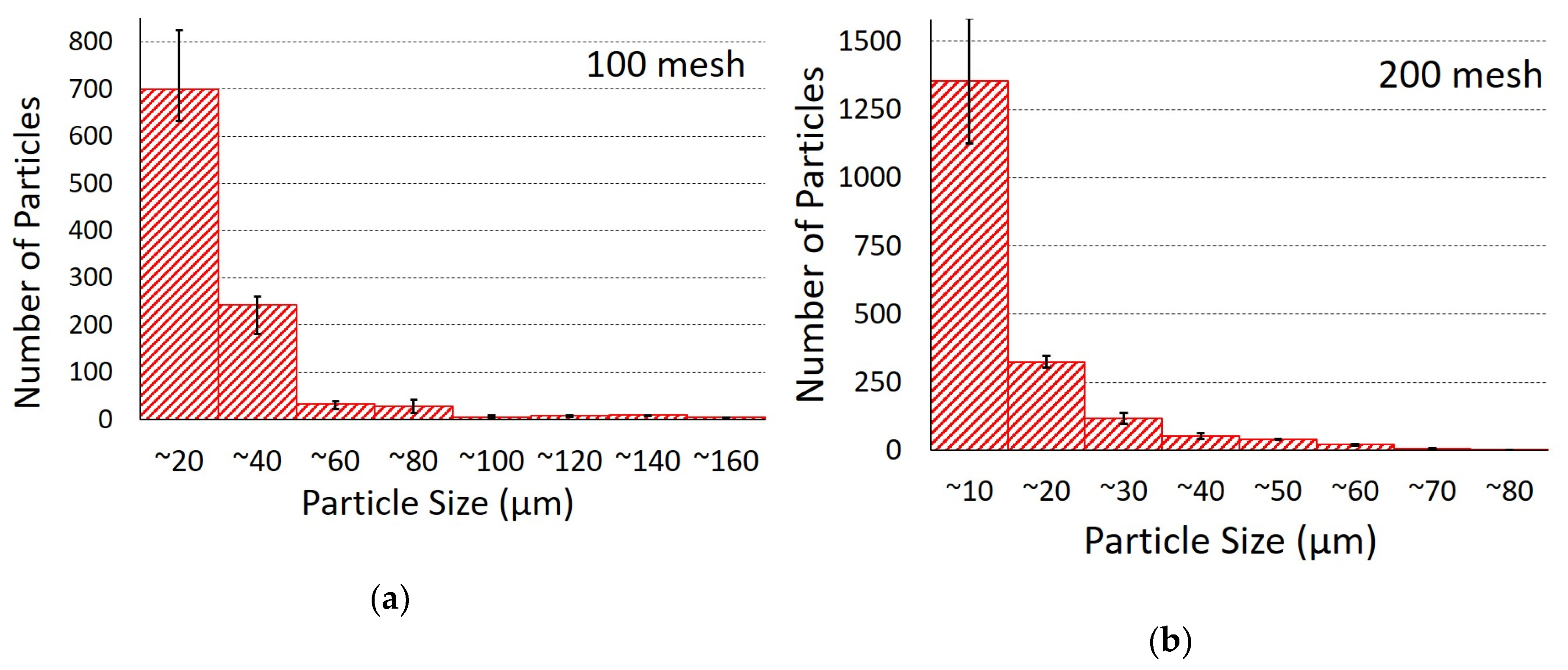
3.1. Particle Size Anaysis

Two different particle sizes of n-type bismuth particle (100-mesh and 200-mesh) were used to fabricate chitosan-bismuth composite films. Prior to preparing the inks, SEM was performed on the purchased bismuth particles. We took SEM images for 200-mesh and 100-mesh Bi particles at 650× (200 micron scale bar) and 250× (500 micron scale bar) magnification, as shown in Figure 1a–d. Figure 1 shows the SEM images of the particle distribution for bismuth particles-mesh size of 100 and 200. Figure 1a,c show the 100-mesh bismuth particles and are clearly composed of a larger distribution of particle sizes, submicron to ~150 μm, than the 200-mesh particles, which are in the order of submicron to ~80 μm. We used these SEM images and the ImageJ program to calculate the number of particles for different particles sizes. Figure 2a,b show particle counts (including the errors bars) corresponding to different particle sizes for all of the samples. Figure 2 shows that the 100-mesh bismuth particles have a wider distribution of particle sizes, while the 200-mesh bismuth particles have a more uniform fine particle size distribution.

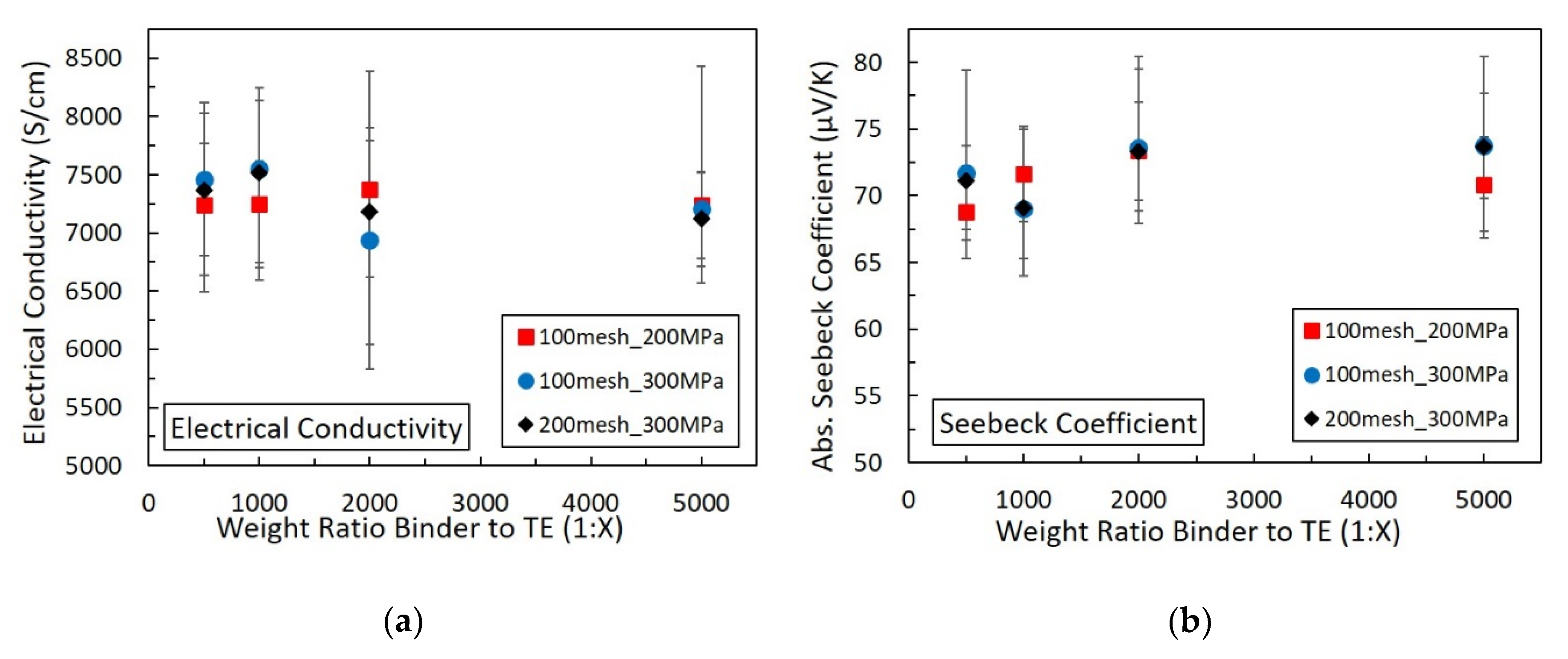
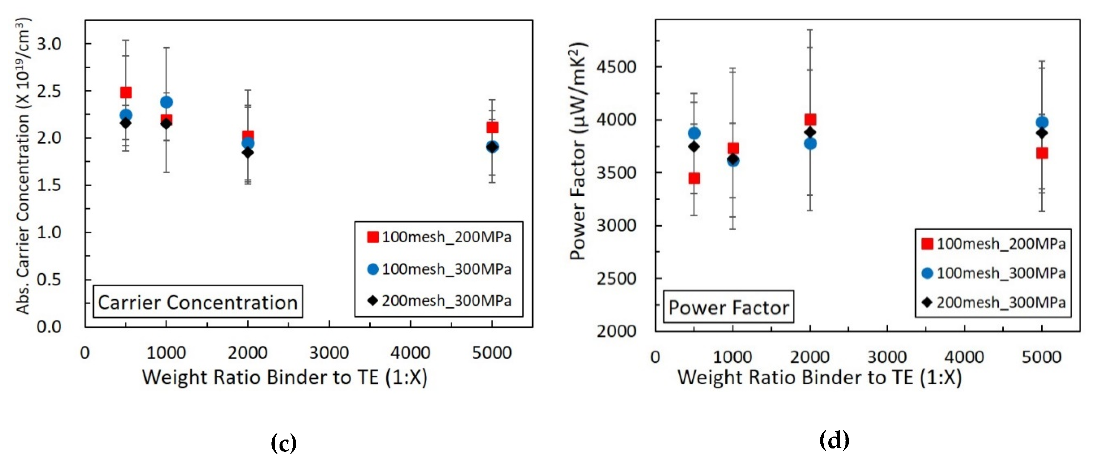
3.2. Thermoelectric Performance

Figure 3 presents the thermoelectric properties of the 200-mesh bismuth-chitosan composite films that were pressed at 300 MPa (black diamond) and the 100-mesh bismuth-chitosan composite films pressed at 200 MPa (red square) and 300 MPa (blue circle). First, we measured the thermoelectric properties of 100-mesh films. We conducted thermoelectric measurements for 200-mesh films only at the applied pressure of 300 MPa because we did not see any effect of applied pressure on thermoelectric properties for the 100-mesh films. The measured electrical conductivity, the absolute value of Seebeck coefficient, the absolute value of carrier concentration, and the calculated power factor are shown for the four different weight ratios between the binder and bismuth.

3.3. Electrical Conductivity

In Figure 3a, the highest electrical conductivity value (7550 ± 520 S/cm) was obtained from the 1:1000 binder to 100-mesh bismuth weight ratio TE composite films that were pressed at 300 MPa. The lowest electrical conductivity value (6940 ± 540 S/cm) was obtained from the 1:2000 binder to 100-mesh bismuth weight ratio TE composite films pressed at 300 MPa. We also pressed 200-mesh 1:500 weight ratio of binder to particles at 5 MPa and 50 MPa and the electrical conductivity was (871 ± 220 S/cm) and (4770 ± 670 S/cm), respectively. The electrical conductivity of the TE films that were pressed with higher pressure (≥100 MPa) was much higher and, as a result, we used higher pressures of 200 MPa and 300 MPa to maximize the electrical conductivity.
The electrical conductivity values were observed to be similar through all of the various weight ratios of binder to bismuth (1:500, 1:1000, 1:2000, and 1:5000) for different mesh size films and at different pressure. This phenomenon can be explained on the basis of the percolation theory of composite materials. Once the fraction of conductive material hits the percolation threshold, the conductive path forms in the composite material and electrical conductivity drastically increases [38,39]. In our previous work, we have shown that, for a 1:100 weight ratio of binder to TE material, the electrical conductivity was much lower than other two higher weight ratios of 1:1000 and 1:10,000 [28]. This suggests that the percolation threshold lies between 1:100 and 1:500 weight ratio of binder to active material. Therefore, in this work, we have chosen four different weight ratios (1:500, 1:1000, 1:2000, and 1:5000) and the electrical conductivity results suggest that they are all above the percolation threshold. The error range is comparable to similar films that were reported in the literature. It is typical to observe large errors in such films, due to the small size of the sample [14]. The electrical conductivity values did not change much by increasing the pressure from 200 MPa to 300 MPa, implying that 200 MPa of pressure was sufficient for densifying the films and reduce pores and voids. Similarly, the use of 100-mesh versus 200-mesh particles did not play much of a role in altering the electrical conductivity of the TE composite films. Overall, we have increased electrical conductivity in all different TE composite films to a level similar to bulk Bi electrical conductivity 8333–8900 S/cm [35,36] through use of the high binder to particle ratios, and the application of pressure after the curing step.

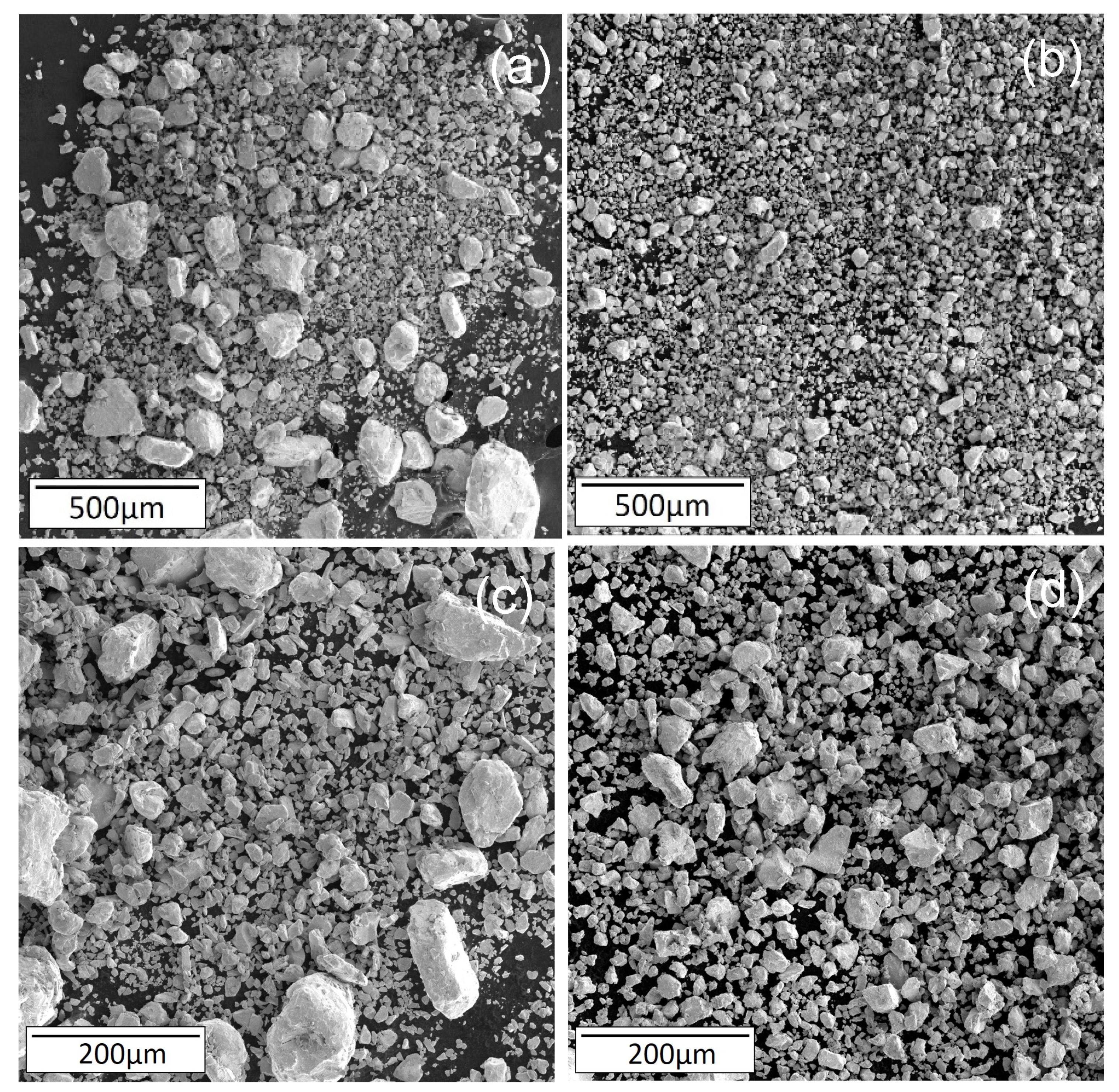
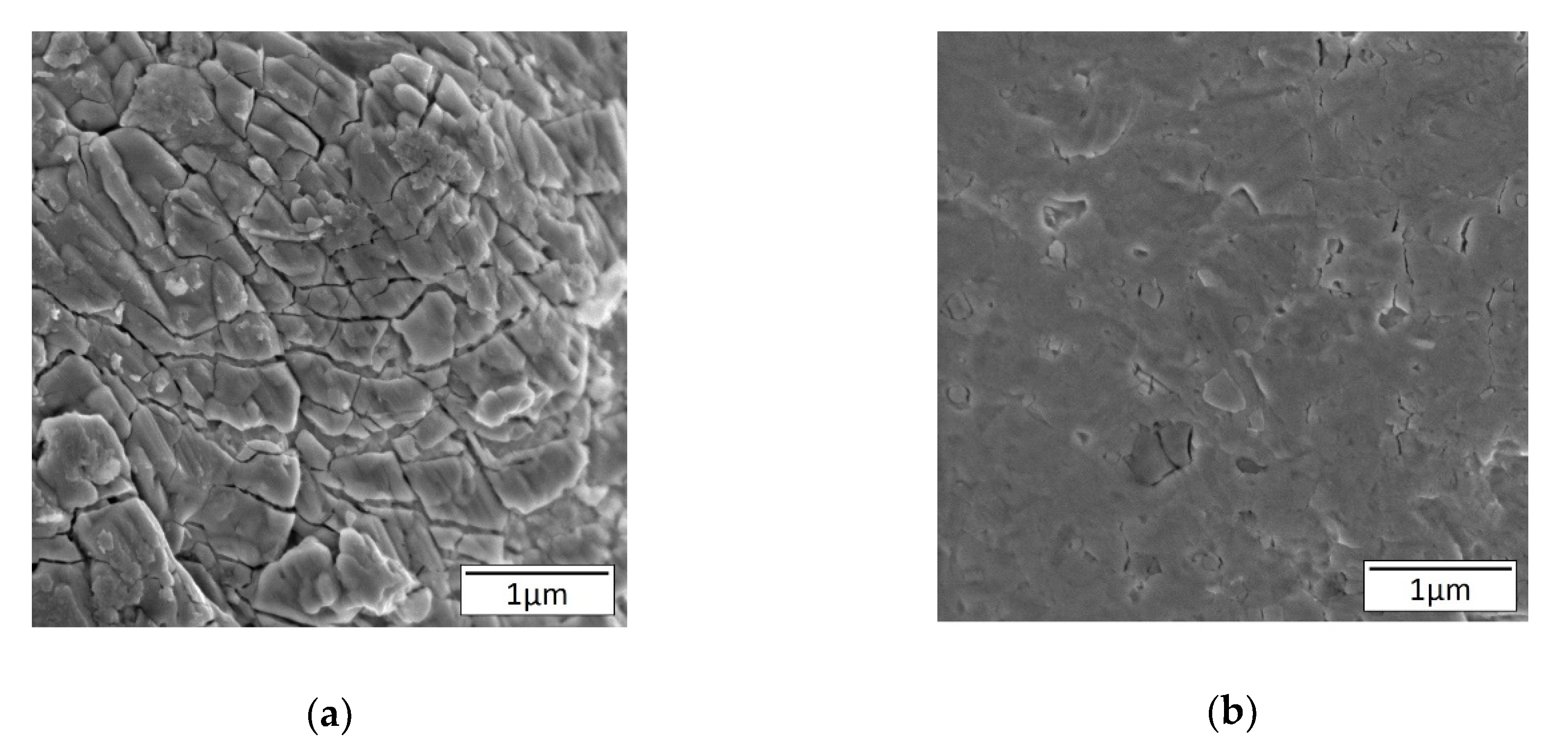
3.4. Microstructure Anaysis

We performed SEM of TE composite films with 1:2000 wt. ratio of binder to 100-mesh Bi particle at 300 MPa to understand the effect of pressure on electrical conductivity. Figure 4b shows the cross-sectional SEM images. For comparison purposes, we have performed SEM on 1:500 wt. ratio of binder to 100-mesh Bi particles composite films at low pressure (5MPa). Figure 4a shows the cross-sectional SEM images. The reason of choosing very low-pressure (5MPa) in contrast to high pressure (300 MPa) is that we wanted to see the grain and grain boundaries orientation in TE composite films under the application of low and high pressure. Under the application of low pressure 5MPa, we can easily see many grains and grain boundaries as shown in Figure 4a which result in charge carrier scattering and resulted in low electrical conductivity 870 S/cm. The applied external pressure facilitates particle coalescence and the formation of a bulk like structure since Bi is a ductile metal. However, it is interesting to note that both 100-mesh and 200-mesh Bi composite films have comparable electrical conductivity at high external applied pressure (200 MPa and 300 MPa). Moreover, the electrical conductivity was high for chitosan Bi TE composite films (100-mesh and 200-mesh) at 200 MPa and 300 MPa and the same as Bi bulk material [35,36]. The external applied pressure helped to densify the films and remove the pores and voids. Therefore, the electrical conductivity for different mesh and different weight ratio TE composite films has high electrical conductivity.

3.5. Density

We also performed density measurement on TE composite films of 1:2000 (weight ratio binder to 100-mesh Bi) at 200 MPa. The measured density of this TE composite film was 9.5 g/cm2 and the reported density of bulk bismuth is 9.78 g/cm2. Our composite film values are comparable to bulk Bi values, again confirming that particles were packed very well and resulted in bulk like structure and that led to high electrical conductivity [36].

3.6. Seebeck Coefficient

Figure 3b shows the measured absolute value of Seebeck coefficients of various TE composite films. The highest absolute Seebeck coefficient value (74 ± 5 μV/K) was obtained from the 1:5000 binder to 100-mesh bismuth weight ratio TE composite films pressed at 300 MPa. Since Bi is n-type material, the measured Seebeck coefficients of the composite films were negative. Actually, the Seebeck coefficient values are very similar to each other for different-mesh size and different weight ratio TE composite films. We did not find any trend in TE composite films by varying the grain size or weight ratio or external pressure. The particle size has no significant effect on the electrical conductivity and Seebeck coefficient of the film, as shown in Figure 3. This is because the application of pressure on ductile Bi resulted in similar plate-like structure, regardless of the starting particle size. The overall Seebeck coefficient that was obtained from this study was −68 μV/K to −74 μV/K and this value is almost same to that of bulk bismuth (−72 μV/K) [36]. However, Madan et al. fabricated epoxy-bismuth composite films and their Seebeck values were 10 μV/K higher than ours [25]. This can be explained because the epoxy-bismuth composite film contained a high amount of insulating binder and the electrical conductivity of their composite films were much lower than ours and their Seebeck coefficient values were slightly higher.

3.7. Power Factor

Figure 3c shows the measured absolute values of charge carrier concentration. The power factor of each TE film was calculated with the equation, Pf = α 2 × σ , and the averages of the power factor of various combinations are plotted in the Figure 3d. The overall power factor values were relatively similar. The highest power factor value (4010 ± 390 μW/m·K2) was obtained from the 1:2000 binder to 100-mesh bismuth weight ratio TE composite film that was pressed at 300 MPa. However, no significant difference was observed in terms of power factor by changing the weight ratio, grain size, or external applied pressure. The overall power factor of chitosan-bismuth TE composite films was in the range of 3500–4000 μW/m·K2. This value is two orders of magnitude higher than epoxy-bismuth composite films [25]. In this work, we use the energy efficient method to achieve high electrical conductivity in contrast to other reported work for composite films and achieved electrical conductivity that was similar to bulk values. Based on the electrical conductivity and the Seebeck values of bulk bismuth [35,36], the power factor of chitosan-bismuth composite films in this work should be similar to that of bulk bismuth.

3.8. Thermal Conductivity

The thermal conductivity of four chitosan-bismuth TE composite films with weight ratio of 1:2000 binder to 100-mesh Bi particles at 300 MPa were measured by non-contact, optical pump-probe technique steady-state thermoreflectance (SSTR) [37]. SSTR uses Fourier’s law to determine the thermal conductivity of a material by varying the incident pump power (proportional to heat flux) on the sample surface and detecting the reflectance change (proportional to temperature rise) [40,41] by a probe laser. The pump laser used in the SSTR set-up was a 532 nm continuous wavelength (CW) laser, whereas the probe laser was a 786 nm CW diode laser. Before the SSTR measurements, a thin Al layer was deposited on top of the sample surface by electron beam evaporation to convert the optical energy into thermal energy. The SSTR measurements were conducted using a sapphire wafer as a calibration to determine the experimental proportionality constant ϒ according to the procedure that was described in Braun et al. (2019). For each sample, the measurements were repeated with two different objectives (5× and 10×). The coaxially focused pump and probe laser 1/e2 diameters for each objective were nearly equal; ~20 and 44 μm for 10× and 5×, respectively.
We measured the thermal conductivity of 100-mesh and 325-mesh bismuth-chitosan composite films and find that the values for both samples were comparable (4.4 ± 0.8 W/m·K for 100-mesh film and 4.5 ± 0.8 W/m·K for 325-mesh film). This is because the application of pressure on ductile Bi resulted in a similar plate-like structure, regardless of starting particle size. Therefore, the particle size has no effect on the thermal conductivity of composite films of different applied pressure. The thermal conductivity value of 100-mesh Bi composite films is much lower than that of bulk thermal conductivity. The lower thermal conductivity of the composite was caused by the presence of insulating binder, nano scale defects, voids, and interfaces of the composite film [42,43,44]. Madan et al. has shown that the thermal conductivity values for Bi2Te3 epoxy composite films are much lower than thermal conductivity of bulk Bi2Te3, because of the presence of insulating epoxy [4,17]. Similarly, Bi-chitosan composite films also have insulating chitosan that causes lower thermal conductivity. Moreover, as shown in the SEM image (Figure 4), 100-mesh Bi composite films have nanoscale defects and interfaces, which might promote phonon scattering and results in lower thermal conductivity. S. Shin et al. showed that nanoscale defects decrease the thermal conductivity, while the electrical conductivity scarcely deteriorated [8]. Many researchers have explained that phonons get scattered by nanoscale defects, which could result in lower thermal conductivity without disturbing the transport of charge carriers [16,43,44]
Based on the figure of merit Equation (1), the calculated ZT value of 100-mesh bismuth-chitosan composite film was 0.27 at room temperature. The 200-mesh bismuth-chitosan composite film would have lower ZT than 0.27, because the power factor was lower than 100-mesh. The ZT value of the Bi composite film was slightly higher than that of bulk bismuth (0.16) by the attribution of lower thermal conductivity. The Table 1 shows the thermoelectric properties of the 100-mesh bismuth-chitosan composite TE film.

4. Conclusions

We successfully fabricated chitosan-bismuth composite films with high ZT. The chitosan was a novel and excellent binder for the TE ink and the small amount of chitosan binder provided sufficient adhesive strength for the TE particles. The external applied pressure not only coalesced the bismuth particles well, but also eliminated the need for a high-energy intensive curing process. The chitosan-bismuth composite films were fabricated with a relatively low temperature of 120~130 °C, shorter annealing time as compared to existing methods, and pressures of 200~300 MPa. Pressing on relatively ductile bismuth material coalesced the bismuth particles to each other well, which provide the chitosan-bismuth composite films a high electrical conductivity. Therefore, since Bi is a ductile material, both 100-mesh and 200-mesh Bi-chitosan TE composite films have comparable thermoelectric properties at 300 MPa applied pressure. These properties are similar to bulk Bi material. In other words, we can say that particle size has no significant effect on the thermoelectric properties of ductile Bi chitosan composite films. The highest performing composite film was obtained with the conditions of 1:2000 binder to 100-mesh bismuth weight ratio and 300 MPa of applied pressure. The values of electrical conductivity, Seebeck coefficient, and power factor that were achieved from this study were comparable to the value of bulk bismuth. However, the thermal conductivity was about half of the bulk material. Therefore, the figure of merit of 0.27 was obtained from the chitosan-bismuth composite films, which is higher than the ZT value of bulk bismuth of 0.16.

Author Contributions

Conceptualization, D.M.; methodology, E.J.; validation, D.M.; formal analysis, E.J., P.B., R.H., J.T.G., M.S.B.H., and P.E.H.; investigation, J.H., P.B., E.J., and D.M.; resources, D.M.; data curation, E.J.; writing—original draft preparation, E.J.; writing—review and editing, J.H., P.B., E.J., and D.M.; visualization, E.J.; supervision, D.M.; project administration, D.M.; funding acquisition, D.M. All authors have read and agreed to the published version of the manuscript.

Funding

This research received external funding only by Patrick E. Hopkins group for thermal conductivity measurements NSF DMR EPM (Grant Number 2006231).

Acknowledgments

The author thanks the University of Maryland, Baltimore County for supporting this research from startup fund. Authors would also like to thank Erin Lavik for letting us use Keyence microscope in their lab for density measurements.

Conflicts of Interest

The authors declare no conflict of interest.

References

  1. Kamarudin, M.A.; Sahamir, S.R.; Datta, R.S.; Long, B.D.; Mohd Sabri, M.F.; Mohd Said, S. A review on the fabrication of polymer-based thermoelectric materials and fabrication methods. Sci. World J. 2013, 2013, 713640. [Google Scholar] [CrossRef] [PubMed] [Green Version]
  2. Madavali, B.; Kim, H.; Hong, S.J. Reduction of thermal conductivity in Al2O3 dispersed p-type bismuth antimony telluride composites. Mater. Chem. Phys. 2019, 233, 9–15. [Google Scholar] [CrossRef]
  3. Snyder, G.J.; Toberer, E.S. Complex thermoelectric materials. Mater. Sustain. Energy Collect. Peer-Rev. Res. Rev. Artic. Nat. Publ. Gr. 2010, 7, 101–110. [Google Scholar]
  4. Madan, D.; Wang, Z.; Chen, A.; Wright, P.K.; Evans, J.W. High-Performance Dispenser Printed MA p-Type Bi0.5Sb1.5Te3 Flexible Thermoelectric Generators for Powering Wireless Sensor Networks. Appl. Mater. Interfaces 2013, 5, 11872–11876. [Google Scholar] [CrossRef]
  5. Kim, S.J.; Lee, H.E.; Choi, H.; Kim, Y.; We, J.H.; Shin, J.S.; Lee, K.J.; Cho, B.J. High-Performance Flexible Thermoelectric Power Generator Using Laser Multiscanning Lift-Off Process. ACS Nano 2016, 10, 10851–10857. [Google Scholar] [CrossRef]
  6. Madan, D.; Wang, Z.; Wright, P.K.; Evans, J.W. Printed flexible thermoelectric generators for use on low levels of waste heat. Appl. Energy 2015, 156, 587–592. [Google Scholar] [CrossRef]
  7. Choi, H.; Kim, Y.J.; Kim, C.S.; Yang, H.M.; Oh, M.W.; Cho, B.J. Enhancement of reproducibility and reliability in a high-performance flexible thermoelectric generator using screen-printed materials. Nano Energy 2018, 46, 39–44. [Google Scholar] [CrossRef]
  8. Shin, S.; Kumar, R.; Roh, J.W.; Ko, D.S.; Kim, H.S.; Kim, S.I.; Yin, L.; Schlossberg, S.M.; Cui, S.; You, J.M.; et al. High-Performance Screen-Printed Thermoelectric Films on Fabrics. Sci. Rep. 2017, 7, 1–9. [Google Scholar] [CrossRef] [Green Version]
  9. Lu, Z.; Layani, M.; Zhao, X.; Tan, L.P.; Sun, T.; Fan, S.; Yan, Q.; Magdassi, S.; Hng, H.H. Fabrication of flexible thermoelectric thin film devices by inkjet printing. Small 2014, 10, 3551–3554. [Google Scholar] [CrossRef]
  10. Snyder, A.H.S.; Jeffrey, G. Figure of merit ZT of a thermoelectric device defined from materials properties. Energy Environ. Sci. 2017, 10, 2280–2283. [Google Scholar] [CrossRef]
  11. Rowe, D.M. Thermoelectrics Handbook; CRC Press: Boca Raton, FL, USA, 2006; pp. 1-3–1-6. [Google Scholar]
  12. Ioffe, A.F. Semiconductor Thermoelements and Thermoelectric Cooling; Infosearch Ltd.: London, UK, 1957. [Google Scholar]
  13. Glaudell, A.M.; Cochran, J.E.; Patel, S.N.; Chabinyc, M.L. Impact of the doping method on conductivity and thermopower in semiconducting polythiophenes. Adv. Energy Mater. 2015, 5, 4. [Google Scholar] [CrossRef]
  14. Jang, E.; Poosapati, A.; Madan, D. Enhanced Thermoelectric Properties of F4TCNQ Doped P3HT and Its Use as a Binder for Sb2Te3 Based Printed Thermoelectric Films. ACS Appl. Energy Mater. 2018, 1, 1455–1462. [Google Scholar] [CrossRef]
  15. Varghese, T.; Hollar, C.; Richardson, J.; Kempf, N.; Han, C.; Gamarachchi, P.; Estrada, D.; Mehta, R.J.; Zhang, Y. High-performance and flexible thermoelectric films by screen printing solution-processed nanoplate crystals. Sci. Rep. 2016, 6, 33135. [Google Scholar] [CrossRef] [PubMed] [Green Version]
  16. Bed Poudel, Z.R.; Hao, Q.; Ma, Y.; Lan, Y.; Minnich, A.; Yu, B.; Yan, X.; Wang, D.; Muto, A.; Vashaee, D.; et al. High-Thermoelectric Performance of Nanostructured Bismuth Antimony Telluride Bulk Alloys. Science 2008, 320, 634–638. [Google Scholar] [CrossRef] [PubMed] [Green Version]
  17. Madan, D.; Wang, Z.; Chen, A.; Juang, R.; Keist, J.; Wright, P.K.; Evans, J.W. Enhanced performance of dispenser printed MA n-type Bi2Te3composite thermoelectric generators. Acs Appl. Mater. Interfaces 2012, 4, 6117–6124. [Google Scholar] [CrossRef]
  18. Venkatasubramanian, R.; Siivola, E.; Colpitts, T.; O’Quinn, B. Thin-film thermoelectric devices with high room-temperature figures of merit. Nature 2001, 413, 597–602. [Google Scholar] [CrossRef]
  19. Pei, Y.; Lalonde, A.; Iwanaga, S.; Snyder, G.J. High thermoelectric figure of merit in heavy hole dominated PbTe. Energy Environ. Sci. 2011, 4, 2085–2089. [Google Scholar] [CrossRef] [Green Version]
  20. Pei, Y.; Shi, X.; Lalonde, A.; Wang, H.; Chen, L.; Snyder, G.J. Convergence of electronic bands for high performance bulk thermoelectrics. Nature 2011, 473, 66–69. [Google Scholar] [CrossRef]
  21. Lee, J.H.; Lee, K.H.; Kim, S.W.; Kim, S.I.; Choi, S.M.; Kim, J.Y.; Kim, S.Y.; Roh, J.W.; Park, H.J. Doping and band engineering by vanadium to enhance the thermoelectric performance in n-type Cu0.008Bi2Te2.7Se0.3. Phys. B Condens. Matter 2017, 517, 1–5. [Google Scholar] [CrossRef]
  22. Madan, D.; Chen, A.; Wright, P.K.; Evans, J.W. Printed Se-doped MA n-Type Bi2Te3thick-film thermoelectric generators. J. Electron. Mater. 2012, 41, 1481–1486. [Google Scholar] [CrossRef]
  23. Kim, C.S.; Yang, H.M.; Lee, J.; Lee, G.S.; Choi, H.; Kim, Y.J.; Lim, S.H.; Cho, S.H.; Cho, B.J. Self-Powered Wearable Electrocardiography Using a Wearable Thermoelectric Power Generator. Energy Lett. 2018, 3, 501–507. [Google Scholar] [CrossRef]
  24. Choi, H.; Kim, S.J.; Kim, Y.; We, J.H.; Oh, M.W.; Cho, B.J. Enhanced thermoelectric properties of screen-printed Bi0.5Sb1.5Te3 and Bi2Te2.7Se0.3 thick films using a post annealing process with mechanical pressure. J. Mater. Chem. C 2017, 5, 8559–8565. [Google Scholar] [CrossRef]
  25. Madan, D.; Wang, Z.; Chen, A.; Winslow, R.; Wright, P.K.; Evans, J.W. Dispenser printed circular thermoelectric devices using Bi and Bi0.5Sb1.5Te3. Appl. Phys. Lett. 2014, 104, 2012–2016. [Google Scholar] [CrossRef]
  26. Cao, Z.; Koukharenko, E.; Tudor, M.J.; Torah, R.N.; Beeby, S.P. Flexible screen printed thermoelectric generator with enhanced processes and materials. Sens. Actuators A Phys. 2016, 238, 196–206. [Google Scholar] [CrossRef]
  27. Cao, Z.; Koukharenko, E.; Torah, R.N.; Tudor, J.; Beeby, S.P. Flexible screen printed thick film thermoelectric generator with reduced material resistivity. J. Phys. Conf. Ser. 2014, 557, 1. [Google Scholar] [CrossRef]
  28. Jang, E.; Poosapati, A.; Jang, N.; Hu, L.; Duffy, M.; Zupan, M.; Madan, D. Thermoelectric properties enhancement of p-type composite films using wood-based binder and mechanical pressing. Sci. Rep. 2019, 9, 1–10. [Google Scholar] [CrossRef]
  29. Cao, Z.; Tudor, M.J.; Torah, R.N.; Beeby, S.P. Screen Printable Flexible BiTe—SbTe-Based Composite Thermoelectric Materials on Textiles for Wearable Applications. IEEE Trans. Electron Devices 2016, 63, 4024–4030. [Google Scholar] [CrossRef] [Green Version]
  30. Kim, S.J.; Choi, H.; Kim, Y.; We, J.H.; Shin, J.S.; Lee, H.E.; Oh, M.W.; Lee, K.J.; Cho, B.J. Post ionized defect engineering of the screen-printed Bi2Te2.7Se0.3 thick film for high performance flexible thermoelectric generator. Nano Energy 2017, 31, 258–263. [Google Scholar] [CrossRef]
  31. Choi, H.; Kim, Y.J.; Song, J.; Kim, C.S.; Lee, G.S.; Kim, S.; Park, J.; Yim, S.H.; Park, S.H.; Hwang, H.R.; et al. Post ionized defect engineering of the screen-printed Bi2Te2.7Se0.3 thick film for high performance flexible thermoelectric generator. Nano Energy 2016, 31, 258–263. [Google Scholar]
  32. Kishimoto, K.; Koyanagi, T. Preparation of sintered degenerate n-type PbTe with a small grain size and its thermoelectric properties. J. Appl. Phys. 2002, 92, 2544–2549. [Google Scholar] [CrossRef]
  33. Zhao, L.D.; Zhang, B.P.; Liu, W.S.; Li, J.F. Effect of mixed grain sizes on thermoelectric performance of Bi2Te3 compound. J. Appl. Phys. 2009, 105, 2. [Google Scholar] [CrossRef]
  34. Takashiri, M.; Miyazaki, K.; Tanaka, S.; Kurosaki, J.; Nagai, D.; Tsukamoto, H. Effect of grain size on thermoelectric properties of n-type nanocrystalline bismuth-telluride based thin films. J. Appl. Phys. 2008, 104, 084302. [Google Scholar] [CrossRef] [Green Version]
  35. Bismuth. Available online: https://en.wikipedia.org/wiki/Bismuth (accessed on 14 December 2019).
  36. Hostler, S.R.; Qu, Y.Q.; Demko, M.T.; Abramson, A.R.; Qiu, X.; Burda, C. Thermoelectric properties of pressed bismuth nanoparticles. Superlattices Microstruct. 2008, 43, 195–207. [Google Scholar] [CrossRef]
  37. Braun, J.L.; Olson, D.H.; Gaskins, J.T.; Hopkins, P.E. A steady-state thermoreflectance method to measure thermal conductivity. Rev. Sci. Instrum. 2019, 90, 024905. [Google Scholar] [CrossRef] [PubMed] [Green Version]
  38. Payot, F.; Furdin, G.; Celzard, A.; Mareche, J.F. Electrical conductivity of carbonaceous powders. Carbon 2002, 40, 2801–2815. [Google Scholar]
  39. Mamunya, Y.P.; Davydenko, V.V.; Pissis, P.; Lebedev, E.V. Electrical and thermal conductivity of polymers filled with metal powders. Eur. Polym. J. 2002, 38, 1887–1897. [Google Scholar] [CrossRef]
  40. Braun, J.L.; Szwejkowski, C.J.; Giri, A.; Hopkins, P.E. On the steady-state temperature rise during laser heating of multilayer thin films in optical pump-probe techniques. J. Heat Transf. 2018, 140, 1–10. [Google Scholar] [CrossRef] [Green Version]
  41. Braun, J.L.; Hopkins, P.E. Upper limit to the thermal penetration depth during modulated heating of multilayer thin films with pulsed and continuous wave lasers: A numerical study. J. Appl. Phys. 2017, 121, 175107. [Google Scholar] [CrossRef]
  42. Chen, A.; Madan, D.; Wright, P.K.; Evans, J.W. Dispenser-printed planar thick-film thermoelectric energy generators. J. Micromech. Microeng. 2011, 21, 104006. [Google Scholar] [CrossRef]
  43. Kim, W.; Zide, J.; Gossard, A.; Klenov, D.; Stemmer, S.; Shakouri, A.; Majumda, A. Thermal conductivity reduction and thermoelectric figure of merit increase by embedding nanoparticles in crystalline semiconductors. Phys. Rev. Lett. 2006, 96, 1–4. [Google Scholar] [CrossRef] [Green Version]
  44. Yu, B.; Zebarjadi, M.; Wang, H.; Lukas, K.; Wang, H.; Wang, D.; Opeil, C.; Dresselhaus, M.; Chen, G.; Ren, Z. Enhancement of thermoelectric properties by modulation-doping in silicon germanium alloy nanocomposites. Nano Lett. 2012, 12, 2077–2082. [Google Scholar] [CrossRef] [PubMed]
Figure 1. SEM images of (a,c) 100-mesh bismuth particles and, (b,d) 200-mesh bismuth particles.
Electronics 09 00532 g001
Figure 2. Particle size distribution of (a) 100-mesh and (b) 200-mesh.
Electronics 09 00532 g002
Figure 3. (a) Electrical conductivity, (b) absolute value of Seebeck coefficient, (c) absolute value of charge carrier concentration, and (d) power factor of various chitosan-bismuth TE composite films.
Electronics 09 00532 g003aElectronics 09 00532 g003b
Figure 4. The cross-sectional SEM images of various wt ratio of Chitosan-bismuth composite films. (a) 1:500 with 5 MPa (weight ratio binder to 100-mesh Bi), and (b) 1:2000 (weight ratio binder to 100-mesh Bi) at 300 MPa
Electronics 09 00532 g004
Table 1. Electrical conductivity, Seebeck coefficient, and power factor for composite TE films.
Thermoelectric
Material
Wt. Ratio
(Binder:
Particle)
Particle
Mesh
Size
Applied
Pressure
(MPa)
Electrical
Conductivity
(S/cm)
Seebeck
Coefficient
(μV/K)
Power
Factor
(μW/m·K2)
Thermal
Conductivity
(W/m·K)
Figure of
Merit
Bismuth1:20001003007370 ± 520−73 ± 34010 ± 3904.4 ± 0.80.27
Bismuth1:20002003007200 ± 640−73 ± 43890 ± 450--

