1. Introduction
Machine and deep learning techniques have been the main driving force of the autonomous vehicles industry in recent years [
1,
2]. Using robots driven by those techniques has dramatically boosted up the productivity and reduced the cost of those industries [
3]. Limited hardware and software resources have constrained the efficiency and performance of deep learning architecture design. Therefore, improving the capabilities of hardware components such as high-speed processors and large space memories is needed to provide more opportunities for high performance deep learning architectures [
3]. Autonomous driving systems usually include many interconnected hardware components such as sensors, computer vision, and planning and control subsystems, as shown in
Figure 1 [
3]. These systems are primarily controlled by deep learning algorithms for object detection and classification, lane detection, and instant and semantic segmentation. A convolution neural network (CNN) is the main data-processing unit in deep learning architectures. CNNs are used to automatically learn object features through implementing convolution operation across deep layers of the network using shared weights that are automatically learned by the network [
4,
5].
Fully connected (FC) layers form part of the CNN architecture and are usually used for softmax classification and bounding box regression [
6]. FC layers usually contain a large number of neurons, which are fully connected with previous layers through weights.
Figure 2 shows a single FC layer architecture [
7]. The huge number of weights involved in many modern CNN architectures makes their implementation on a general purpose processor highly challenging due to the high memory and bandwidth requirements [
4,
7,
8]. CNN uses dot and sum operations extensively. To alleviate these problems, [
9] proposed an in-computational memory (In-CM), which provided a possibility to implement sum of product calculations based on resistive random access memory. The basic architecture of
array for this type of memory is shown in
Figure 2 [
10]. Since this memory implements the computation in the analog domain, analog to digital (ADC) and digital to analog converters (DAC) need to be included in the design as shown in
Figure 2 [
10,
11,
12]. As shown in
Figure 2, a DAC converter is used to convert the input digital bits into analog values. The resultant sum of product is then converted into digital values using ADC converters. Conventional flash-type ADC converters have been used in many previous works [
11,
12]. However, using this type of ADCs at the outputs of the FC layer is not efficient due to the required large design area. In addition, the computational complexity of the FC layer increases the power consumption of the ADC converters. One other limitation of using the conventional ADC converters is that they are highly impacted by process variation and the required symmetric transistor size. The symmetric transistor size is achieved by specific layout techniques, such as finger and common centroid layout, etc. [
13]. Therefore, providing a more efficient design that requires less area and power requirements is needed for the target computational memory.
In the last few decades, there has been tremendous progress in CMOS processes, which caused large reductions in device dimensions. This has dramatically affected the operating voltage ranges of ADC converters, which must be accounted for in the design [
14]. Therefore, traditional ADC converters have been affected by many challenging factors in terms of stability and reliability. Several types of voltage-to-time (VTC) and current-to-time (CTC) converters have been proposed for high-speed applications. However, they have very low conversion gains and consume more area and power [
15,
16]. All of the VTC and CTC designs that have been proposed in recent studies are based on the principle of using the input current or voltage to amplify the output delay. In our proposed VTC design, the input current is converted into the corresponding discharge current. Developing a linear relationship between the output voltage and the input current/voltage is another crucial challenge in VTC/CTC design [
15,
17,
18]. This linear relationship is necessary to produce a linear output delay. Producing a significant amplification in the output delay with a small change in input current/voltage is another issue that should be considered. Some modern VTC designs involved using a reference voltage, which is compared with the decision on this voltage and the output delay [
15,
17,
19]. In addition, these designs require the capacitor to be completely discharged before the next input sample, which is difficult in actual situations. Moreover, including this capacitor results in an increased chip design area. Zhang et al. [
18] used a current-starved inverter approach to design a VTC converter. However, this method has a very low initial delay and a poor conversion gain. A pre-skewed bi-directional gated delay line has been also proposed in [
16] to design a sigma delta-based time-to-digital converter.
The time-to-digital converter (TDC) is the second stage in the ADC design, where it is used to generate the digital output. In addition to this, the continuous scaling of device dimensions due to CMOS processes causes a dramatic reduction in the input voltage range. Since the threshold voltage and impact of noise in MOSFET depend on device parameters, the threshold voltage and noise of the MOS transistor will not be reduced with the same factor. Hence, the signal-to-noise ratio (SNR) of the TDC will eventually deteriorate. On the other hand, transistor scaling makes their structures simpler, which consequently increases the speed but reduces the linearity [
20]. Since the time resolution of the TDC increases with reducing the device dimensions, the VTC linearity increases [
20].
Reliability is another major issue to consider in VTC design. Some of the effects that degrade the reliability of VTC include time-dependent dielectric breakdown (TDDB) and negative and positive bias temperature instability (NBTI and PBTI), whose effects become even larger below 2 nm gate oxide [
21]. The BTI effect is generated by the presence of hydrogen bonds at the dielectric and semiconductor interfaces in modern semiconductor devices such as MOSFET and FinFET. These suspended bonds get broken under electrical stresses at elevated temperatures and hydrogen ions trap into the oxides. This causes an increase in the threshold voltage of the device [
21]. Moreover, traditional VTC designs involve using many PMOS transistors, which are less reliable due to NBTI [
15,
17,
19]. Hence, in this paper, we propose a modified cascaded current mirror-based current-to-voltage converter. The working principle of the proposed circuit depends on the current-starved procedure. This is the procedure where the input current/voltage controls one of the path currents within a circuit. CTC/VTC is very sensitive to the noise voltages, as well as MOSFET device parameter variation due to process voltage and temperature (PVT) variations. Hence we performed the noise voltage and PVT analyses, and we suggest suitable operating conditions. Additionally, we propose a size-based optimization method for the proposed converter. The major contributions of this paper are as follows:
Propose a current-to-voltage converter;
Process variation and reliability analysis of the proposed CTC;
Design a time-to-digital converter;
Physical design and timing analysis of the proposed design;
Review of state-of-the-art time-to-digital converters.
The rest of the paper is organized as follows: In
Section 2, we describe the proposed CTC circuit and design procedures. In
Section 3, we discuss the small signal analysis for the proposed CTC. In
Section 4, we do the BTI and process variation. In
Section 5, we review various time-to-digital converters.
Section 6 concludes the work.
2. Proposed CTC
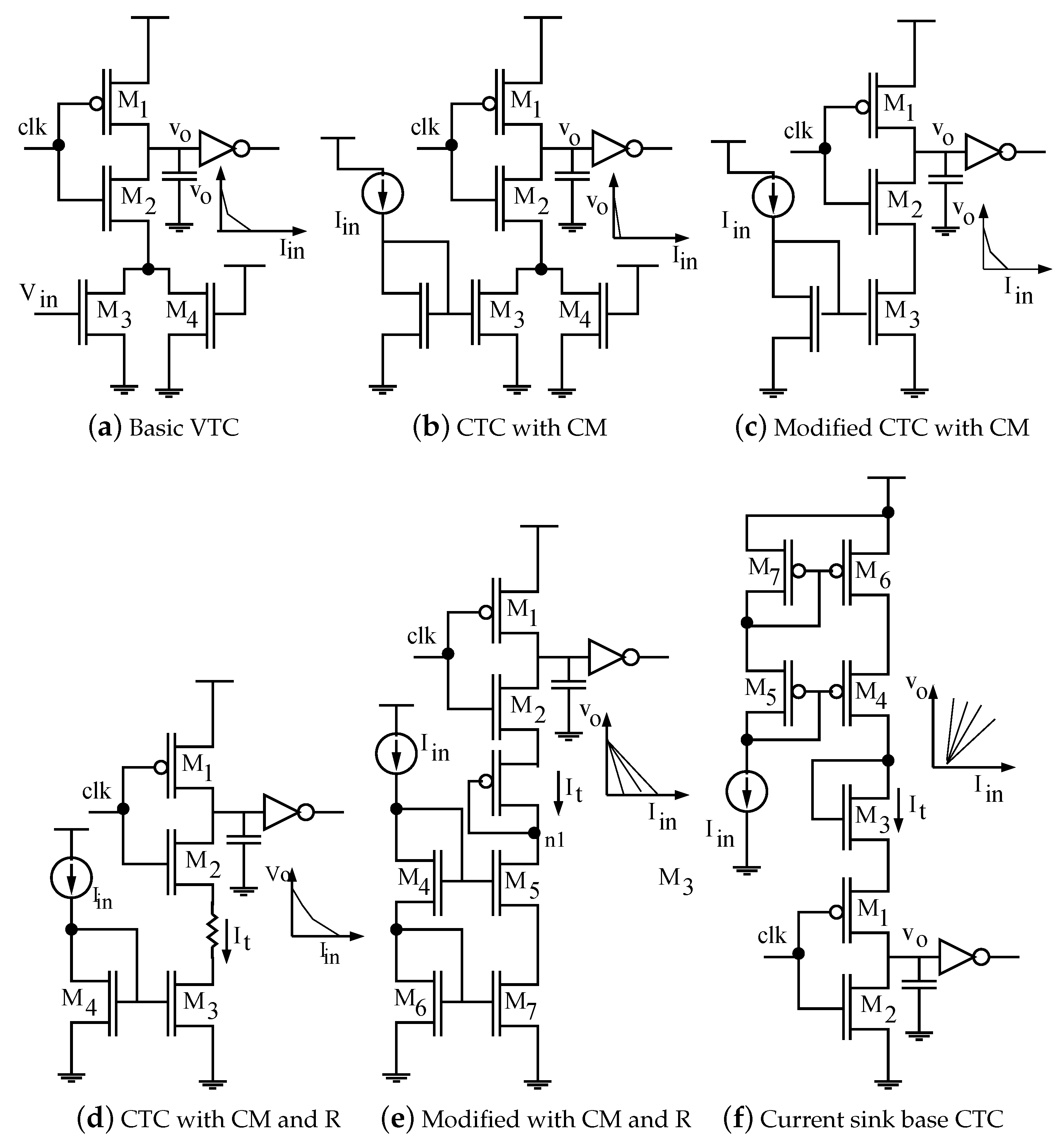
Figure 3 shows different CTC and VTC circuits and their transfer characteristics. The circuit in
Figure 3a is the basic structure of a VTC, which is based on a voltage-controlled delay unit (VCDU). At the falling edge of the controlling clock (
), the node capacitor (
) gets charged by
. The charging time of (
) can be controlled by the conductance of the PMOS (M1). During the rising edge of the clock (
), the node capacitor discharges through the transistors M2, M3, and M4. Since
controls the conductivity of the M3 transistor, it is used to control the discharge current of the node capacitor. Therefore, the rising time of the output voltage is controlled by
. Ideally, the rising time of the output voltage should linearly change with an input voltage of
. However, the transfer characteristics of the MOSFET are nonlinear following the square law. Therefore, developing the desired linear relationship cannot be possibly achieved using the circuit configuration in
Figure 3a.
Figure 3b shows a circuit configuration that provides a possible way to achieve such a linear relationship. In this configuration, a current mirror (CM) made up of two transistors is used to replace the M3 transistor in
Figure 3a. This makes the current flowing in M3 of
Figure 3b the same as the input mirror current (
). Due to the high impedance of the current mirror, the largest portion of the total current will flow through the M4 transistor and hence a very small conversion gain will be provided. Therefore, an improved design is shown in
Figure 3c, which is further modified in
Figure 3d. An additional resistance R has been used to generate a linear current source, which is necessary to maintain the M3 transistor in the saturation region. This will emphasize the linearity of the output delay. However, including such a resistance requires a challenging fabrication process. Therefore, the resistor has been replaced by a diode-connected active current source as shown in
Figure 3e. The circuit configuration in
Figure 3e also includes a cascaded current mirror that is needed to achieve maximum conversion gain. A PMOS-based circuit also can be designed using the same technique as shown in
Figure 3f.
3. Small Signal Model and Simulation Results
Figure 4a shows the small-signal equivalent circuit diagrams of the proposed CTC. The output capacitor (
) charges and discharges at the rising and falling edges of the control clock (
), respectively. As mentioned earlier, the discharging time is important for the proposed CTC because we are controlling the rise time of the CTC. A model for the discharging time is shown as follows:
where
,
, and
are the trans-conductance of the M1, M3, and M5 transistors, respectively.
is the y-intercept of line as shown in
Figure 5. Now conductance can also be given as the slope of the curve as shown in the
Figure 5. The delay behavior of the output for the proposed CTC is modeled as:
The linear relationship between input current (
) and output voltage (
) very much depends on the resistance value of the diode-connected M3 transistor, which is shown in
Figure 6 (this is a simulation result). M3 is working as a biasing current source for the cascaded current source, which is the next unit for the proposed CTC. In
Figure 6, curves become straighter with the increase in device length because MOSFET resistance increases with the increment in channel length. In
Figure 6, the high value of resistance of the M3 transistor helps to increase linearity because the long channel device limits the second-order and nonlinear effects such as short channel, subthreshold, channel length modulation, and gate-induced drain leakage (GIDL). Linearity is also dependent on the width of the M3 transistor, because it is inversely proportional to resistance, which is shown in
Figure 7. A wide width transistor also reduces the nonlinearity in the drain current due to the short channel effect. In
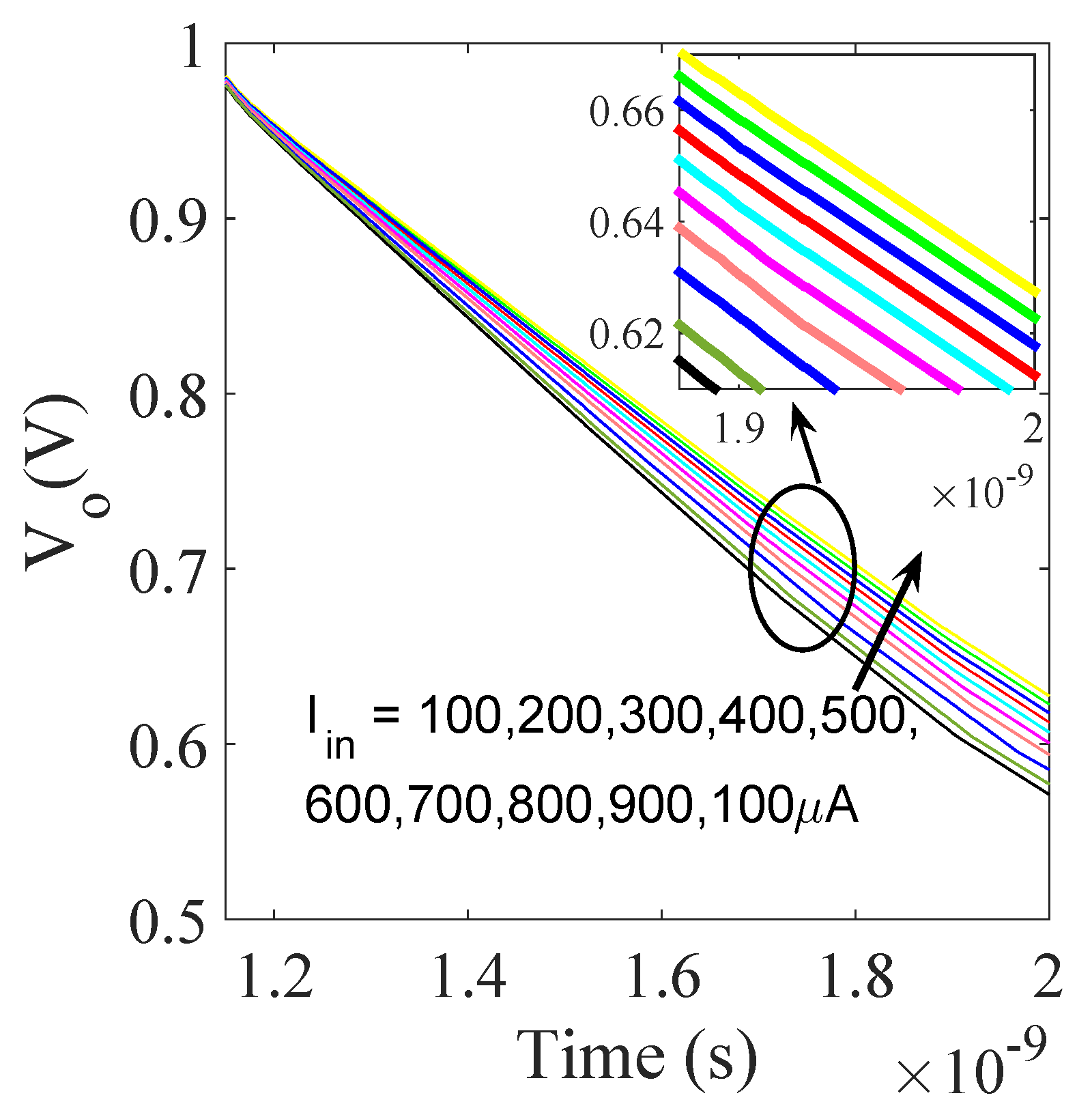
Figure 3e, as per the working principle, the current mirror copies the input current on the output node (n1). Further, the cascaded current mirror reduces the channel length modulation and increases output resistance. It also reduces the errors in output currents because of the internal property of the current mirror. The discussed modification in the proposed CTC makes it more efficient than the state-of-the-art designs. The simulation results of the proposed CTC are shown in
Figure 8. Simulation results show the linear change in the
node voltage for different input currents. The step size in the output is almost symmetric with the symmetric change in the input current, because the strong M3 transistor biases the cascaded current mirror and the cascaded state also provides extra linearity. The proposed work is part of the ADC and the conversion gain is the main parameter for us. We tried to increase the conversion gain. The detailed comparison of the conversion gain with the state-of-the-art experimental result is shown in
Table 1 [
15,
22]. The characteristics of the proposed CTC are shown in
Figure 5. The conversion gain of the proposed CTC is 3.86 ms/A, which is 52 times larger than the state-of-the-art design [
15]. The robustness of the proposed design is discussed in the following section.
4. Robustness Analysis
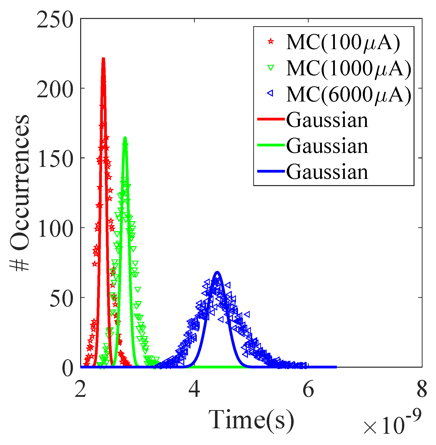
We have used the current mirror circuit in order to design the CTC, which is sensitive towards the MOSFET device parametric variation due to the process, temperature, and supply voltage variations. We used only four transistors for the current mirror circuit, which is not a large area penalty, and hence we can increase the sizing of this transistor. To check the robustness of the proposed CTC circuit, we analyzed the effects of nonidealities on the output delay. We have considered nonidealities in the W, L, and threshold voltage variation of the MOSFET. We have assumed a 10% global variation in the threshold voltage. We have used 5000 Monte Carlo (MC) simulations at a six sigma deviation for the process variation analysis.
Figure 9 shows the simulation results for
A,
A, and
A input currents. The results show very little deviation (
) from the mean value, which means that the design is stable and robust. We have chosen these values because the built-in computational random access (C-RAM) with 64 columns and all store data in high logic produces a maximum
A current. Hence, ADC can be used in built-in C-RAM designed using the proposed CTC. C-RAM is the important block of the CNN accelerators that is used in an autonomous vehicle.
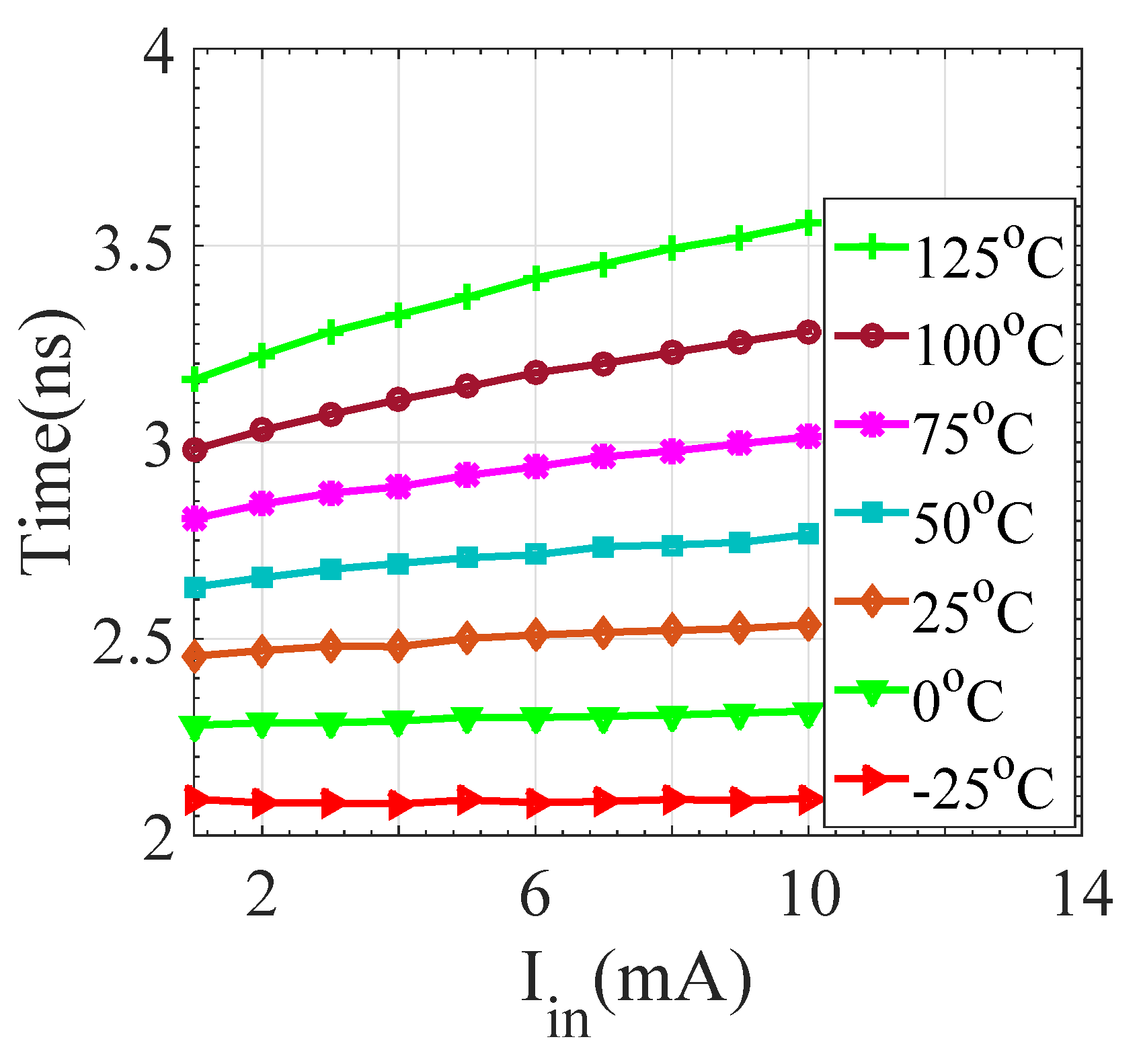
Output delay with temperature variation is shown in
Figure 10. The simulation results show the sensitivity with temperature variation. Results show that the CTC is very much sensitive to temperature variation. Hence, the specifications, i.e., the initial conditions of the CTC, will change with temperature. However, it is showing a linear shift in delay with temperature; thus, it can be repaired. Further,
Figure 11 shows the change in output delay with a 10% variation in supply voltage, and results show a minimal difference. Hence the circuit can tolerate the supply voltage variations.
We next tested the reliability of the proposed CTC using the Mosera Model. The performance of the CTC decreases due to the reliability degradation sources such as NBTI and PBTI. The increment in the threshold voltage of the P-type MOSFET due to NBTI is due to the diffusion of hydrogen ions into the gate oxide. It gets accelerated under the electric filed due to direct current (DC) and alternating current (AC). The shift in threshold voltage due to DC stress is given by:
where
is approximately
,
is the hydrogen generation constant,
is the annealing constant,
is the initial trap charge density, and
is the hydrogen diffusion constant.
n depends on the different device sizes and material parameters.
n is ≈0.25 for the FinFET and MOSFET devices. The shift in threshold voltage due to AC stress is given by:
where
is the technology-dependent parameter and it is equal to the
. The
is a prefactor, and the value of the prefactor depends on the operating frequency and the gate input probability (
). Moreover, it is reported that the lifetime is four times larger in AC than in DC stress. In the state-of-the-art design, charging and discharging of the output capacitors is done by PMOS [
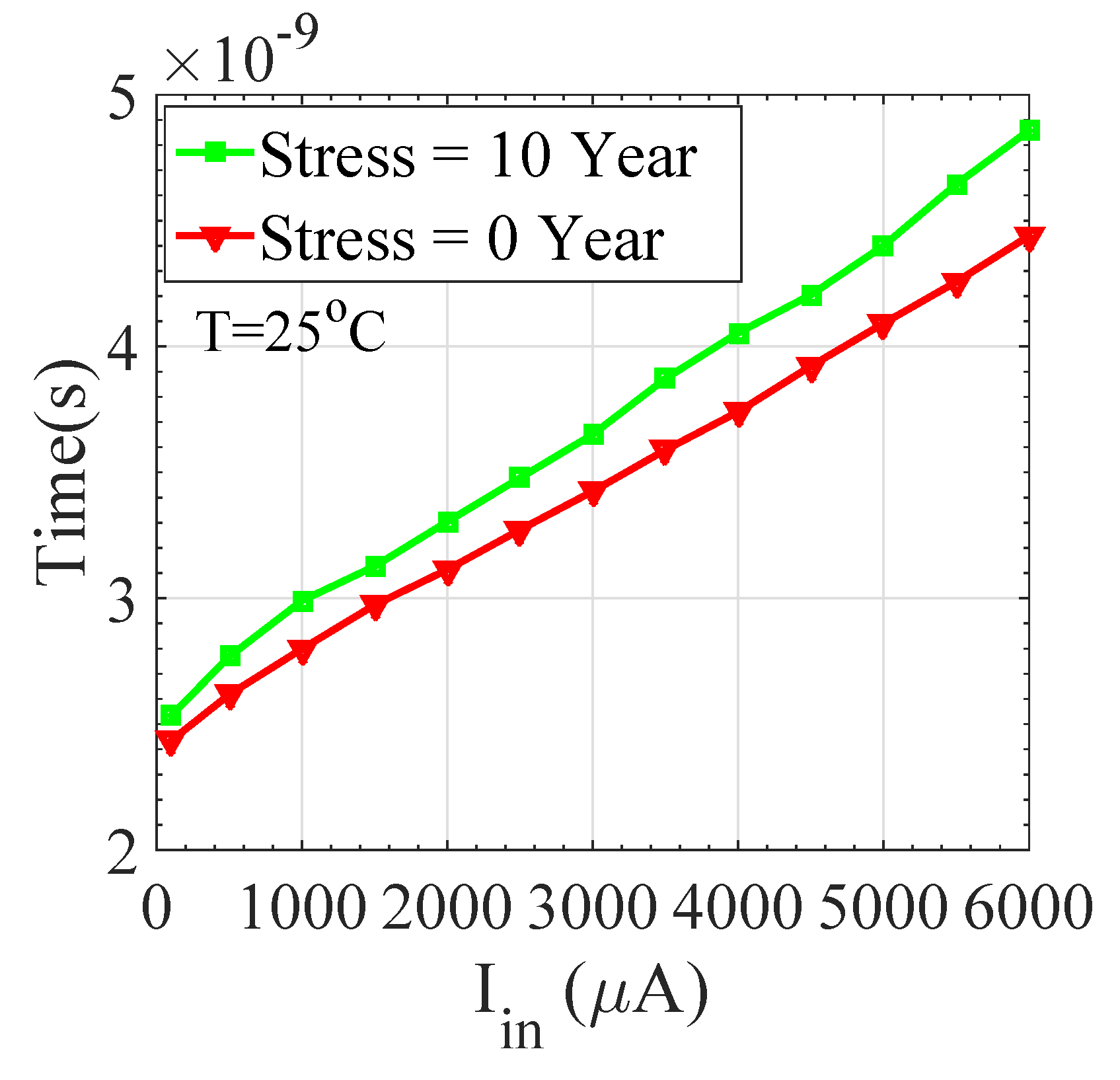
15]. From the literature, NBTI is the major reliability source that increases the threshold voltage of the PMOS transistors. Hence, we can conclude that state-of-the-art designs are not reliable. The simulation results for reliability due to NBTI and hot carrier injection (HCI) are compared in
Figure 12. The figure compares the voltage-to-time characteristics for ten-year DC stress. The proposed circuit shows a maximum 8.6% shift in results for ten-year stress, which is much smaller than the most advanced available state-of-the-art designs [
15].
5. Time-To-Digital Conversion
The CTC provides the time interval for the input current; it next needs a device that can provide digital data. We need a time-to-digital converter circuit for the digital output. TDC is also known as a data converter, i.e., it moves between different number domains. TDC is accountable for converting a time interval into a digital coded number. The TDC can be designed with various methods such as single counter, Flash TDC, vernier oscillator and a cyclic pulse-shrinking-based vernier-oscillator.
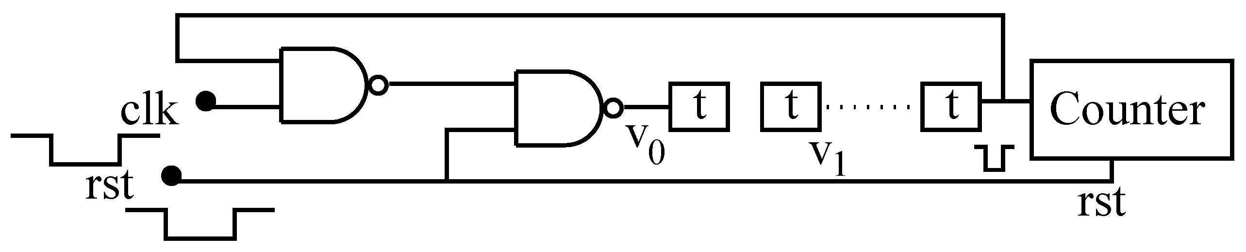
The single counter is the simplest type of TDC, which is shown in
Figure 13 [
23]. This TDC counts clock pulses for the time interval between rising edges of the start and stop signals. The clock frequency of the counter is higher than the clock frequency of the CTC. Even though, the proposed circuit provides a 15 ps delay for every
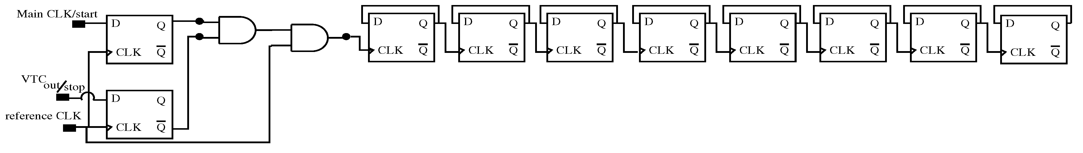
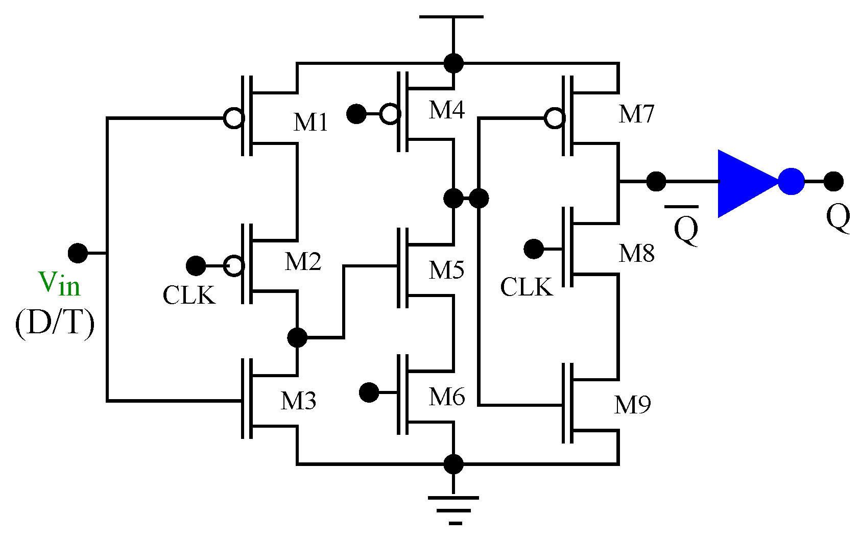
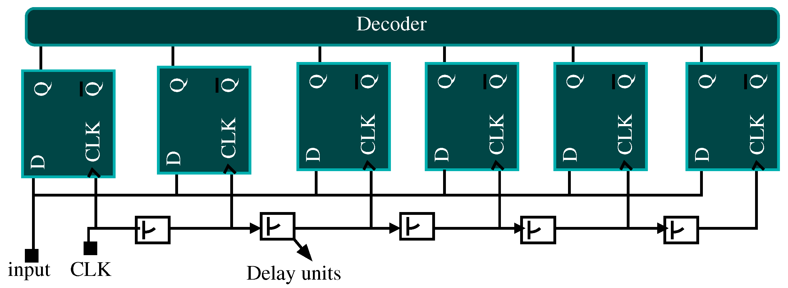
A input current, a 15 ps delay is not sufficient for conventional counter-based TDCs. Hence series-connected CTCs are used for the sufficient delay generation. First, we have designed a counter-based TDC using the best available T-flip-flop and the same is shown in
Figure 14 [
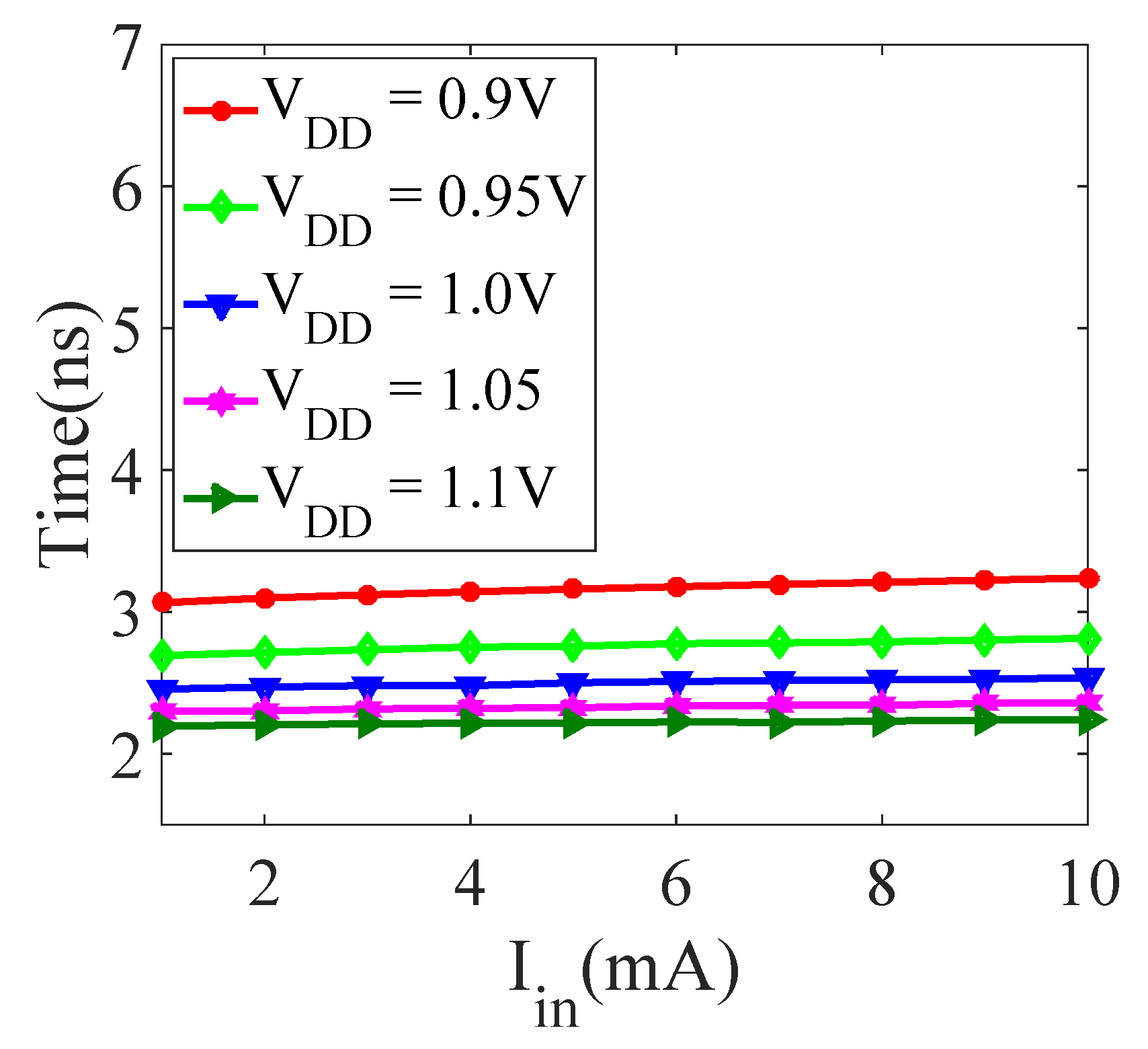
24]. This is a three-stage circuit and it uses nine transistors. The output characteristic of the designed clock frequency for 2 GHz is shown in
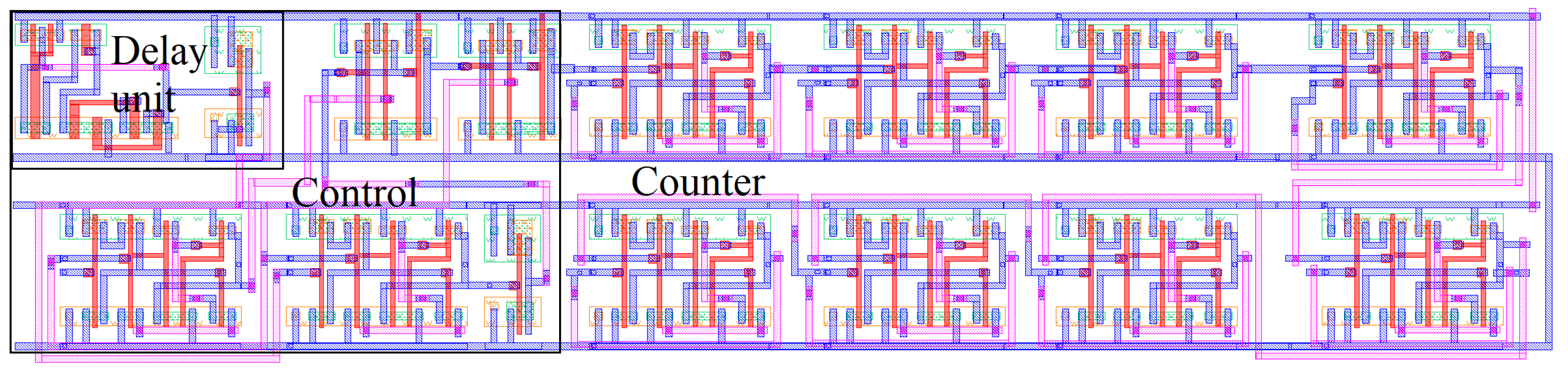
Figure 15. This counter can support a maximum of 4 Ghz frequency with a 60 pico-second rise and fall time. The resolution of this circuit depends on the frequency of the reference clock and can be no higher than a clock period. The counter-based TDC consists of delay units, control logic, and an 8-bit counter. The layout of the counter-based TDC is shown in
Figure 16. The dimensions of the layout are
m, which is much smaller than the best available state-of-the-art design [
15]. The exact area compression is not possible to define because the published result is on different technology nodes and hence we are using approximate information for the area comparison. However the very high frequency-based flip-flop design and the stability of the on-chip clocks limit this design.
Flash TDC is another type of data converter. The block diagram of the Flash TDC is shown in
Figure 17 [
18]. In this design, each delay unit generates a
delay. The chain of delay units produces an incremental delay and every output is
time. It is a very fast and efficient design but initial tuning of this design is difficult. Further, a Vernier delay line-based flash TDC is proposed to increase the resolution [
20]. This type of TDC is well suited for on-chip timing measurement on every clock cycle. A component-invariant Vernier oscillator TDC with a phase detector is proposed to generate the perfect square waves based on the very small input frequency. It uses two ring oscillators for the synchronization. It also uses the start and stop signals as the counter-based TDC was to enable the oscillators. The block diagram of the Vernier oscillator-based TDC is shown in
Figure 18 [
20]. The limitation of this architecture is that it takes many cycles to complete a single measurement. This why the Vernier oscillator requires a long conversion time.
Further, the pulse-shrinking-based TDC can be used to reduce the long conversion gain [
25]. It can also be further modified by the ring oscillator to quantize a time interval based on a very small frequency difference between the two oscillators. It is also further modified by the cyclic pulse-shrinking circuit, which is shown in
Figure 19 [
25]. It uses a delay line in the feedback loop to design a TDC. In
Figure 19, the counter counts the width of the input pulse. In this design, the delay unit can be designed by the chain of inverters and the counter counts the clock until the input pulse disappears.


