Abstract
In this paper, a frequency tunable planar balun composed of varactors loaded coupled lines (VL-CLs) is presented. By tuning the capacitances of the varactors, a wide frequency tuning range is obtained. Moreover, good impedance match, balanced output ports amplitude, and consistent output ports phase difference (PD) are maintained during the tuning. A detailed theoretical analysis using the signal flow diagram and the even-odd mode method is presented to clarify the characteristics of the proposed balun. To achieve ideal output matching and isolation for the proposed balun, a novel frequency tuned isolation circuit (IsC) is designed and connected to the balun. In theory, a frequency tuning range of 200% can be realized. In practice, due to the limited capacitances of the varactors, a prototype with a tunable frequency of 1.0 GHz ~ 2.0 GHz (66.7%) is designed, fabricated, and measured. The measured results show that more than21 dB of return loss (RL), 180° ± 1.8° of phase difference, 0.43 dB of amplitude imbalance (AP), and 22 dB of isolation are obtained at all tuning center frequencies, agreeing well with the simulated results.
1. Introduction
Balun [1,2], which transforms unbalanced signals into balanced signals, is an important component widely used in RF (radio frequency) circuits, such as frequency doubler [3], mixers [4], power amplifiers [5] and antenna feed networks [6]. In recent years, the planar baluns [7,8,9] have received extensive attention and research due to their compact structures and good performance. Among them, planar Marchand baluns are commonly investigated and used. In the past, modifications of the planar Marchand baluns have been reported, including bandwidth enhancement [10,11], miniaturization [12,13], and the design of an isolation circuit (IsC) [14,15]. However, two ports of the Marchand balun should be terminated to ground by using via-holes. This not only complicates the fabrication process, but also causes additional parasitic effects. Recently, a novel structure of planar balun [16] was proposed. Since it is based on trans-directional coupled lines, no via-holes are required and the inductive effect can be avoided.
With the development of wireless communication technology, the demands for reconfigurable components which could cover multiple bands are increasing. Thus, various frequency tunable front-end circuits have been developed, such as power dividers [17,18], couplers [19,20], and baluns [21,22,23,24]. In Reference [21], a compact frequency tunable microstrip balun with a ring structure is proposed. However, the return losses (RL) and the phase difference (PD) needed to be improved (RL < 18 dB at each tuning center frequency and PD in the range of 180° ± 7°). In Reference [22], a frequency tunable balun with bandpass response is proposed. It has a tunability of 51%. But the RL is deteriorated along with the frequency increases. Later, a bandwidth tunable filtering balun based on compact 3D configuration is presented [23]. It has a 34.3% frequency tuning range, and a wide bandwidth. However, high losses and poor PD are also exhibited. Moreover, since perfect port impedance match cannot be achieved by the reported structures [21,22,23] in each tuning center frequency, a narrow frequency tuning range is inevitable. In Reference [24], a differential coupling structure for tunable evanescent mode cavity resonators with a 62.4% frequency tuning range is reported. However, the RL is still worse (about 20 dB at all tuning center frequencies). Besides, an ideal output matching and isolation should be maintained for the frequency-tuned baluns in the entire tuning range. However, no IsC are provided in References [21,22,23,24].
In this paper, a frequency tunable planar balun with wide frequency tuning range is proposed. It is based on varactors loaded coupled lines (VL-CLs). By tuning the capacitance of the varactors, the operating frequency can be flexibly adjusted and perfect impedance match can be achieved at each tuning center frequency. As such, a novel frequency-tuned IsC is designed and connected to the proposed balun for achieving ideal isolation at the tuning states.
2. Theoretical Analysis
2.1. Design Equations for the Balun
Figure 1 shows the schematic of the proposed frequency tunable balun. It is composed of two identical VL-CLs with one port of the first VL-CL connected with the adjacent port of the second VL-CL. One of the VL-CL consists of three sections of coupled lines and three types of varactors. Two types of varactors, denoted as C1 and C2, are connected between the middle of each coupled line. Another type of varactor, denoted as C3, is connected between the center of the middle coupled line and the ground. The characteristic impedances of the even- and odd-mode coupled lines are represented by Z′0{e,o}. The electrical length of each coupled line is defined as θ′0 at the operating frequency f0. Z0 is the port impedance.
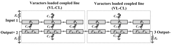
Figure 1.
Schematic of the proposed frequency tunable balun.
To simplify the analysis of the proposed structure, the VL-CLs in Figure 1 can be equivalent to parallel coupled lines (coupled line A and coupled line B), as shown in Figure 2. Let Z0{e,o} and θ{e,o} represent the equivalent even- and odd- mode characteristic impedances and electrical lengths, separately. Based on even-odd mode analysis [25], the S-parameters of the parallel coupled line (A or B) in Figure 2 can be described as:
where S11{e,o} and S21{e,o} are the even- and odd-mode S-parameters of the coupled line. By using transmission line analysis, we have
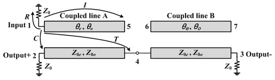
Figure 2.
Equivalent circuit of the proposed balun for signal flow analysis.
Signal flowcharts are used to derive the S-parameters of the proposed balun. For convenience, the SCoupled line,11, SCoupled line,51, SCoupled line,41, and SCoupled line,21 are replaced by R, I, T, and C, as shown in Figure 2. Figure 3 shows the signal flow analysis of the proposed balun at port 1. According to Figure 3, the S-parameters (S11, S21 and S31) of the balun at port 1 can be derived as shown in Equation (3). Detailed derivations are discussed in Appendix A.
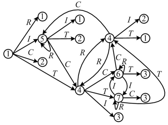
Figure 3.
Signal flow analysis of the proposed tunable balun at port 1.
To realize perfect impedance match, and balanced output amplitude, the following relations should be satisfied:
Firstly, by substituting Equations (1), (3b) and (3c) into Equation (4b), the following equation can be obtained:
Then, after solving Equation (5) with Equation (2), the even- and odd-mode equivalent electrical length θ{e,o} are derived:
Finally, the relations between Z0e and Z0o can be calculated when substituting Equations (1), (2), (3a) and (6) into Equation (4a):
It can be found from Equations (6) and (7) that perfect match and balanced output amplitude can be achieved if the values θ{e,o} are selected according to Equation (6) and the relations of Z0e and Z0o are fixed using Equation (7). When the equivalent even- and odd-mode characteristic impedances Z0{e,o} and the electrical lengths θ{e,o} are determined, the circuit parameters of the VL-CLs can be obtained. In the following, the relations of the circuit parameters between the VL-CLs and the equivalent parallel coupler lines (E-PCLs) are derived.
Firstly, the even- and odd-mode ABCD matrices of one E-PCL can be described as:
Secondly, the even- and odd-mode ABCD matrices of one VL-CL are analyzed. By multiplying the ABCD matrices of each cell (M′1{e,o}, M′2{e,o} and M′3{e,o}) in Figure 4, the overall ABCD matrix of the VL-CL can be obtained as shown in Equation (9).
where
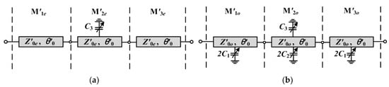
Figure 4.
(a) Even-mode schematic of the varactors loaded coupled line (VL-CL); (b) odd-mode schematic of the VL-CL.
It is noted that b1{e,o} represent the even- and odd- mode shunt susceptance of the first and third coupled lines, b2{e,o} represent the even- and odd- mode shunt susceptance of the second coupled line. If the shunt susceptances are implemented by C1, C2, and C3, we have
Thirdly, substituting Equations (6) and (7) into Equation (8), the following equations can be obtained:
Finally, since the ABCD matrices of Equation (8) is equal to the ABCD matrices of Equation (9), A{e,o}= A′{e,o}, B{e,o}= B′{e,o}, and C{e,o}= C′{e,o} are obtained. By substituting Equations (9) (10), and (11) into Equation (12), the mathematical expressions of C1, C2, and C3 can be computed as:
where L1, L2, L3, L4, L5, and L6 can be described as:
and N1, N2, N3, N4, N5, and N6 can be described as:
It is observed from Equations (13), (14), and (15) that the operating frequency f0 can be adjusted by changing C1, C2, and C3 when θ′0, Z′0e, and Z′0o (Z′0e and Z′0o can be assigned freely) are fixed. Since C3 should be larger than 0 pF, the value of θ′0 must be less than π/6, as indicated in Equation (13c). Thus, the relation between θ′0 and the operating frequency f0 is
where f1 is the maximum tuning frequency.
2.2. Isolation Circuit for the Balun
To achieve ideal output matching and isolation for the proposed balun, an IsC should be added between the output ports. According to the analysis of IsC in Reference [14], the design of IsC is determined depending on the output phase delays ( and ). If is assumed to be θB, should be θB ± 180°. Although the design method of IsC under different θB is analyzed, the influence of θB on the output matching and isolation is not given. According to the design method of IsC in Reference [14], the effect of θB on the output matching (|S22|) and isolation (|S23|) is simulated, as shown in Figure 5. The relative bandwidths for |S22| < − 20 dB and |S23| < − 20 dB are decreased with the decrease of θB. When θB reduced to 10°, the performance of IsC becomes very poor (the relative bandwidths for |S22| < − 20 dB and |S23| < − 20 dB are less than 0.8%). So the value of θB is important for the design of IsC. In order to get the value of θB for the proposed balun, the S-parameters needs to be known. When the input port of the proposed balun is perfectly matched, its S-parameters can be expressed according to the design equations in Section 2.1, as shown below.
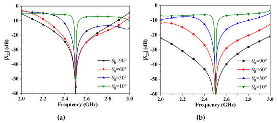
Figure 5.
The effect of θB on the performance of IsC. (a) |S22|; (b) |S23|.
The value of θB for the proposed balun is 0°, so the IsC cannot be directly connected to the proposed balun. Without affecting the performance of the proposed balun, two identical transmission lines are connected between the output ports of the balun and the IsC, as shown in Figure 6. The characteristic impedance and the electrical length of the transmission line are represented by Z0 and θR. When the output phase delay is increased by θR, the S-parameters matrice of the balun can be expressed as:
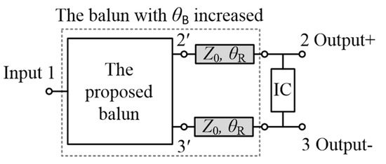
Figure 6.
Method for IsC connected to the proposed balun.
It can be found from Equation (18) that the value of θB is increased to θR, and perfect impedance match is maintained. In order to achieve ideal output matching and isolation, the value of θB is selected as λ/4 and the structure of IsC can be obtained from Reference [14]. It is noted that the electrical length of each transmission line should remain unchanged at the center frequency when the frequency is tuned. To satisfy this condition, transmission lines with variable electrical lengths [26] are used. Figure 7 shows the schematic of the designed frequency-tuned equivalent transmission line and IsC. The values of Z1e, Z1o, θ1, θ2, and L can be assigned according to the analysis in Reference [26]. By changing the values of C4 and C5, the electrical lengths of the original transmission lines can be tuned and perfect isolation can be achieved at each tuning center frequency.
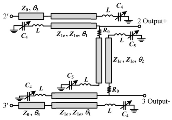
Figure 7.
The schematic of the equivalent transmission line and IsC.
2.3. Design Procedure
The design procedures of the proposed tunable balun with IsC are summarized as follows:
- Determine the maximum tuning frequency f1 as needed, and (θ′0)max is predefined as π/6 at the maximum tuning frequency f1.
- The value of θ′0 can be calculated by Equation (16), and the values of Z′0e and Z′0o can be assigned freely according to fabrication limitation of a real coupled line.
- C1, C2 and C3 can be computed from Equations (13)–(15) under the required operating frequency f0 with known θ′0, Z′0e, and Z′0o.
- The values of Z1e, Z1o, θ1, θ2, and L can be assigned according to the tuning range of the electrical length from Reference [26].
- C4 and C5 can be computed from Reference [26] under the required operating frequency f0.
- With the obtained parameters, the circuit can be optimized using the Advanced Design System (ADS).
In the following, a prototype is designed and fabricated to validate the proposed structure.
3. Experimental Results
In this section, a frequency tunable balun with a maximum tuning center frequency (f1) of 2.5 GHz is designed. C1, C2, and C3 are functions of the operating frequency f0 when other circuit parameters are fixed, as observed in Equation (13). The curves of C1, C2, and C3 versus the tuning frequency (f0) are plotted, as shown in Figure 8. Here, Z′0e and Z′0o are chosen as 120.7 Ω and 77.3 Ω according to fabrication limitation of a real coupled line. It is found that the capacitances C1, C2, and C3 both increase with the decrease of f0. Under the criterion of C1 > 0, C2 > 0, and C3 > 0, the theory frequency tuning range is about 200%. Also using Figure 8, the suitable values of C1, C2, and C3 for each tuning frequency can be calculated directly and accurately, which is simple and is a timesaver. Z1e, Z1o and L of the proposed IsC are chosen as 126.8 Ω, 19.2 Ω and 2.2 nH according to the analysis in Reference [26]. Based on the tuning range and the realization values of varactors, θ1 = θ2 = 150° at the frequency f1 are chosen to achieve a tunable phase delay of θR. In order to achieve a phase delay of 90° (270°), transmission lines with Z0 = 50 Ω and θ3 = 90° at the frequency f1 are needed to be connected to the IsC.
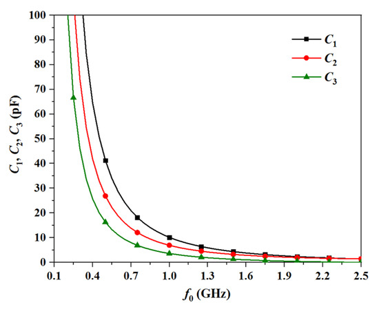
Figure 8.
Curves of C1, C2, and C3 versus the tuning frequency f0.
To demonstrate the validity of the aforementioned design theory and approach, an experimental prototype is simulated with ADS and fabricated using the F4–B substrate with a relative permittivity of 3.5, a loss tangent of 0.003, and a thickness of 1.5 mm.
3.1. Simulation Results
In this design, the frequency tuning range is chosen from 1.0 GHz to 2.0 GHz. The practical tuning range is deteriorated by the capacitance limitation of the varactors and the phase shift tuning range limitation of IsC. The design parameters of the prototype can be obtained according to the previous analysis. Based on the parameters, a prototype of the proposed balun with IsC was simulated with the ADS, and the simulated results are shown in Figure 9. To illustrate, several tuning center frequencies (1.0, 1.3, 1.7, and 2.0 GHz) are chosen as examples. The corresponding values of C1, C2, C3, C4, and C5 are listed in Table 1. It is observed from Figure 9 that a continuously frequency tuning range of 66.7% (1.0 GHz ~ 2.0 GHz) is obtained with a perfect return loss (|S11| < − 40 dB), equal output ports amplitude (|S21| = |S31| = − 3 dB), and consistent phase difference (∠S21 − ∠S31 = 180°) at each tuning center frequency. It is also recognized that ideal output matching and isolation can be obtained (|S22| < − 40 dB, |S33| < − 40 dB and |S23| < − 40 dB) at each tuning center frequency. Therefore, the theoretical analysis and approach described in Section 2 are confirmed to be correct and effective.
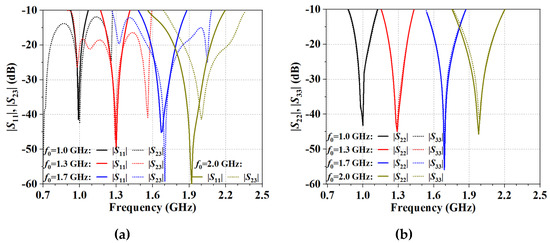
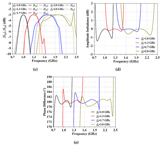
Figure 9.
Simulated results at 1.0, 1.3, 1.7, and 2.0 GHz. (a) |S11| and |S23|; (b) |S22| and |S33|; (c) |S21| and |S31|; (d) Amplitude imbalance; (e) Phase difference.

Table 1.
Capacitance of the varactors for different frequencies.
3.2. Measurement Results
Figure 10 shows the layout and photograph of the fabricated prototype. The overall dimension of the prototype is 61 mm × 71 mm. Values of components and the main optimized dimensions of the proposed tunable balun are shown in Table 2. Bias-voltage network consists of current limiting resistances Rbias and bypass capacitors Cbias for establishing proper biasing conditions for varactors. According to the capacitance range of varactors C1, C2, C3, C4, and C5 displayed in Table 1, the SMV1763 [27] is utilized for C1 and C2, the SMV2020 [28] is utilized for C3 and C5, and the SMV1265 [29] is utilized for C4 from Sky-works Solutions, Inc.. The capacitances of the varactors C1, C2, C3, C4, and C5 are controlled by V1bias, V2bias, V3bias, V4bias and V5bias. The dc blocking capacitors Cblock are applied to isolate dc voltages. The ground slot and patch at the ground layer are used to realize the high impedance ratio of the coupled lines for the single-layer PCB structure [30].
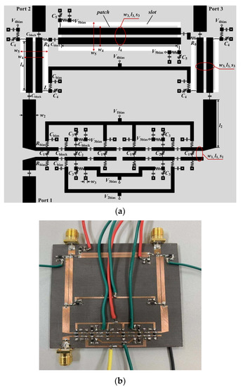
Figure 10.
(a) Layout and (b) photograph of the fabricated prototype.
Table 2.
Values of components and the main optimized dimensions of the prototype.
By using an Agilent N5230A microwave network analyzer, the measured results of the S-parameters, phase difference, and amplitude imbalance (AP) are obtained, as shown in Figure 11. It is observed that the prototype can be tuned from 1.0 GHz to 2.0 GHz (66.7%) continuously. During the tuning, the insertion losses are in the range of 4.0 − 4.7 dB and the return losses are more than 21 dB at each tuning center frequency. The output ports phase difference deviates from 0.3° to 1.8°. Moreover, great output matching (|S22| < − 22 dB, |S33| < − 22 dB) and isolation (|S23| < − 25 dB) are obtained at each tuning center frequency. Table 3 illustrates the values of V1bias, V2bias, V3bias, V4bias, and V5bias corresponding to the center frequencies of 1.0, 1.3, 1.7, and 2.0 GHz, and Table 4 illustrates the detailed relative bandwidth of the fabricated tunable balun. At the tuning center frequencies, the relative bandwidth for |S11| < − 10 dB is more than 20.0%, while the relative bandwidths for AP < 1.5 dB and PD = 180° ± 4° are greater than 32.0% and 35.0%, respectively. The relative bandwidths are decreased along with the tuning center frequency decreases. The main reason for the narrow bandwidth is the nonlinear relationship between the capacitances and the tuning center frequency, as shown in Figure 8. It is observed that the values of the capacitors change more sharply at the lower frequency bands than at the higher frequency bands.
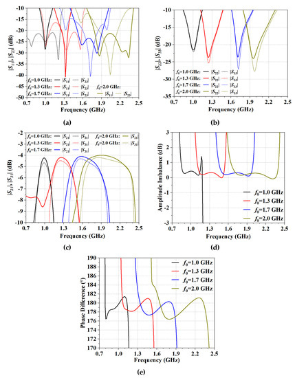
Figure 11.
Measured results at 1.0, 1.3, 1.7, and 2.0 GHz. (a) |S11| and |S23|; (b) |S22| and |S33|; (c) |S21| and |S31|; (d) Amplitude imbalance; (e) Phase difference.
Table 3.
The values of V1bias, V2bias, V3bias, V4bias, and V5bias for different frequencies.
Table 4.
Relative bandwidth of the fabricated tunable balun.
Figure 12 shows the measured input third-order intercept point (IIP3) versus the tuning center frequency. It is observed that the IIP3 increases along with the frequency increases. When the frequency varies from 1.0 GHz to 2.0 GHz, the IIP3 are in the range of 25.8 dBm – 33.2 dBm. To investigate the power handling of the proposed structure, the |S21| at 1.0 GHz and 2.0 GHz are measured with different input powers, as shown in Figure 13. It is seen that the losses are increased with the increasing of the input power, and the power handling of the circuit is increased along with the frequency increases. It can be estimated that during the tuning from 1.0 GHz to 2.0 GHz, the power handling of the proposed balun is 8 dBm.
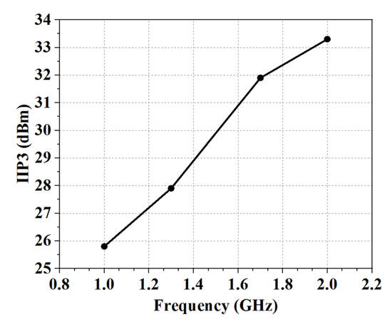
Figure 12.
Measured IIP3 versus frequency.
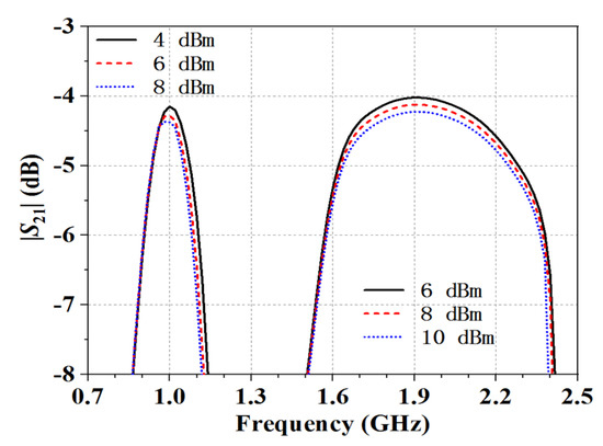
Figure 13.
Measured |S21| for different input powers at 1.0 GHz and 2.0 GHz.
4. Discussion
Table 5 summarizes the comparisons between the proposed balun and other frequency tunable balun that can be found in the literature. Perfect port impedance match at each center frequency cannot be achieved in References [21,22,23], while this feature can be achieved by the proposed balun. It is exhibited from Table 5 that the performances of the proposed balun exceed the performances of the former ones [21,22,23] in terms of the return loss, insertion loss, amplitude imbalance, phase balance, and tunability. Although the amplitude imbalance and phase balance of the balun in Reference [24] are slightly better than that of the proposed balun, the return loss and tunability of the balun in Reference [24] are still needed to be improved. Moreover, frequency-tuned IsC is proposed in this design for the tunable balun, while no IsC is introduced in References [21,22,23,24]. In summary, the designed balun exhibits superior performances and is suitable for RF circuits.
Table 5.
Comparisons between the proposed tunable balun and the reported ones in literature.
5. Conclusions
The paper presents a frequency-tuned planar balun using VL-CLs. Detailed formulations are derived using the signal flowchart and the even-odd mode analysis. Design procedures are also given. To achieve ideal output matching and isolation for the proposed balun, a novel frequency-tuned IsC is also designed. For demonstration, an experimental prototype was designed, fabricated, and measured. The measured results show that the proposed balun can be tuned from 1.0 GHz to 2.0 GHz (66.7%) with good return losses, less insertion losses, balanced output ports amplitude, and consistent phase difference. Compared with the former frequency-tuned baluns, the proposed balun exhibits superior performances.
Author Contributions
S.F., X.G. and H.L. contributed to the overall study design, analysis, and writing of the manuscript. Z.W. provided technical support and revised the manuscript. All authors have read and agreed to the published version of the manuscript.
Funding
This work was supported in part by the National Natural Science Foundation of China under Grant 51809030 and Grant 61871417, in part by the China Post-Doctoral Science Foundation under Grant 2017M611210, and in part by the Innovation Project of Dalian Maritime University under Grant CXXM2019SS008.
Conflicts of Interest
The authors declare no conflict of interest.
Appendix A
In order to derive the S-parameters of the proposed balun easily, the signal flow diagram in Figure 3 can be divided into three parts as shown in Figure A1.
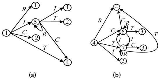
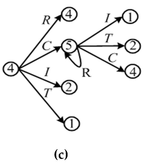
Figure A1.
(a) The signal is input from port 1 to coupled line A; (b) The signal is input from port 4 to coupled line B; (c) The signal is input from port 4 to coupled line A.
Figure A1a shows when a signal is input from port 1 to coupled line A, it is finally output from port 1, 2 and 4. Thus, the corresponding S-parameters can be represented by R1, C1 and T1 as follows
Figure A1b shows when a signal is input from port 4 to coupled line B, it is finally output from port 3 and 4. Thus, the corresponding S-parameters can be represented by I2 and R2 as follows
Figure A1c shows when a signal is input from port 4 to coupled line A, it is finally output from port 1, 2 and 4. Thus, the corresponding S-parameters can be represented by T3, I3 and R3 as follows
The signal flow diagram in Figure 3 can be equivalent to the signal flow diagram shown in Figure A2. Thus, the SBalun,11, SBalun,21 and SBalun,31 can be expressed by R1, C1, T1, I2, R2, T3, I3 and R3 as follows
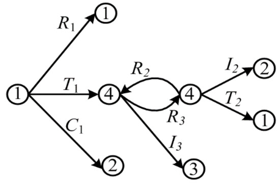
Figure A2.
The equivalent signal flow diagram of the proposed tunable balun.
By substituting Equations (A1), (A2) and (A3) into Equation (A4) and simplifying it, the expression of Equation (3) are obtained.
References
- Ang, K.S.; Robertson, I.D. Analysis and design of impedance-transforming planar Marchand baluns. IEEE Trans. Microw. Theory Technol. 2001, 49, 402–406. [Google Scholar]
- Zhang, W.; Wu, Y.; Liu, Y.; Yu, C.; Chen, W. Compact coupled-line balun with complex impedances transformation and high isolation. IET Microw. Antennas Propag. 2015, 9, 1587–1594. [Google Scholar] [CrossRef]
- Ye, Y.; Yu, B.; Tang, A.; Drouin, B.; Gu, Q.J. A high efficiency e-band CMOS frequency doubler with a compensated transformer-based balun for matching enhancement. IEEE Microw. Wirel. Compon. Lett. 2016, 26, 40–42. [Google Scholar] [CrossRef]
- Jeong, J.; Yom, I.; Yeom, K. An active IF balun for a doubly balanced resistive mixer. IEEE Microw. Wirel. Compon. Lett. 2009, 19, 224–226. [Google Scholar] [CrossRef]
- Smith, R.M.; Lees, J.; Tasker, P.J.; Benedikt, J.; Cripps, S.C. A novel formulation for high efficiency modes in push-pull power amplifiers using transmission line baluns. IEEE Microw. Wirel. Compon. Lett. 2012, 22, 257–259. [Google Scholar] [CrossRef]
- Deng, C.; Li, Y.; Zhang, Z.; Feng, Z. A wideband high-isolated dual-polarized patch antenna using two different balun feedings. IEEE Antennas Wirel. Propag. Lett. 2014, 13, 1617–1619. [Google Scholar] [CrossRef]
- Cho, C.; Gupta, K.C. A new design procedure for single-layer and two-layer three-line baluns. IEEE Trans. Microw. Theory Technol. 1998, 46, 2514–2519. [Google Scholar]
- Wang, J.; Huang, F.; Zhu, L.; Cai, C.; Wu, W. Study of a new planar-type balun topology for application in the design of balun bandpass filters. IEEE Trans. Microw. Theory Technol. 2016, 64, 2824–2832. [Google Scholar] [CrossRef]
- Zhang, Z.; Wu, K. A broadband substrate integrated waveguide (SIW) planar balun. IEEE Microw. Wirel. Compon. Lett. 2007, 17, 843–845. [Google Scholar] [CrossRef]
- Lin, K.; Lin, Y. A simple printed compensated balun for enhanced ultra-wideband performances. IEEE Microw. Wirel. Compon. Lett. 2014, 24, 5–7. [Google Scholar] [CrossRef]
- Lu, J.; Lin, C.; Chang, C. Exact synthesis and implementation of new high-order wideband Marchand baluns. IEEE Trans. Microw. Theory Technol. 2011, 59, 80–86. [Google Scholar] [CrossRef]
- Fathelbab, W.M.; Steer, M.B. New classes of miniaturized planar Marchand baluns. IEEE Trans. Microw. Theory Technol. 2005, 53, 1211–1220. [Google Scholar] [CrossRef]
- Shie, C.; Pan, Y.; Chin, K.; Chiang, Y. A miniaturized microstrip balun constructed with two λ/8 coupled lines and a redundant line. IEEE Microw. Wirel. Compon. Lett. 2010, 20, 663–665. [Google Scholar] [CrossRef]
- Ahn, H.; Itoh, T. New isolation circuits of compact impedance-transforming 3-dB baluns for theoretically perfect isolation and matching. IEEE Trans. Microw. Theory Technol. 2010, 58, 3892–3902. [Google Scholar] [CrossRef]
- Ahn, H.; Nam, S. New design formulas for Impedance-transforming 3-dB Marchand baluns. IEEE Trans. Microw. Theory Technol. 2011, 59, 2816–2823. [Google Scholar] [CrossRef]
- Shie, C.I.; Cheng, J.C.; Chou, S.C.; Chiang, Y.C. Design of a new type planar balun by using trans-directional couplers. IEEE Trans. Microw. Theory Technol. 2012, 60, 471–476. [Google Scholar] [CrossRef]
- Tang, W.; Ryu, J.H.; Kim, H. Compact, tunable Wilkinson power divider using tunable synthetic transmission line. Microw. Opt. Technol. Lett. 2010, 52, 1434–1436. [Google Scholar] [CrossRef]
- Shen, X.; Liu, Y.; Zhou, S.; Wu, Y. A novel compact tunable coupled-line power divider using varactors. In Proceedings of the Asia-Pacific Microwave Conference, Nanjing, China, 6–9 December 2015. [Google Scholar]
- Ferrero, F.; Luxey, C.; Staraj, R.; Jacquemod, G.; Fusco, V.F. Compact quasi-lumped hybrid coupler tunable over large frequency band. Electron. Lett. 2007, 43, 1030–1031. [Google Scholar] [CrossRef]
- Liu, H.; Fang, S.; Wang, Z. A compact trans-directional coupler with wide frequency tuning range and superior performance. IEEE Trans. Compon. Packag. Manuf. Technol. 2017, 7, 1670–1677. [Google Scholar] [CrossRef]
- Miao, X.; Zhang, W.; Geng, Y.; Chen, X.; Ma, R.; Gao, J. Design of compact frequency-tuned microstrip balun. IEEE Antennas Wirel. Propag. Lett. 2010, 9, 686–688. [Google Scholar] [CrossRef]
- Zhou, L.H.; Tang, H.; Chen, J.X.; Bao, Z.H. Tunable filtering balun with enhanced stopband rejection. Electron. Lett. 2012, 48, 845–847. [Google Scholar] [CrossRef]
- Yao, L.; Wu, Y.; Li, M.; Wang, W.; Liu, Y. Bandwidth-tunable filtering balun based on compact 3D configuration. Electron. Lett. 2019, 55, 32–34. [Google Scholar] [CrossRef]
- Hickle, M.D.; Peroulis, D. A widely-tunable substrate-integrated balun filter. In Proceedings of the 2017 IEEE MTT-S International Microwave Symposium, Honololu, HI, USA, 7–9 December 2017. [Google Scholar]
- Pozar, D.M. Microwave Engineering, 2rd ed.; John Wiley & Sons, Inc.: Hoboken, NJ, USA, 1998. [Google Scholar]
- An, B.; Chaudhary, G.; Jeong, Y. Wideband tunable phase shifter with low in-band phase deviation using coupled line. IEEE Microw. Wirel. Compon. Lett. 2018, 28, 678–680. [Google Scholar] [CrossRef]
- Data Sheet-SMV1763 Series Hyperabrupt Junction Tuning Varactors. Available online: https://www.semiee.com/file/EOL/Skyworks%20Solutions-SMV1763.pdf (accessed on 27 February 2020).
- Data Sheet-SMV2020 Series Hyperabrupt Junction Tuning Varactors. Available online: https://www.skyworksinc.com/en/Products/Diodes/SMV2020-079LF (accessed on 27 February 2020).
- Data Sheet-SMV1265 Series Hyperabrupt Junction Tuning Varactors. Available online: https://www.cdiweb.com/datasheets/skyworks/200063d.pdf (accessed on 27 February 2020).
- Abbosh, A.M. Analytical closed-form solutions for different configurations of parallel-coupled microstrip lines. IET Microw. Antennas Propag. 2009, 3, 137–147. [Google Scholar] [CrossRef]
© 2020 by the authors. Licensee MDPI, Basel, Switzerland. This article is an open access article distributed under the terms and conditions of the Creative Commons Attribution (CC BY) license (http://creativecommons.org/licenses/by/4.0/).