Article

Fault Diagnosis of Open-Switch Failure in a Grid-Connected Three-Level Si/SiC Hybrid ANPC Inverter

1
E&A Business Group, LSIS Co. Ltd., LS Tower, LS-ro 127, Dongan-gu, Anyang 14119, Korea
2
Department of Electrical and Computer Engineering, Ajou University, World cup-ro 206, Yeongtong-gu, Suwon 16499, Korea
*
Author to whom correspondence should be addressed.
Electronics 2020, 9(3), 399; https://doi.org/10.3390/electronics9030399
Submission received: 5 February 2020 / Revised: 25 February 2020 / Accepted: 27 February 2020 / Published: 28 February 2020
(This article belongs to the Special Issue High Power Electric Traction Systems)

Abstract

:
A diagnostic method for an open-circuit switch failure in a hybrid active neutral-point clamped (HANPC) inverter is proposed in this paper. The switching leg of the HANPC inverter consists of four silicon insulated gate bipolar transistors and two silicon carbide metal-oxide-semiconductor field-effect transistors to achieve higher efficiency and power density compared to conventional neutral-point clamped inverters. When an open-circuit failure occurs in a switching device, the output current is severely distorted, causing damage to the inverter and the connected loads. The proposed diagnostic method aims to detect the open-switch failure and protect the related devices without additional sensors or circuits. The faulty conditions of six different switches are investigated based on the current distortion in the stationary reference frame. By analyzing the individual characteristic of each switch failure, it is possible to detect the exact location of the failed switch in a short period. The effectiveness and feasibility of the proposed fault-diagnostic method are verified using simulation and experimental results.

1. Introduction

With increasing industrial energy loads and distributed generation systems, battery energy storage systems (BESSs) are widely adopted to limit the peak electric power demand and stabilize the power grid [1]. The BESS stores electricity from renewable energy resources or the grid to lithium secondary battery packs and provides energy to homes or businesses [2]. Energy management using the BESS reduces the needs for the entire generation capacity and gives flexibility in power distribution. As shown in Figure 1, the BESS consists of three major parts: the energy management system (EMS), the power conditioning system (PCS), and the battery. The PCS carries out the power conversion between the grid-side alternative current (AC) and the battery-side direct current (DC). Additionally, the PCS controls the direction of power flow from the grid to the battery or vice versa based on demand. A bidirectional power converter circuit is thus necessary to construct the PCS of the BESS. Three-level (3L) neutral-point clamped (NPC) inverters are suitable for the medium-power BESS [3].
The 3L-NPC inverter is a voltage source inverter (VSI) and produces three different output voltage levels depending on its switching states. The standard 3L-NPC inverter is composed of four silicon-based insulated-gate bipolar transistors (Si-IGBTs) and two clamping diodes in a leg. Four Si-IGBTs are connected in series and two clamping diodes are used to generate the neutral-switching state which connects the neutral-point of DC-link capacitors with the output terminal. For the medium-power PCS, however, the standard NPC inverter is used and has a limitation in terms of power density as it applies Si-IGBTs. Generally, a standard NPC inverter adopts low-switching frequency to reduce power losses and requires huge filter reactors to achieve a high quality of output currents. Additionally, the commutation loop of the standard NPC inverter differs between positive and negative directions of power flows. This implies that the loss profile of each switching device is not the same in the positive and negative power flows.
The three-level hybrid active NPC (3L-HANPC) inverter was introduced to get better efficiency and achieve a uniform power-loss profile in both power-flow directions [4]. The 3L-HANPC is composed of six switching devices, four Si-IGBTs, and two silicon carbide metal-oxide-semiconductor field-effect transistors (SiC-MOSFETs) in a leg. Among the potential power transistor material candidates, the SiC shows superior properties [5,6]. The SiC is one of the wide-bandgap (WBG) materials and has higher blocking voltage capability than Si technology. Additionally, the SiC-based power device enables operation at a higher temperature and higher switching frequency. The HANPC inverter can, thus, achieve a high power density and high efficiency owing to its high-speed switching operation and small heat-sink and filter reactor size. The power-loss profile of the inverter is the same in both power-flow directions, implying that it is an optimized power converter topology for the PCS of BESS [7].
Although the HANPC inverter provides many advantages, the concern of switch failure is higher, as it adopts more active switching devices than the standard NPC inverter. The higher number of active switching devices implies a greater probability of device failures. Research on the reliability of a PCS has been conducted including the impact of switching devices, capacitors, and other components [8]. It is reported that the switching devices and gate drives are the most dominant contributors to PCS failure [9]. Understanding and managing the switching device failure, fault detection, and tolerance control are the popular research topics in the area of multilevel inverters.
There are two kinds of failures in power transistor: short-circuit fault and open-circuit fault. The short-circuit fault represents the situation when the power transistor maintains a turned-on state and is unable to turn off. Such a short-switch fault generates an abnormally large amount of current in a short period and causes problems in the other parts of a PCS. Therefore, the short-circuit fault is typically hard to handle and terminates the functioning of the system quickly.
On the other hand, the open-circuit fault results in a permanent disconnection of the switching device, and the current stops conducting through the faulty transistor. Here, the immediate shut-down of the system is not needed, and the PCS can still run with very poor output voltage and current conditions. An open fault can thus be detected and managed using appropriate detection and tolerance method.
Switch fault diagnosis in multilevel inverters has been researched extensively [10,11,12,13,14,15,16,17,18,19,20]. In [15], the detection method is presented for the open-circuit failure in a standard NPC inverter. It requires sensors and a comparator circuit to measure pole voltage and its duration. The fault detection and postfault operation method of the fling capacitor NPC inverter are introduced in [16]. This method requires the optocoupler and analog low-pass filter to compose the fault detection module. A detection method presented in [17] also applies a diagnostic circuit including optocoupler. For the ANPC inverter, the fault detection strategy is proposed in [18]. However, this method also uses six current sensors in the neutral-point branch to detect short- and open-circuit faults. These methodologies are based on additional sensors or circuits for fault detection and require a higher cost to construct an NPC inverter.
Park’s vector approach was first proposed in the 1990s to diagnose winding malfunction in an induction machine [19]. This approach includes Park’s transformation, which converts the three-phase current to Park’s vector components. The theoretical principle of this method is easy and gives intuitive results about fault detection. In this paper, a diagnostic method of open-switch fault is proposed for HANPC inverters based on the Park’s vector approach. When the open-circuit fault occurs in a switching device, the three-phase current is distorted, and this change is also reflected in the dq-axis components. The open-circuit failure and its exact location are detected by analyzing the particular trajectory of the dq-axis current. To distinguish six different switch failures of the HANPC inverter, each current pattern is analyzed at a preset radius and angle. The proposed diagnostic method includes a simple switching scheme to distinguish the faulty switch from the ambiguous faulty condition. The fault detection method can be implemented by simple programing without auxiliary circuits or sensors. The various simulation and experimental results verify the feasibility and performance of the proposed fault diagnosis method.

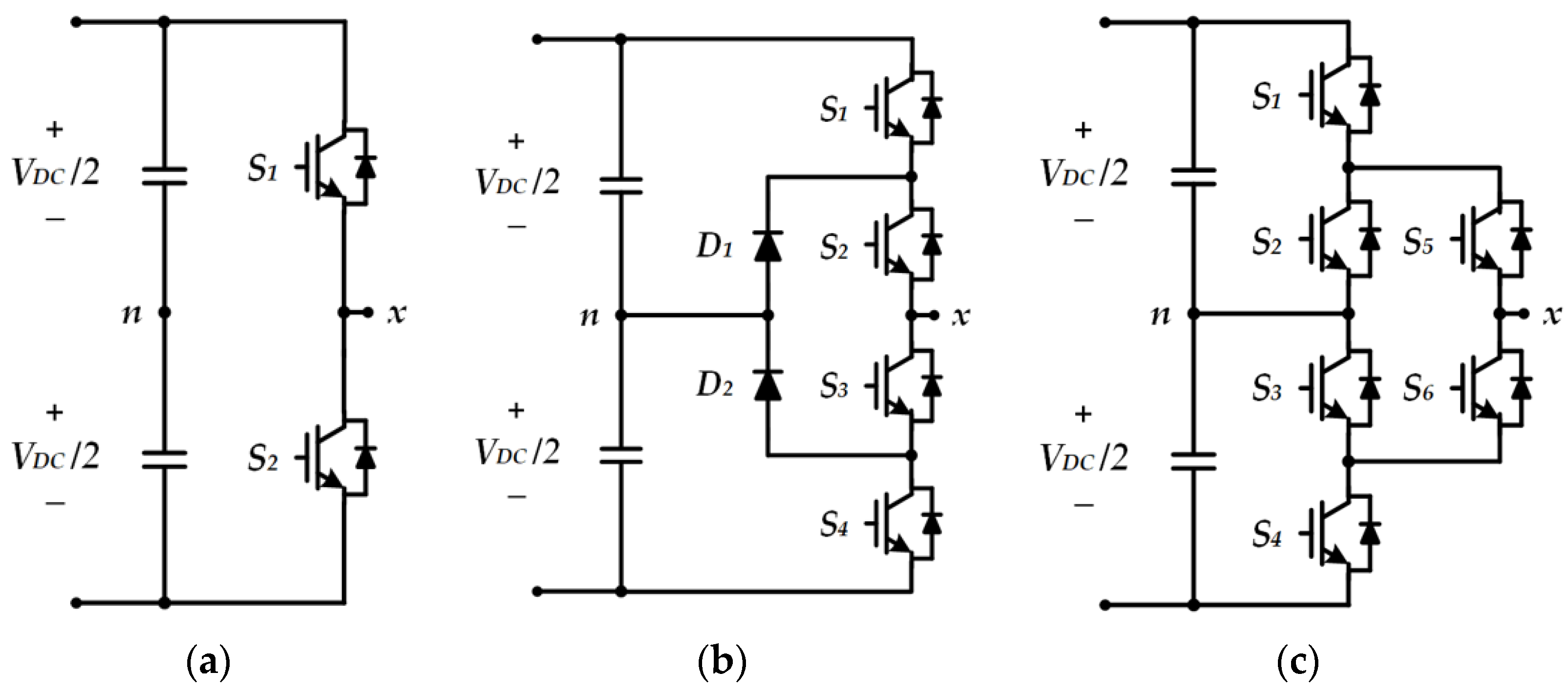
2. Si/SiC Hybrid ANPC Inverter

2.1. Circuit Configuration

Figure 2 shows three types of VSI circuit for PCS of BESS. The conventional two-level (2L) inverter, shown in Figure 2a, is the simplest power converter circuit. However, it increases DC battery voltage, as only two Si-IGBTs block the DC battery voltage. The 3L-NPC VSI was introduced in the 1980s to improve the efficiency of a motor drive system by adopting pulse width modulation (PWM) [21]. The standard 3L-NPC inverter has been widely adopted in medium-power applications owing to the higher efficiency in the power conversion. The output pole-voltage between the neutral-point (n) and the terminal (x) varies from +VDC/2 to zero or zero to –VDC/2. In the 3L-NPC inverter, the voltage variance dv/dt and harmonic components are reduced and compared with the 2L-VSI [22,23,24,25]. One leg of the standard 3L-NPC topology consists of upper and lower DC-link capacitors, four Si-IGBTs (S1, S2, S3, and S4) and two neutral-point clamping diodes (D1 and D2), as shown in Figure 2b. The power losses of switching devices are defined by the switching states and direction of current flow while the PCS converts the energy between DC and AC side. The power losses of the standard NPC inverter are concentrated on the outer-side switches (S1 and S4) when the power flows from DC to AC side. On the other hand, the inner-side switches (S2 and S3) take the burden of most power losses when the power flows from AC to DC side. The uneven distribution of power losses is a substantial disadvantage of the standard NPC topology as it results in varied junction temperature rise between the switching devices [26]. Moreover, this phenomenon is harmful to the device’s characteristics, limiting the switching frequency of power transistors.
In [26], the ANPC topology was proposed to overcome the uneven distribution loss of the standard NPC inverter. There is a remarkable difference between ANPC and NPC inverter wherein the neutral-point clamping diodes in the standard NPC are replaced with two active switching devices to form the ANPC, as shown in Figure 2c. The ANPC inverter can thus combine multiple switching states and commutations compared to the standard NPC inverter with six IGBTs (S1, S2, S3, S4, S5, and S6). However, the large power losses from Si-IGBTs continue to be a significant limitation of the Si-ANPC inverter. The active loss balancing method for Si-ANPC inverter is quite complicated, as it requires the junction temperature estimation of each Si-IGBT to select redundant zero-switching states. Therefore, this loss balancing strategy increases complexity in terms of the control system.
The HANPC topology was presented in [4] to realize high power density for a 3L-NPC inverter with SiC-MOSFETs. Figure 3 shows the circuit configuration of a grid-connected three-phase HANPC with DC power source (VDC) and filter inductor (L). Two inner-side Si-IGBTs (S5 and S6) in the Si-ANPC inverter are replaced with two SiC-MOSFETs (Q1 and Q2) in the HANPC topology. The SiC-MOSFET shows high-temperature endurance, extremely low switching loss, and high-speed switching frequency operation. The cost of SiC-MOSFETs is still higher than Si-IGBTs, and thus the HANPC inverter is a viable alternative that provides the advantages of SiC-MOSFETs with a lower cost than full SiC-NPC inverter topology. By the unique modulation method of the HANPC inverter, the switching loss is concentrated in only four SiC-MOSFETs and conduction losses are restricted to two Si-IGBTs. The basic modulation method of the HANPC inverter is introduced in the following section.

2.2. Operation Principle

In the HANPC inverter, two different switching frequencies are utilized: high-speed frequency (HF) and low-speed frequency (LF). As shown in Figure 4, the Si-IGBTs and SiC-MOSFETs take different PWM signals through the gate driver of each switching device. First, a reference phase-voltage V*xs for each leg is defined as a sinusoidal waveform. Next, an offset voltage Voffset is calculated using three-phase reference voltages. This offset voltage is added to the three-phase reference voltages to implement a simplified space vector PWM (SVPWM). After injecting the offset voltage into the reference phase-voltages, the reference pole-voltage signal V*xn is normalized and compared with a triangular carrier wave. The HF PWM signal is generated as a result of this comparison, indicating a much faster speed than the LF PWM signal. The LF PWM signal is determined by the polarity of the reference pole-voltage signal V*xn. Therefore, a period of LF PWM signal is the same as the reference voltage, indicating relatively slow operation. The Si-IGBTs repeat turning on and off with a relatively long cycle using this HF/LF PWM technique. Additionally, the operation of SiC-MOSFETs is controlled complementarily, turning on and off states by HF PWM signals.
As represented in Table 1 and Figure 5, there are four different switching states and three different output voltages in the HANPC inverter. Two Si-IGBTs are paired up and turn on and off together (S1/S3 and S2/S4). When two Si-IGBTs are turned off, the other two Si-IGBTs are turned on. The fundamental period is the same as a reference voltage signal for each phase. The duty of the LF PWM signal is 50% for all time, meaning that Si-IGBTs remain turned-on during half of one period. The SiC-MOSFETs conduct relatively rapid switching operations by HF PWM signals with the varying duty ratio. Based on the combination of status in each switch, four switching states are defined in the HANPC inverter. While the reference voltage is positive, a positive (P) and zero (O+) states are modulated. If one leg is on the P state, current can flow through upper-side Si-IGBT S1 and SiC-MOSFET Q1. The O+ state is made by changing the switching state of two SiC MOSFETs. On the other hand, a negative (N) and another zero (O–) states are produced during the negative reference voltage. In the N state of HANPC inverter, a negative current flows through the channel of lower-side, SiC-MOSFET Q2 and Si-IGBT S4. The N and O– states change from one to the other by turning on and off the SiC-MOSFETs. The output pole voltage is generated with three different voltage levels: +VDC/2, 0, and –VDC/2. Two SiC-MOSFETs are operating at a high speed, but the switching losses are extremely low compared to the Si-IGBTs, which is an advantage of WBG switching devices. Eventually, almost the same losses may be generated in the six active switches of the HANPC inverter.

3. Proposed Fault Diagnosis Method for Open-Switch Fault Condition

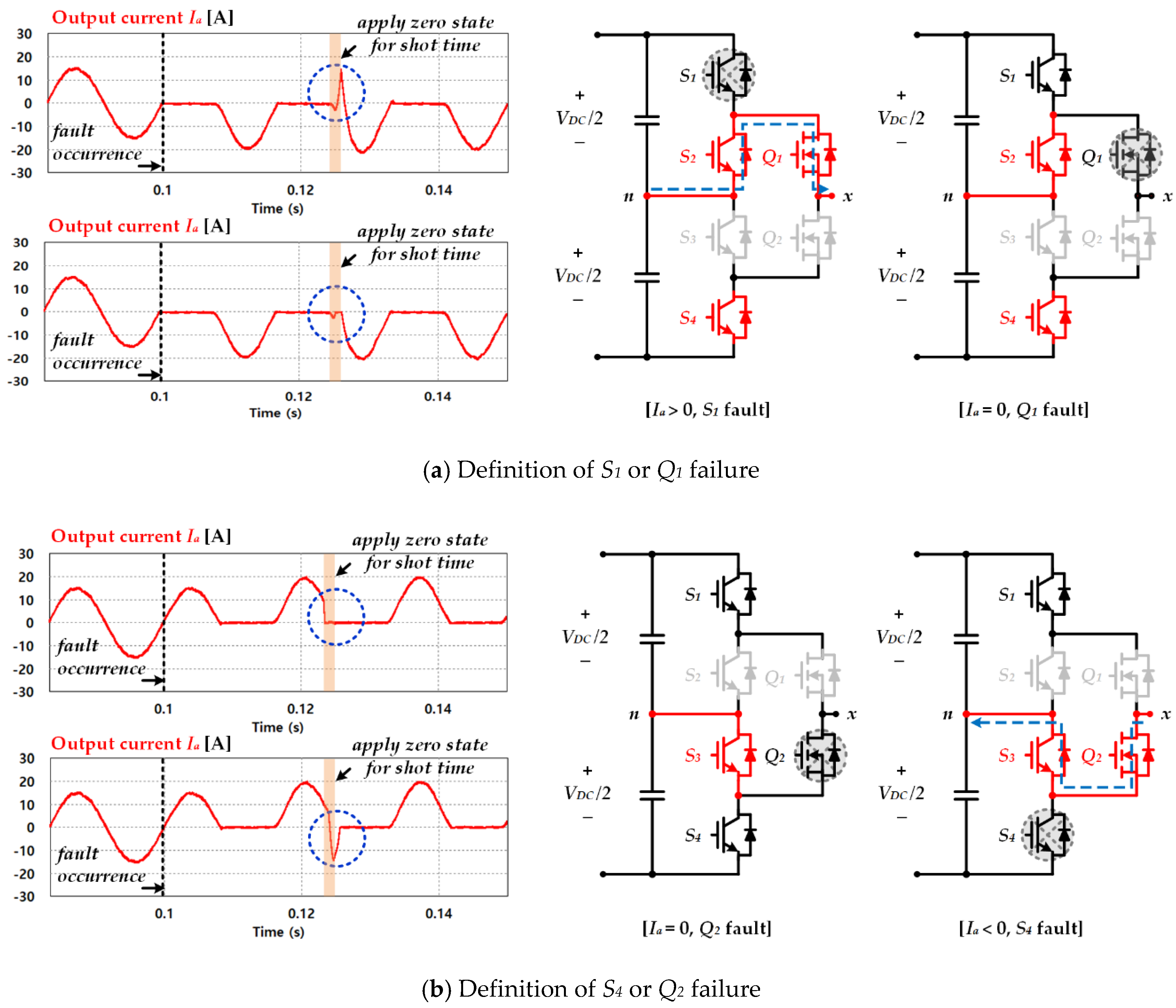
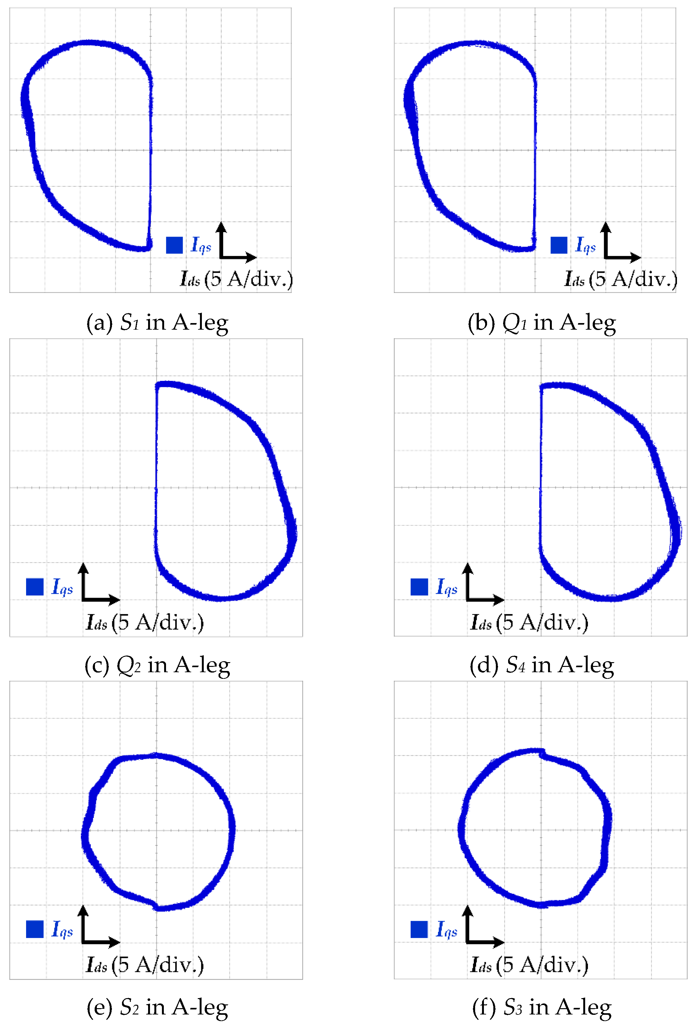
3.1. Analysis of Open-Switch Faults in Six Switches

The open-switch fault conditions of six switching devices in the HANPC inverter are drawn, as shown in Figure 6. The open-switch faults mostly occur due to accumulated thermal stress in the switching device. The failure mechanism of the power transistor module is shown in [27], including an open circuit and other catastrophic failures. As marked in each case, if any open-switch fault occurs and an open circuit is configured in a leg, the current cannot flow normally and is severely distorted. If there is any open-switch fault in a leg of the HANPC inverter while the other legs are normal, the phase current of the faulty leg is distorted.
The distortions of phase current have some patterns and indicate the location of the open-switch fault. If the open-switch fault occurs in one of the upper-side switches (S1 or Q1), the positive switching state is not generated. This means that the positive current cannot flow through the upper-side current path during half the cycle of a fundamental period. In this case, the output current of the half period is zero, but the other half remains unaffected by the open-switch fault. Conversely, if the open-switch fault occurs in one of the lower-side switches (S4 or Q2), the negative current does not flow through the lower-side current path. Similar to the previous case, the output current of the half period is zero, but the other half remains unaffected by the open-switch fault. If the open-switch fault occurs in one of the two neutral-point active switches (S2 or S3), the respective zero-switching state is not generated and the current path is not connected from the neutral-point of DC-link capacitors to the output terminal point of the HANPC inverter. When S2 is in the faulty condition, the O– switching state is not made and the negative current is distorted partially.
Contrary to the failures in the other lower-side switches, only some portion of the negative current is distorted. The positive cycle of output current is unaffected by the open-switch fault of S2. When S3 fails, the faulty condition is opposite to the faulty S2 condition. The O+ switching state is affected by the faulty switch during the positive half cycle of the leg, and thus the positive current is distorted.
Figure 7 shows the output currents in a three-phase coordinate system and in a stationary reference frame and explains the Park’s transformation. These three-phase output currents are expressed into direct-quadrant (dq) axis currents by Park’s transformation, and its radius is calculated as follows:
I d s = 2 I a I b I c 3 ,   I q s = I b I c 3
r = I d s 2 + I q s 2
The calculated Park’s vector rotates in dq-axis, and its trace forms a current pattern. In the healthy condition, the current pattern draws a perfect circular shape as shown in Figure 7c and maintains a constant radius r. The variation of r is an indicator of fault detection. Additionally, the location of the central point is also an evaluation factor. The coordinate value (Ids,cen, Iqs,cen) of the central point is calculated as the average value of a minimum and maximum value as follows:
( I d s , c e n , I q s , c e n ) = ( I d s , max + I d s , min 2 , I q s , max + I q s , min 2 )
The central point (Ids,cen, Iqs,cen) is drawn, as shown in Figure 7c. When the HANPC inverter operates in healthy condition, the central point of the trace is located at (0, 0). If S1 in A-leg has failed, the location of the central point moves as shown in Figure 7d. The angular value of the central point θcen is expressed in a polar coordinate system as follows:
θ c e n = tan 1 ( I q s , c e n / I d s , c e n )

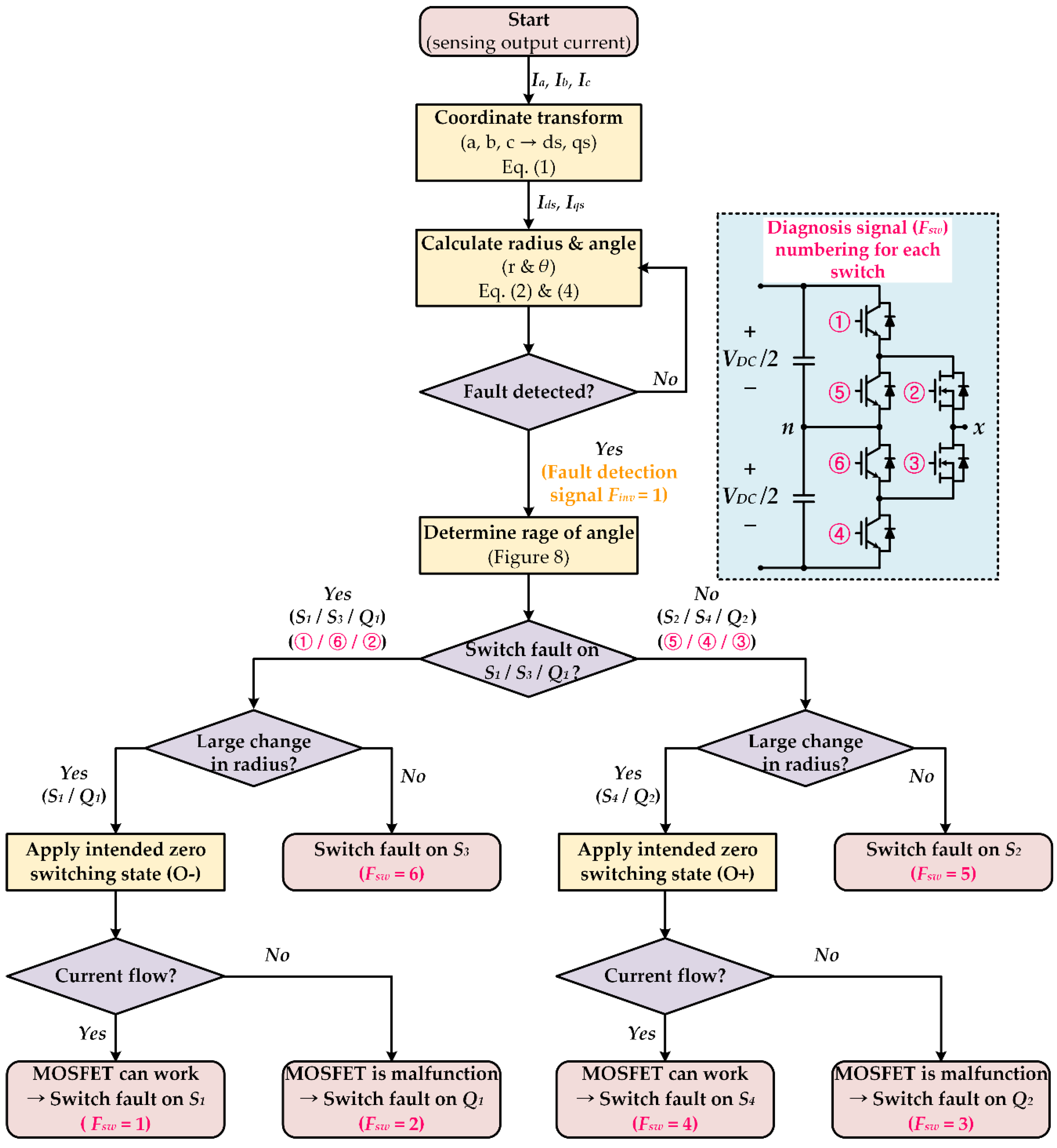
3.2. Fault Detection and Diagnosis Method of Open-Switch Fault

As explained in the previous section, if one of the switching devices fails and an open circuit is generated, the phase current’s magnitude is halved or reduced. Under the effect of the current controller, which follows the reference current value, the output current of the other healthy legs becomes larger than under normal conditions in order to maintain the magnitude of reference current value and overall power delivery. The distortion and variation of magnitude also affect the dq-axis current directly, and fluctuations are induced in the radius r and angular location of the central point θcen. The variation of the radius r and angle θcen are critical factors for fault detection if the dq-axis currents are expressed in the current pattern. This implies that the distorted current patterns include the information pertaining to the location of the failed switching device in the HANPC inverter.
The faulty condition signal of the HANPC inverter (Finv) is easily detected by monitoring the radius in the current pattern. The detection method for the failed switch (Fsw) consists of the following process. First, the radius of the current pattern is monitored to detect a fault in a specific leg of the HANPC inverter. The radius, r, is calculated as given in Equation (2) and does not change when the HANPC inverter generates a pure sinusoidal output current. If there is an open-switch failure, the current pattern is distorted, as shown in Figure 8, and the radius fluctuates. The angular position of the central point, θcen, is used to identify the faulty leg as derived in Equation (4). If S1 has failed for each leg, it is expected that the central point is moved to a specific area according to the faulty leg and its location is monitored by means of θcen. It is possible to define whether the open-switch fault lies in the upper- or lower-side switches of the faulty leg by monitoring the range of radius r. As listed in Figure 8, the current distortion of each phase occurs at different angles of the current pattern according to the location of the faulty switching device and these angles and radii help find the specific location of the faulty switch. The variation of the current pattern can be standardized according to the faulty switches. As listed in Figure 8, the open-switch fault in A-leg causes current pattern distortion in the left half-plain (Figure 8a,c) or right plain (Figure 8b,d). This is because the A-phase current value is implied by when the radius is located in the horizontal line (Ids axis). However, if the faulty switch occurs in B-leg, we should consider 120° skew angle. Likewise, when the radius r is decreased in 120° or 300° regions, this means distortion in B-phase current. This if obvious in Figure 8e–h. For example, if the positive current of B-phase is distinguished by the open-switch fault of S1 in B-leg (Figure 8e), the current pattern gets half the 120°-biased shape compared with S1 fault in A-leg (Figure 8a). The case of C-leg fault is similar to discrimination of the other leg’s fault. As presented in Figure 8i–l, the open-switch fault of C-leg makes distorted current patterns only 240°-biased compared with A-leg’s fault. The fault in each leg of HANPC makes different values of (Ids,cen, Iqs,cen) and also affects angle θcen. The failures in upper-side switches (S1 or Q1) and lower-side switches (S4 or Q2) are clearly distinguished by monitoring the angle θcen and r when the magnitude of the current pattern becomes zero. The open-switch fault in the neutral-side switches (S2 or S3) causes a relatively small variation in the current pattern. However, it is sufficiently distinguishable. As shown in Figure 8a,d, the open-switch faults on the same-side S1, Q1 (or S4, Q2) generate the same current patterns as that described by a semicircle. This is because of the impossibility of the P or N switching state in the faulty leg, whether the failure is in Si-IGBT or SiC-MOSFETs. Therefore, the final step requires an additional switching injection to diagnose the exact location of the faulty switch. As mentioned earlier, the distortion analysis of the current pattern is not sufficient to diagnose the exact location of the fault amid the two candidates, for example, S1 and Q1. However, there are critical differences between the Si-IGBT and the SiC-MOSFET fault. The zero-switching state can distinguish these two kinds of single switch failure. When it comes to the grid-connected system, there are three-phase grid voltage sources. Therefore, current flows are determined depending on the relationship between the grid voltage Vxs and the output pole voltage Vxn. As presented in Figure 9, it is possible to distinguish between the two upper- or lower-side switches even though they demonstrate the same current pattern by injecting a zero-switching state. When S1 fails and Q1 does not, a current spike is induced by injecting the intended zero-switching state for a short time as it generates the current path through Q1, between the neutral-point of the DC-link and output terminal. The faulty switch signal Fsw is therefore marked as Fsw = 1 to represent the faulty S1 condition when the current spike is measured by applying the zero-switching state. On the other hand, if the SiC-MOSFET Q1 fails, the zero-switching does not affect the output current and Fsw is marked as Fsw = 2. Here, the faulty S1, Q1, Q2, and S4 switches are marked as 1, 2, 3, and 4, respectively, for the Fsw signal, whereas the faulty S2 and S3 switches are marked as 5 and 6, respectively. Finally, all the faulty conditions for six different switches are detected and distinguished by the proposed diagnosis method. The overall flowchart of the fault detection method is illustrated in Figure 10.

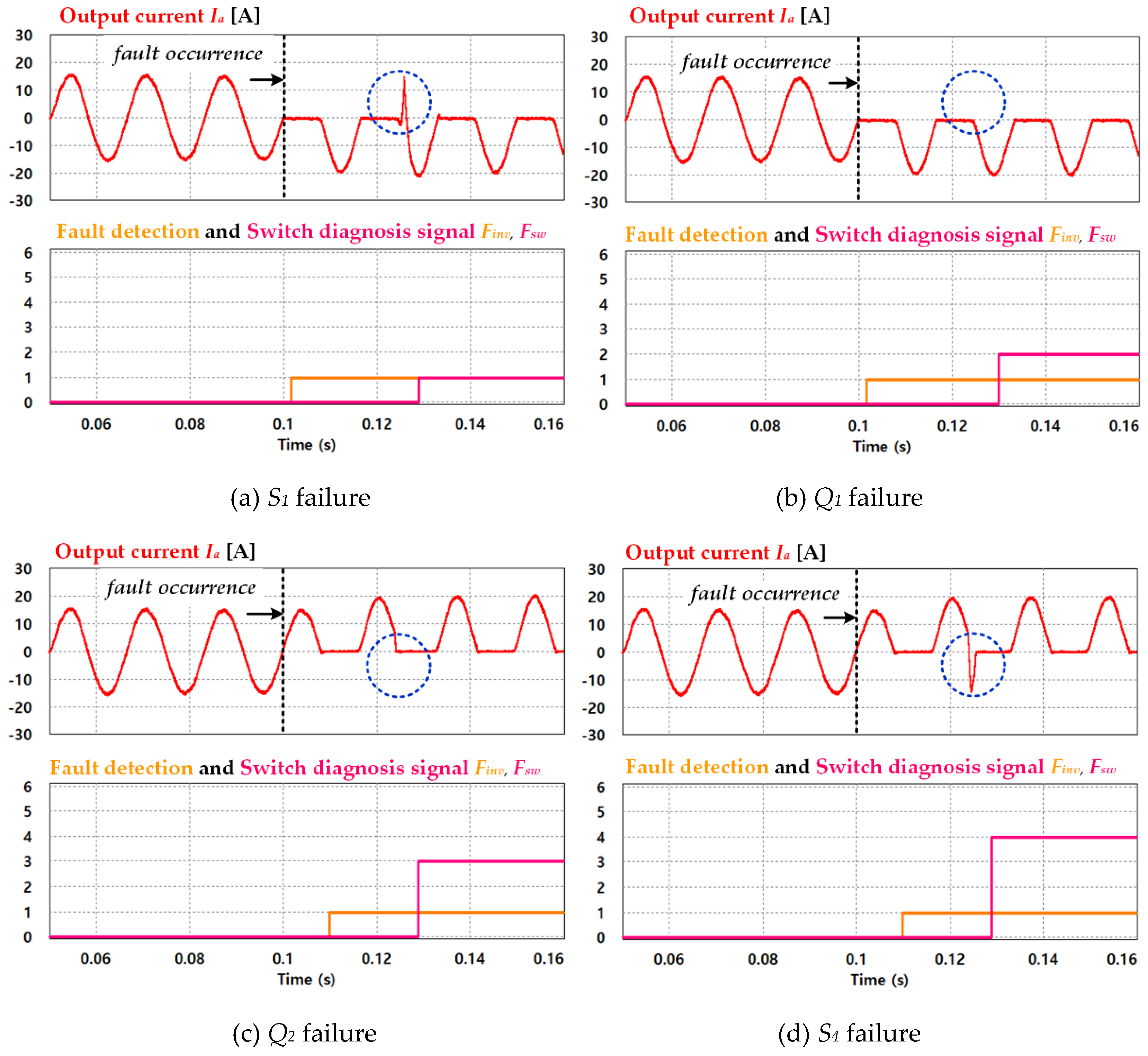
4. Simulation Results

To confirm the validity of the proposed diagnostic method, several simulations were conducted. The circuit diagram and simulation parameters are shown in Figure 3 and Table 2.
Figure 11 shows the simulation results of the proposed diagnostic method for the open-switch fault in the HANPC inverter. The faulty condition assumes that a single switch in A-phase has failed, and the numbering for each switch failure is presented in Figure 10. Each waveform of Figure 11 shows an A-phase output current and the fault signals indicating whether the inverter is faulty (Finv) and which switch is faulty (Fsw). While the output current is controlled at the constant amplitude of 15 A, the open-switch fault occurs at 0.1 s. From then on, the output current is distorted and the yellow detection signal rises quickly (Finv = 1). As explained in Section 3.2, the upper-side switch (S1 and Q1) fault produces the same current distortion, and the current spike is an indicator of Si-IGBT S1 failure. After applying the zero-switching state, the diagnosis signal is generated with the specific number indicating the location of the faulty switch. This zero-switching injection is used to diagnose the faulty lower-side switch identically when the negative current is not generated. In the condition of Finv = 1, the zero-switching state is applied to identify which switch is faulty among Q2 (Fsw = 3) and S4 (Fsw = 4). If the negative spike current is induced in the phase current, it implies that the current must be passed through Q2, and the faulty switch is S4 (Fsw = 4). The fault occurring in the neutral-point IGBT switch S2 (Fsw = 5) and S3 (Fsw = 6) is detected by current patterns without the zero-switching injection.

5. Experimental Results

The proposed method was implemented in a three-level grid-connected HANPC inverter. The experimental parameters are listed in Table 2. Figure 12 shows the experimental setup of the grid connected HANPC inverter. The experimental equipment was composed of a DC power source (TC.P.20.600.400 from REGATRON), AC grid simulator (MX30 from California Instruments), three-phase HANPC inverter, and a control board. The HANPC inverter is composed of a Si-IGBT module (SK75GBB066T from Semikron) and discrete-type SiC-MOSFETs (C2M0040120D from CREE). The control board was based on a digital signal processor (TMS320F28377S from Texas Instruments).
An oscilloscope (HDO6104 of Teledyne LeCroy) was used to measure and print out the instantaneous current, voltage, and fault signals. Figure 13 shows the measured current patterns within a stationary reference frame, where the horizontal axis is Ids, and the vertical axis is Iqs. The radius r of the current pattern is 10 A and depicts a perfectly circular shape in the healthy condition, and the figure provides six types of open-switch faults in the A-phase. When the open-switch fault occurs in the upper-side switches (S1 or Q1), the positive value of the Ids current is not generated. Therefore, the right half-plane of the current pattern is reduced, but the left half of the circle becomes more substantial. Therefore, the central point of the current pattern is located on the left-side plane.
On the other hand, when the open-switch fault occurs in the lower-side switches (S4 or Q2), the left half-plane of the current pattern is not generated, and the central point is located on the right-side plane. When the neutral-point switch fails, there is little fluctuation in the radius by means of the slight distortion. The measured current patterns are almost the same for the simulation results and the radius and angular values are used to detect the open-switch fault.
Figure 14 shows the experimental result of the proposed fault diagnosis method. A black dotted line separates the healthy and faulty condition of the HANPC inverter. Before the open fault occurred, the output current is controlled at the constant amplitude of 10 A with a zero value of fault signals (Finv = Fsw = 0). After the open-fault occurs, the A-phase output current is distorted. The distortion has different characteristics depending on the location of the fault. However, the information from current patterns is insufficient to diagnose the accurate fault location, as shown in Figure 13a. When there are two possible options of Fsw = 1 or Fsw = 2, the current spike decides to switch the diagnosis signal as shown in Figure 14a,b. In the other ambiguous situation, as shown in Figure 14c,d, the negative spike current helps identify the fault location between Fsw = 3 or Fsw = 4. Figure 14e,f show slight distortions in the output currents attributed to the open-switch fault in Si-IGBT S2 and S3. In about six types of fault conditions, the fault detection signal has arisen in less than one fundamental period and the switch diagnosis signal has been generated accurately for each case. Therefore, the experimental results guarantee that the proposed method performs the diagnosis of the open-switch fault diagnosis well in the case of the HANPC inverter.

6. Conclusions

An open-switch fault diagnosis method for the grid-connected HANPC inverter for the BESS is proposed in this paper. The HANPC inverter provides higher performance using additional SiC-MOSFETs with Si-IGBTs. To improve the reliability of the HANPC inverter, the proposed fault diagnosis method performs outstanding fault detection without the need for additional hardware or sensors which require the extra cost and maintenance. The whole diagnostic procedures have advantages because of being implemented with only three-phase current sensors and simple embedded software techniques with accurate and fast fault-detection performance. The methodology is based on the analysis of the dq-axis current in the stationary reference frame. The current trace draws the current pattern in the stationary reference frame. The distortion of the current pattern includes information regarding the faulty switching device and its location. To distinguish the Si-IGBT fault or SiC-MOSFET fault, the proposed method applies the injection of a zero-switching state. The zero-switching state injection detects the exact location of the faulty switching device, and the corresponding spike in current is monitored. The faulty condition of all six switching devices is analyzed, and the various simulation and experimental results demonstrate the feasibility and performance of the proposed fault diagnostic method.

Author Contributions

K.-B.L. provided guidance and supervision. S.-M.K. built a hardware set-up and administrated this project. S.-H.K. performed the simulation, experiment. B.H.K. conceived the idea and methodology of this paper and wrote the paper and revised the manuscript as well. All authors have equally contributed to the simulation analysis, experiment and result discussions. All authors have read and agreed to the published version of the manuscript.

Funding

This work was supported by the Korea Institute of Energy Technology Evaluation and Planning (KETEP) and the Ministry of Trade, Industry & Energy (MOTIE) of the Republic of Korea. (No. 20171210201100, No. 20182410105160).

Acknowledgments

Authors thank our Power Electronics Laboratory colleagues of Electrical & Computer Engineering Department, Ajou University, South Korea.

Conflicts of Interest

The authors declare no conflict of interest.

References

  1. Lee, K.B.; Lee, J.S. Reliability Improvement Technology for Power Converters, 1st ed.; Springer: Singapore, 2017; ISBN 978-981-10-4991-0. [Google Scholar]
  2. Ballal, M.S.; Bhadane, K.V.; Moharil, R.M.; Suryawanshi, H.M. A Control and Protection Model for the Distributed Generation and Energy Storage Systems in Microgrids. J. Power Electron. 2016, 16, 748–759. [Google Scholar] [CrossRef] [Green Version]
  3. Sung, W.-Y.; Ahn, H.M.; Oh, C.-Y.; Lee, B.K. Design and Control of a Bidirectional Power Conversion System with 3-level T-type Inverter for Energy Storage Systems. J. Electr. Eng. Technol. 2018, 13, 326–332. [Google Scholar] [CrossRef]
  4. Guan, Q.-X.; Li, C.; Zhang, Y.; Wang, S.; Xu, D.-D.; Li, W.; Ma, H. An Extremely High Efficient Three-Level Active Neutral-Point-Clamped Converter Comprising SiC and Si Hybrid Power Stages. IEEE Trans. Power Electron. 2018, 33, 8341–8352. [Google Scholar] [CrossRef]
  5. Millán, J.; Godignon, P.; Perpiñà, X.; Pérez-Tomás, A.; Rebollo, J. A Survey of Wide Bandgap Power Semiconductor Devices. IEEE Trans. Power Electron. 2014, 29, 2155–2163. [Google Scholar] [CrossRef]
  6. Anthon, A.; Zhang, Z.; Andersen, M.A.; Holmes, D.G.; McGrath, B.; Teixeira, C.A. The Benefits of SiC MOSFETs in a T-Type Inverter for Grid-Tie Applications. IEEE Trans. Power Electron. 2017, 32, 2808–2821. [Google Scholar] [CrossRef] [Green Version]
  7. Kwon, B.H.; Kim, S.-H.; Bea, K.-C.; Lee, K.-B. Performance Analysis on a Bidirectional Operation of a Three-Level Hybrid ANPC Inverter. Trans. Korean Inst. Electr. Eng. 2019, 10, 1204–1213. [Google Scholar] [CrossRef]
  8. Choi, U.-M.; Lee, J.-S. Condition Monitoring of Reliability-Critical Components in Power Electronic Systems. Trans. Korean Inst. Power Electron. 2019, 24, 244–258. [Google Scholar] [CrossRef]
  9. Yang, S.; Xiang, D.; Bryant, A.; Mawby, P.; Ran, L.; Tavner, P. Condition Monitoring for Device Reliability in Power Electronic Converters: A Review. IEEE Trans. Power Electron. 2010, 25, 2734–2752. [Google Scholar] [CrossRef]
  10. Lee, E.; Lee, K.-B. Fault-Tolerant Strategy to Control a Reverse Matrix Converter for Open-Switch Faults in the Rectifier Stage. J. Power Electron. 2016, 16, 57–65. [Google Scholar] [CrossRef] [Green Version]
  11. Choi, U.-M.; Lee, J.-S.; Blaabjerg, F.; Lee, K.-B. Open-Circuit Fault Diagnosis and Fault-Tolerant Control for a Grid-Connected NPC Inverter. IEEE Trans. Power Electron. 2016, 31, 7234–7247. [Google Scholar] [CrossRef]
  12. Li, J.; Huang, A.Q.; Liang, Z.; Bhattacharya, S. Analysis and Design of Active NPC (ANPC) Inverters for Fault-Tolerant Operation of High-Power Electrical Drives. IEEE Trans. Power Electron. 2012, 27, 519–533. [Google Scholar] [CrossRef]
  13. Lee, J.-S.; Lee, K.-B.; Blaabjerg, F. Open-Switch Fault Detection Method of a Back-to-Back Converter Using NPC Topology for Wind Turbine Systems. IEEE Trans. Ind. Appl. 2015, 51, 325–335. [Google Scholar] [CrossRef]
  14. Ko, Y.J.; Lee, K.B. Fault Diagnosis of a Voltage-Fed PWM Inverter for a Three-parallel Power Conversion System in a Wind Turbine. J. Power Electron. 2010, 10, 686–693. [Google Scholar] [CrossRef]
  15. Kim, T.-J.; Lee, W.-C.; Hyun, D.-S. Detection Method for Open-Circuit Fault in Neutral-Point-Clamped Inverter Systems. IEEE Trans. Ind. Electron. 2009, 56, 2754–2763. [Google Scholar] [CrossRef]
  16. Afef, B.-B.A.; Hafedh, B.A.; Frédéric, R.; Jean-Marc, B.; Franck, M.; Ilhem, S.-B. Versatile Three-Level FC-NPC Converter With High Fault-Tolerance Capabilities: Switch Fault Detection and Isolation and Safe Postfault Operation. IEEE Trans. Ind. Electron. 2019, 64, 6453–6464. [Google Scholar] [CrossRef]
  17. Qun-Tao, A.; Li-Zhi, S.; Ke, Z.; Li, S. Switching Function Model-Based Fast-Diagnostic Method of Open-Switch Faults in Inverters Without Sensors. IEEE Trans. Power Electron. 2011, 26, 119–126. [Google Scholar] [CrossRef]
  18. Fazio, P.; Marchesoni, M.; Parodi, G. Fault detection and reconfiguration strategy for ANPC converters. In Proceedings of the 2012 15th International Power Electronics and Motion Control Conference (EPE/PEMC), Novi Sad, Serbia, 4–6 September 2012. [Google Scholar] [CrossRef]
  19. Cardoso, A.M.; Saraiva, E.S. Computer-aided detection of airgap eccentricity in operating three-phase induction motors by Park’s vector approach. IEEE Trans. Ind. Appl. 1993, 29, 897–901. [Google Scholar] [CrossRef]
  20. Choi, U.-M.; Jeong, H.-G.; Lee, K.-B.; Blaabjerg, F. Method for Detecting an Open-Switch Fault in a Grid-Connected NPC Inverter System. IEEE Trans. Power Electron. 2012, 27, 2726–2739. [Google Scholar] [CrossRef]
  21. Nabae, A.; Takahashi, I.; Akagi, H. A New Neutral-Point-Clamped PWM Inverter. IEEE Trans. Ind. Appl. 1981, IA-17, 518–523. [Google Scholar] [CrossRef]
  22. Rodriguez, J.; Bernet, S.; Steimer, P.K.; Lizama, I.E. A Survey on Neutral-Point-Clamped Inverters. IEEE Trans. Ind. Electron. 2010, 57, 2219–2230. [Google Scholar] [CrossRef]
  23. Kim, S.-M.; Won, I.J.; Kim, J.; Lee, K.-B. DC-Link Ripple Current Reduction Method for Three-Level Inverters with Optimal Switching Pattern. IEEE Trans. Ind. Electron. 2018, 65, 9204–9214. [Google Scholar] [CrossRef]
  24. Lee, J.-S.; Yoo, S.; Lee, K.-B. Novel Discontinuous PWM Method of a Three-Level Inverter for Neutral-Point Voltage Ripple Reduction. IEEE Trans. Ind. Electron. 2016, 63, 3344–3354. [Google Scholar] [CrossRef]
  25. Schweizer, M.; Friedli, T.; Kolar, J.W. Comparative Evaluation of Advanced Three-Phase Three-Level Inverter/Converter Topologies Against Two-Level Systems. IEEE Trans. Ind. Electron. 2013, 60, 5515–5527. [Google Scholar] [CrossRef]
  26. Brückner, T.; Bernet, S.; Güldner, H. The active NPC converter and its loss-balancing control. IEEE Trans. Ind. Electron. 2005, 52, 855–868. [Google Scholar] [CrossRef]
  27. Choi, U.-M.; Blaabjerg, F.; Jørgensen, S. Power Cycling Test Methods for Reliability Assessment of Power Device Modules in Respect to Temperature Stress. IEEE Power Electron. 2018, 33, 2531–2551. [Google Scholar] [CrossRef] [Green Version]
Figure 1. Basic configuration of a grid-connected battery energy storage system (BESS).
Electronics 09 00399 g001
Figure 2. Three types of voltage source inverters: (a) two-level (2L)-inverter; (b) standard 3L-NPC (three-level neutral-point clamped) inverter; (c) active NPC inverter.
Electronics 09 00399 g002
Figure 3. Circuit configuration of a three-phase grid-connected hybrid active NPC (HANPC) inverter.
Electronics 09 00399 g003
Figure 4. Operation principle of HANPC inverter: (a) reference voltages for space vector pulse width modulation (SVPWM); (b) normalized reference voltage; (c) PWM signals of high-speed frequency (HF) and low-speed frequency (LF); (d) gate signals for silicon-based insulated-gate bipolar transistors (Si-IGBTs) and silicon carbide metal-oxide-semiconductor field-effect transistors (SiC-MOSFETs) in HANPC inverter.
Electronics 09 00399 g004
Figure 5. Switching states and current path of HANPC inverter: (a) positive state P; (b) positive zero state O+; (c) negative zero state O–; (d) negative state N.
Electronics 09 00399 g005
Figure 6. Current path and three-phase current according to different faulty condition in a leg of the HANPC inverter.
Electronics 09 00399 g006
Figure 7. Output current waveforms and current pattern drawn by current vector.
Electronics 09 00399 g007aElectronics 09 00399 g007b
Figure 8. Current patterns according to different faulty condition (healthy condition: r = 15 A).
Electronics 09 00399 g008aElectronics 09 00399 g008b
Figure 9. Distinguishing process of faulty switch in Si-IGBT or SiC-MOSFET by injecting zero-switching state.
Electronics 09 00399 g009
Figure 10. Flowchart of the proposed fault diagnostic method for open-switch failure in the HANPC inverter.
Electronics 09 00399 g010
Figure 11. Simulation results of the open-switch fault detection with A-leg current waveform.
Electronics 09 00399 g011aElectronics 09 00399 g011b
Figure 12. Experimental set-up of three-phase grid-connected HANPC inverter.
Electronics 09 00399 g012
Figure 13. Measured current patterns according to faulty condition.
Electronics 09 00399 g013
Figure 14. Measured current waveforms and fault detection signals.
Electronics 09 00399 g014
Table 1. Switching states based on the switch status of the HANPC inverter.
Switching StateOutput Pole Voltage VxnS1S2S3S4Q1Q2
Positive (P)+VDC/2ONOFFONOFFONOFF
Zero (O+)0ONOFFONOFFOFFON
Zero (O–)0OFFONOFFONONOFF
Negative (N)VDC/2OFFONOFFONOFFON
Table 2. Parameters for simulation and experiments.
ParametersValueUnit
Voltage of DC-link (VDC)600V
Line-to-line grid voltage380Vrms
Capacitance of DC-link (Chigh, Clow)4700μF
Grid filter inductance (L)1mH
Switching frequency of SiC-MOSFET20,000Hz
Switching frequency of Si-IGBT50Hz

