Article

EMI Susceptibility of the Output Pin in CMOS Amplifiers

Department of Information Engineering, University of Brescia, 25123 Brescia BS, Italy
*
Author to whom correspondence should be addressed.
Electronics 2020, 9(2), 304; https://doi.org/10.3390/electronics9020304
Submission received: 16 January 2020 / Revised: 3 February 2020 / Accepted: 5 February 2020 / Published: 9 February 2020
(This article belongs to the Special Issue Electromagnetic Interference and Compatibility)

Abstract

:
Measurements in commercial devices demonstrate a considerable susceptibility of the operational amplifiers to the electromagnetic interferences coupled to their output pin. This paper investigates some basic architectures starting from single stage amplifiers up to a whole operational amplifier. The result is a correlation between the different amplifier configurations, the output impedance and the susceptibility to the interferences. The simulations are perfomed by using the standard CMOS UMC 180nm technology and by running the netlist of the schematics extracted from the layout.

1. Introduction

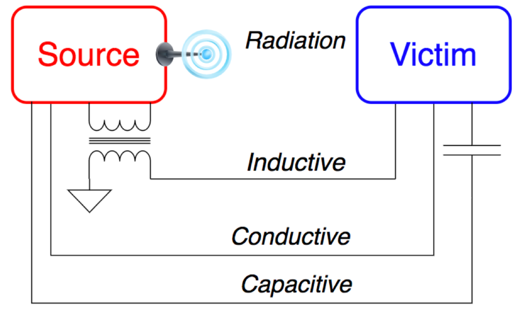
The assessment of IC immunity to EMI is presently compulsory for many applications, because, thanks to the progress of VLSI, electronics is ubiquitous. It is evident in the following industries: computing, communication, manufacturing, transport, entertainment, business, health. We can find ICs nearly everywhere: in computers (of course), in cellphones, watches, medical devices, cars.... Moreover, in recent years, raises serious preoccupations on the vulnerability of electronic equipment to intentional EMI attacks [1,2,3,4,5]: sources capable of producing very high RF power over a wide frequency range are, indeed, presently easily available or even home-made manufacturable. In general, as shown in Figure 1 and Figure 2, Electromagnetic Compatibility issues can be divided into two parts: emissions and susceptibility. Both of them should be as low as possible. This paper will focus on susceptibility, in particular of the analog ICs to conducted interferences. Due to the small dimensions of Integrated Circuits indeed, susceptibility and emission via conduction are more important than via radiation. The susceptibility of analog integrated circuits to conducted EMI has been modelled and verified with simulations as well as experimentally in several works, and analytical models predicting high-power EMI effects in CMOS operational amplifiers and offering a good matching with experimental results have been presented in [6]. On the other hand, the exact repercussion of electromagnetic interference (EMI), which is injected conductively into arbitrary pins of an integrated circuit (IC), is very hard to predict owing to the fact that all the existing coupling paths need to be taken into account [7]. Several works can be found in the literature, describing the susceptibility of analog ICs, as these are more sensitive to EMI. Most of this research focuses on operational amplifiers and other widely used analog blocks, such as for example voltage references, because of their high sensitivity to EMI and their prevalence in electronic circuits [8,9,10,11,12,13,14,15]. The EMI signals are considered directly injected into the gate of the differential pair or into the power supply pins (Vdd and Vss). On the other hand, all the pins can be a possible injection point as demonstrated, for example in [16], where the susceptibility of a bulk-driven CMOS amplifier is investigated by injecting the interferences into the bulk pin. Moreover, the direct injection of the interferences is not the only path available for the EMI. Indeed in [17], the interferences reach the IC (a Local Interconnect Network (LIN) integrated output driver) by means of a parasitic capacitive coupling between the output pin and the conductive ground plane. The unwanted RF signals may indeed be transmitted through the copper plane, often shared with other analog, digital or mixed ICs, and can be capacitively coupled to all the pins, including the output one [18,19,20].
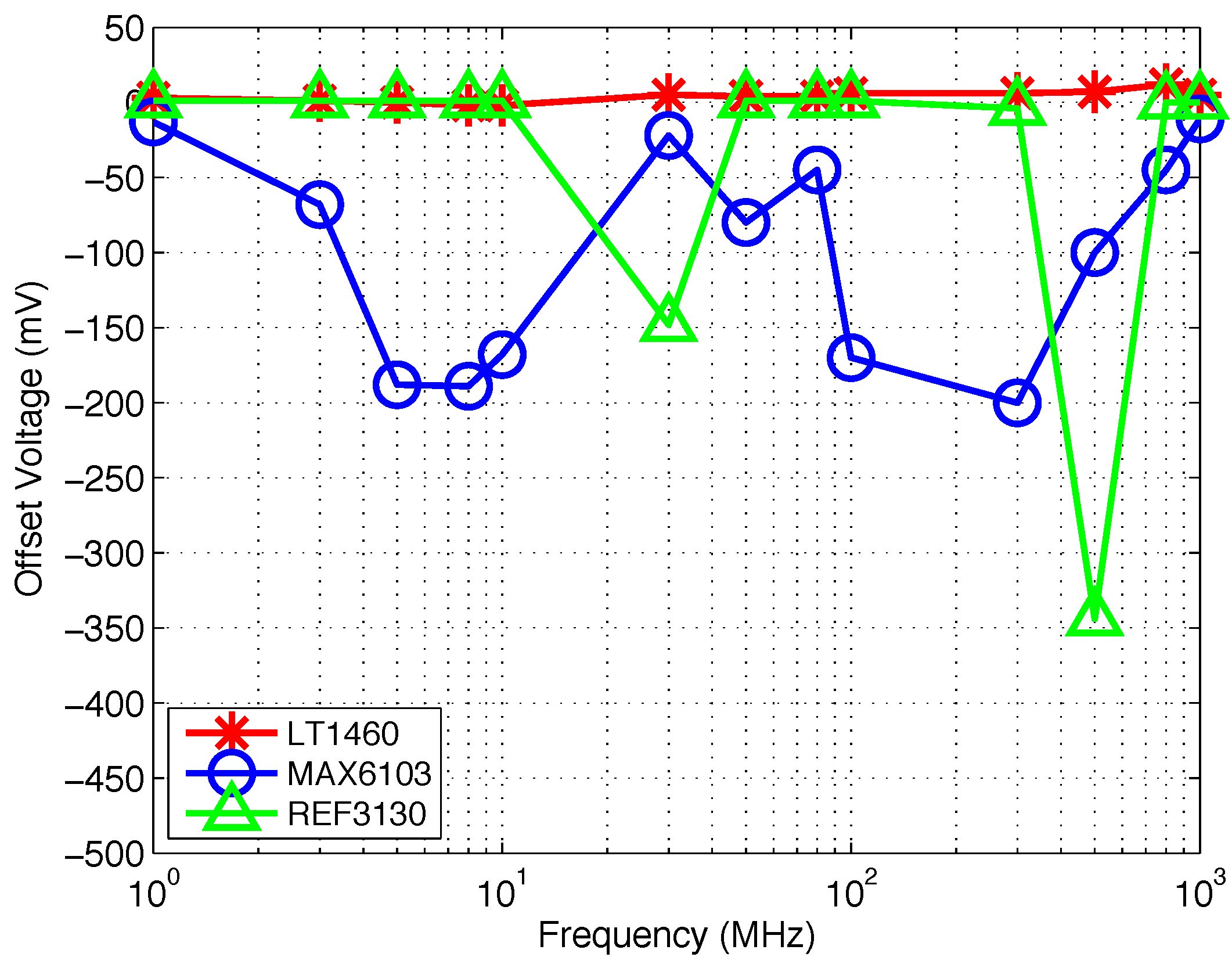
Precisesly, the susceptibility of the Operational Amplifiers to the Electromagnetic Interferences capacitively coupled to the ouput pin has been demonstrated in recent works [18,19,20], involving both commercial amplifiers and custom CMOS integrated ones. The results show a considerable vulnerability and exacerbate the scenario of EMI pollution. Moreover, it follows that the PCB ground plane, commonly shared with other analog, digital or mixed-signal circuits, can be a critical point of EMI pickup and injection. For the sake of clarity, the most relevant measurement results, provided by the literature [18,19], are plotted in Figure 3, Figure 4, Figure 5, Figure 6, Figure 7 and Figure 8. The first four graphics show the EMI induced offset in well-known commercial amplifiers (ua741, OPA705, NE5534 and ICL7611). We can see that regardless the techonology and the architecture of the amplifiers (bipolar, CMOS or BiCMOS), they are all suscpetible to the interferences coupled to the output pin. Also, the offset is very high around the hundreds of MHz and it depends on the amplitude of the interferences. The second couple of figures refers to some commercial voltage references. They are very sensible to the EMI coupled to the output pin.
Therefore, it is of paramount importance to deeply understand the reason of the susceptibility, the possible injection paths and the differences between the amplifier configurations. This paper has been organized as follows. In the second section, an overview about the simulation settings, the amplifier configurations and the transistors sizing will be provided; in the following section, a single stage common source amplifier will be studied when subjected to the EMI coupled to its output node (i.e., the drain terminal); in the fourth, fifth and sixth sections the same will be done for the other simple topologies (common gate, common drain and cascode, respectively); in Section 7 a two stages differential input Miller amplifier will be analyzed both in open loop and closed loop configurations. Finally, in Section 8, the discussion of the main results will be drawn and Section 9 concludes the paper.

2. Definition of the Simulation Settings

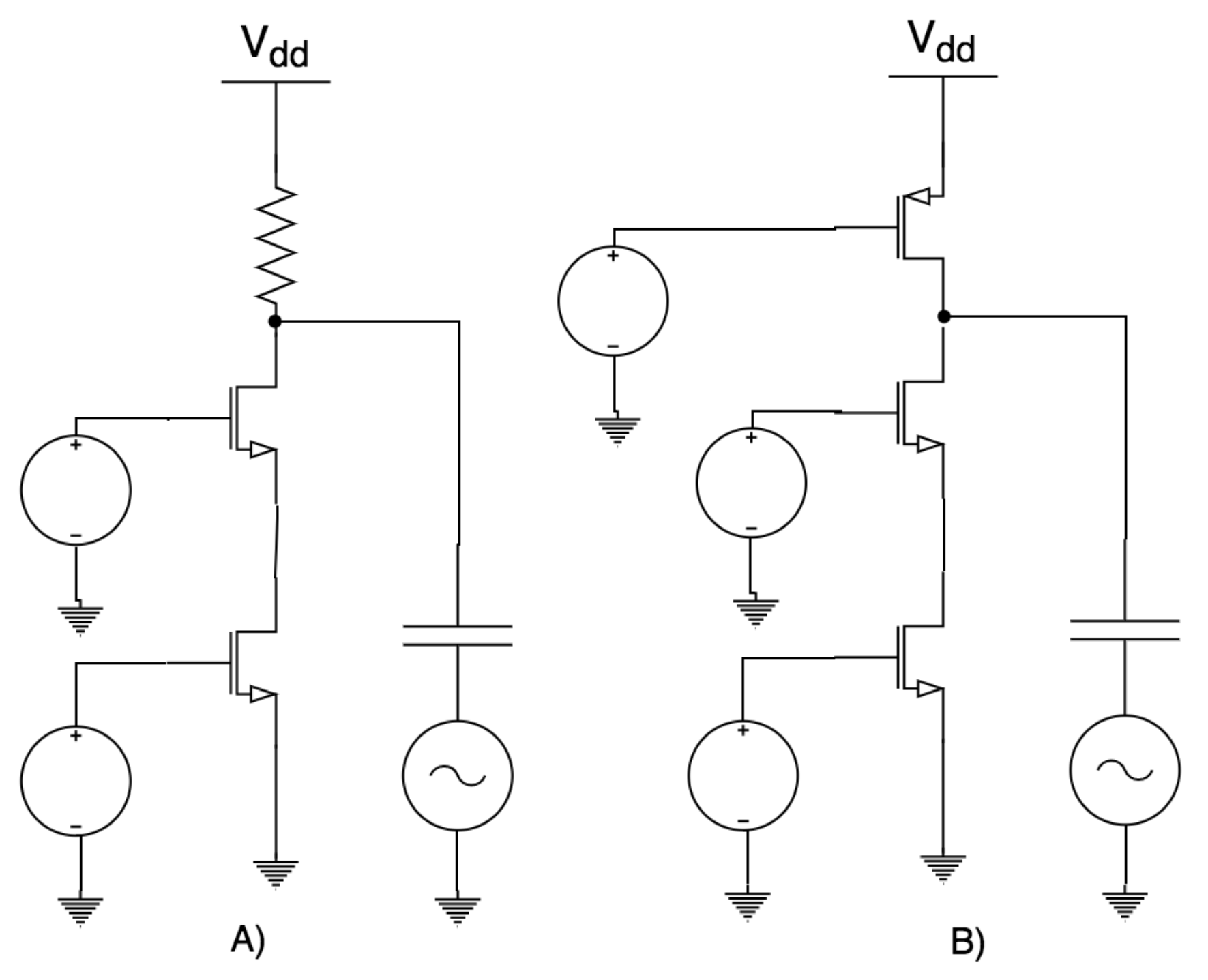
To reproduce the EMI pollution coming from the PCB, or from a generic ground plane or from close high-frequencies signal traces, an ideal sinusoidal voltage source is connected to the output pin of the generic amplifier, by means of an ideal capacitor, representing the capacitive coupling. A few picofarad forms a realistic value of the parasitic capacitance between a middle length trace and the PCB ground plane, as stated in [21,22,23]. The amplifiers are designed in a standard CMOS technology (the UMC 180nm) and the simulations are performed using the software Virtuoso, developed by Cadence, and, in particular, the Analog Design Environment (ADE) tool. In this way, the investigation of the EMI effect can be carried out with the biggest flexibility. Indeed, the sizing of the transistors can be easy changed, all the possible configuration of the amplifier can be simulated and the effect of the amplitude and the frequency of the interferences can be easy checked. The experimental measurements offer more eminent and complete results, but in this technology the simulations and the measurements of susceptibility fit rather well, Ref. [18,20,24]. Moreover, the simulations (if well supported by the transistor models) are a powerful instrument to understand the possible reasons of the suscepetibility. They indeed allow changing the conditions, the sizing, the settings, and so on..., and allow analyzing the effect of every change individually. Here, a list of the amplifier stages subjected to the interferences is briefly depicted. The DC and AC parameters and the transistors sizing are summarized in the following tables. The details on the circuit architectures, the schematics and the behavior of the amplifiers when subjected to the EMI are, instead, discussed in the corresponding sections. Table 1 refers to the common source stage shown in Figure 9; Table 2 summarizes the parameters of the common drain stage shown in Figure 10; in Table 3 the parameters of the cascode stage shown in Figure 11 are listed.

3. Susceptibility of the Common Source Stage

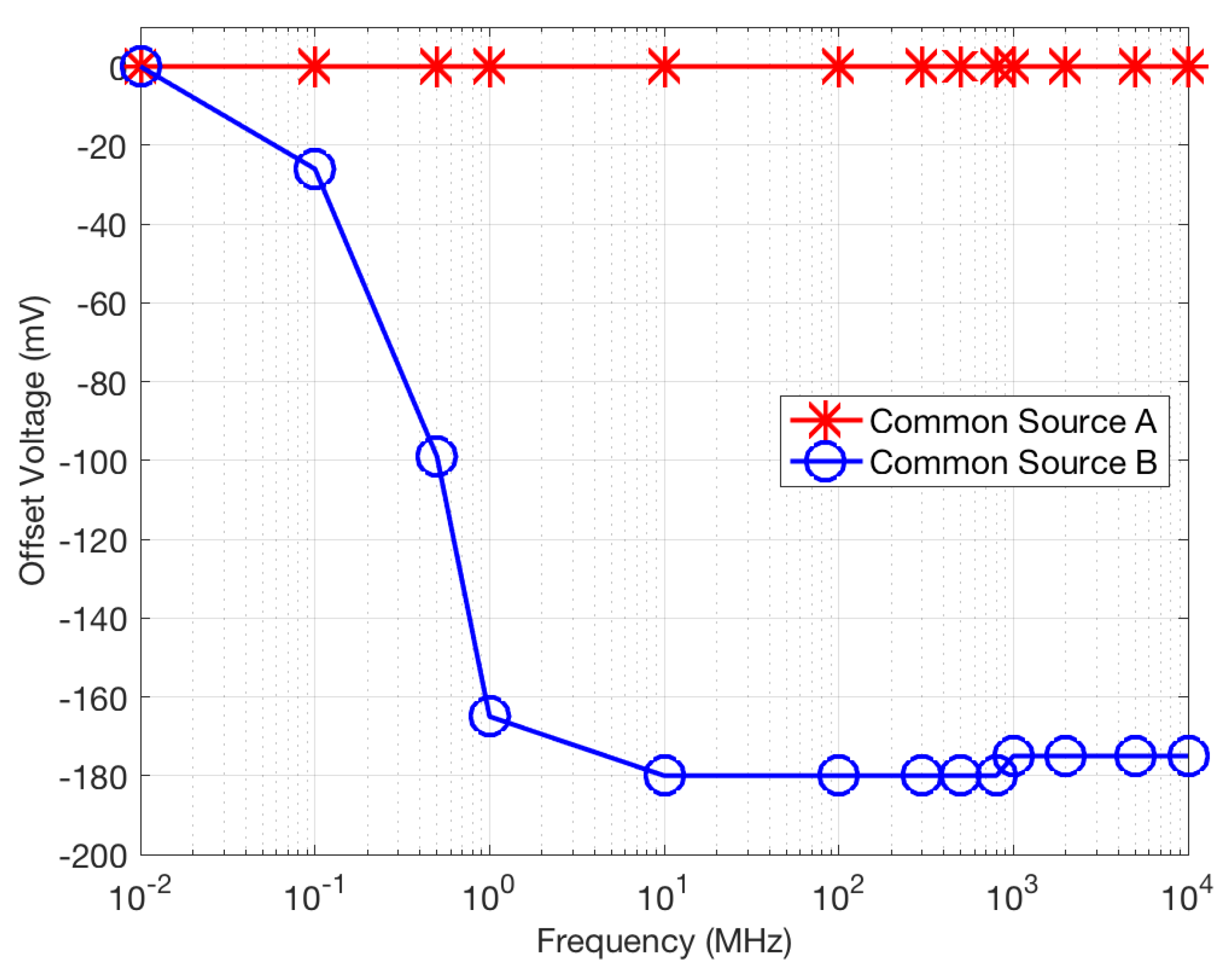
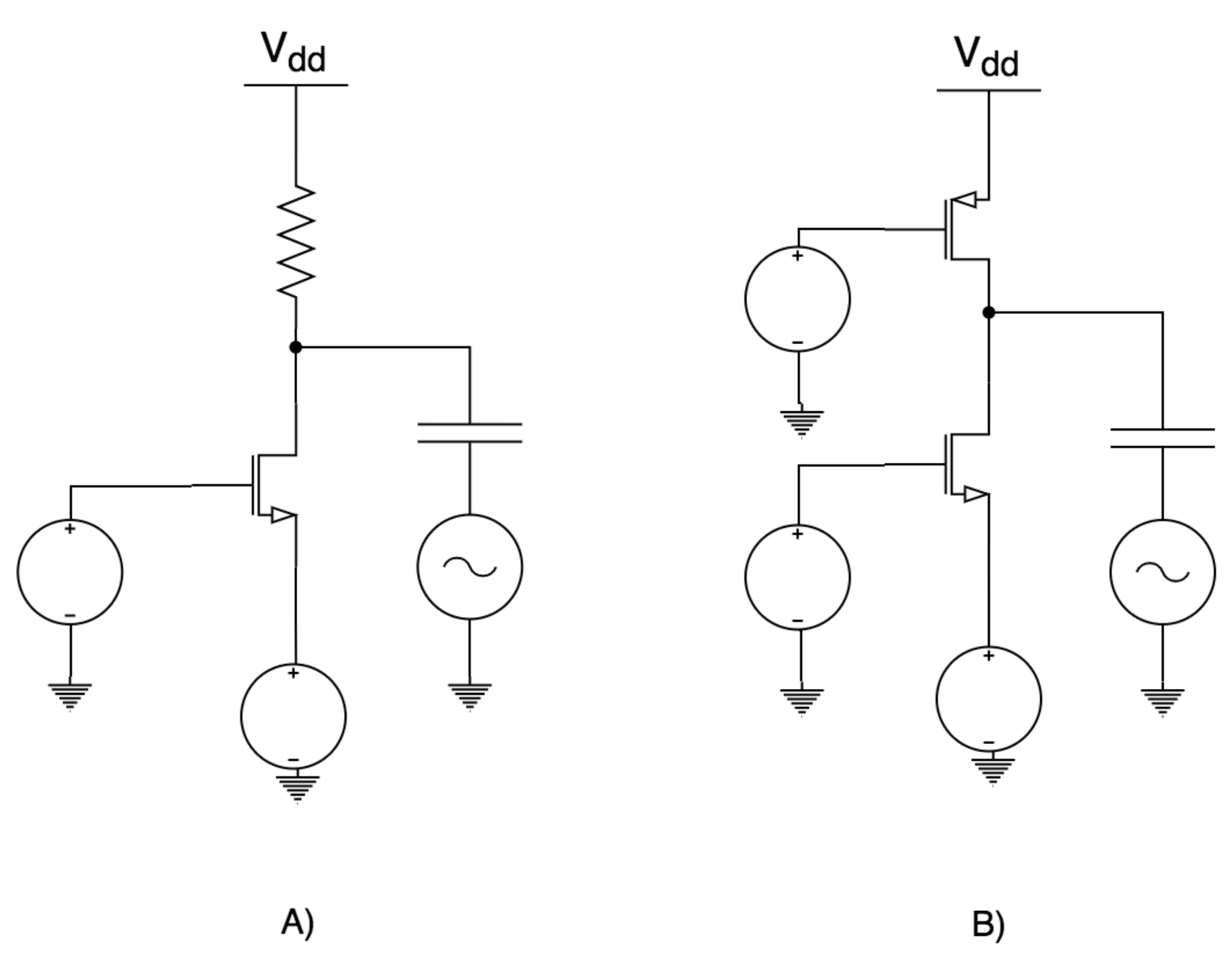
As a first step, a common source stage (CS) is investigated. The CS amplifier is based on a NMOS transistor, designed in the standard CMOS UMC (United Microelectronics Corporation) 180 nm technology; it is a N_18_MM device (which means regular threshold transistor for 1.8 V nominal voltage supply), with aspect ratio 20, length 1 μ m and width 20 μ m. The biasing point of the device is given by an ideal voltage source of 500 mV at the transistor gate and a resistor of 10 k Ω connected between the drain and the Vdd (1.8 V), as shown in Figure 9A. The resistor acts also as the active load of the CS stage. With the threshold of 374 mV, the biasing point sets the current at 57 μ A and these small signal parameters: gm 690 μ S and gds 7.2 μ S. As a single stage amplifier it exhibits a gain of 16 dB, a cut-off frequency of 1.5 MHz and a gain bandwidth product (GBW) of 11 MHz. The interference is represented by means of a sinusoidal signal with large amplitude and medium-large frequency. In particular, the amplitude is 1 V peak to peak and the frequency is ranging between 10 kHz and 10 GHz. The capacitive coupling versus the noisy ground plane is set to 1 pF. In this case, the comomon source amplifier exhibits a very low EMI induced offset (a few mV at maximum) and therefore a high immunity to the interferences coupled to the output pin. If a PMOS transistor takes the place of the resistor, as active load, the immunity changes. The new schematic is shown in Figure 9B. The resistive load has been substituted by an active load made of a PMOS transistor in saturation region, with the same aspect ratio of the NMOS counterpart. The gate of the PMOS is biased at 1V and the threshold voltage is around 500 mV. The operating point is slightly different to that of the first circuit and the current is now 54 μ A. The small signal simulations show a gain of 35 dB, a cut-off frequency of 180 kHz and a GBW of 10 MHz.
In this second case (with active load), the common source stage presents a large susceptibility to the interferences coupled to its output pin. Indeed, the EMI induced offset on the output voltage reaches about 200 mV and it is rather large in a wide frequency range, starting from 500 kHz (offset is 100 mV) up to 10 GHz. The results of the simulations performed on both the amplifiers are shown in Figure 12. If the amplitude of interfering signal increases, the induced offset has a large raise, as expected. For example, if the EMI amplitude is 1 V, the maximum offset becomes 400 mV.

4. Susceptibility of the Common Gate Stage

The behavior of the common gate stage (shown in Figure 13) is exactly the same of the common source stage. This is because the injection point (the drain of the transistor) is the same.

5. Susceptibility of the Common Drain Stage

The behavior of the common drain stage is now investigated. The first case is the schematic shown in Figure 10A, with the resistive load.
The NMOS device is a regular threshold transistor, with aspect ratio 20, length 1 μ m and width 20 μ m. The biasing point of the device is given by an ideal voltage source of 1.2 V at the transistor gate and a resistor of 10 k Ω connected between the source and gnd acts as a passive load. In this operating point the small signal parameters are: gm 763 μ S and gds 8.2 μ S. The current is 68 μ A and the threshold voltage is 379 mV. The AC gain is −1 dB and the cut-off frequency is 13 MHz. The second case is the common drain with the active load (as in Figure 10B). The input transistor is biased at the same 1.2 V, while the active load NMOS is biased by an ideal voltage source of 0.5 V connected to its gate. The operating point is slightly different from that of case A: the current is now indeed 50 μ A. The small signal parameters of the input transistor are now: gm 635 μ S and gds 6.8 μ S. The active load NMOS has similar parameters: gm of 633 μ S and gds of 7.1 μ S. The AC gain is 0 dB and the cut-off frequency is 9.6 MHz. To evaluate the susceptibility of the common drain stage the interferences are coupled to the transistor source (which is the output pin in this configuration) by means of a 1 pF capacitor. The EMI amplitude is 1 V peak to peak and the frequency is ranging between 10 kHz and 10 GHz. The results of the simulations performed on both the amplifiers are shown in Figure 14. As one can see both the schematics (A and B, with resistive or active load) are rather susceptible to the interferences, starting from a few MHz of the interfering signal frequency.

6. Susceptibility of the Cascode Stage

To have a complete overview of the single stage susceptibility, a cascode stage (common source + common gate) is also considered. The schematic is shown in Figure 11 with passive resistive load (A) and with active load (B). The transistors have always a length of 1 μ m and a width of 20 μ m. The common source transistor is biased with 0.5 V at the gate, while the common gate has a biased of 1V. The PMOS transistor in the schematic B is biased at 1.015 V in order to have operating points very similar between the circuits A and B, with the same current of about 50 μ A and the same small signal parameters. In particular, the common source transistor has: gm 633 μ S and gds 7.1 μ S. The common gate transistor has: gm 633 μ S and gds 7.4 μ S. Finally, the active load PMOS transistor has: gm 301 μ S and gds 3.5 μ S. In the first case (schematic A), the AC gain is 16 dB, the cut-off frequency is 1.5 MHz and the GBW is around 10 MHz. In the second case (schematic B), the AC gain is 45 dB, the cut-off frequency is 0.6 MHz and the GBW is around 10 MHz. The behavior of the cascode stage seems very similar to that of the common source stage. The circuit with passive load presents a negligible EMI-induced offset, while the circuit with active load is rather susceptible. The results of the simulations performed on both the amplifiers are shown in Figure 15.

7. Susceptibility of a Two Stages Amplifier

The next step is to investigate the susceptibility of a two stages differential input single ended amplifier. Therefore, a Miller amplifier has been considered. The Miller amplifier is indeed one of the most common CMOS OpAmp. It is based on a differential input stage with single ended conversion which has a behavior similar to that of a common source stage. The second gain stage is usually a common source plus an active load. Sometimes, depending on the applications, a voltage buffer is added after the second stage, to have a low output impedance.

7.1. Susceptibility of a Two Stages Amplifier in Open Loop Configuration

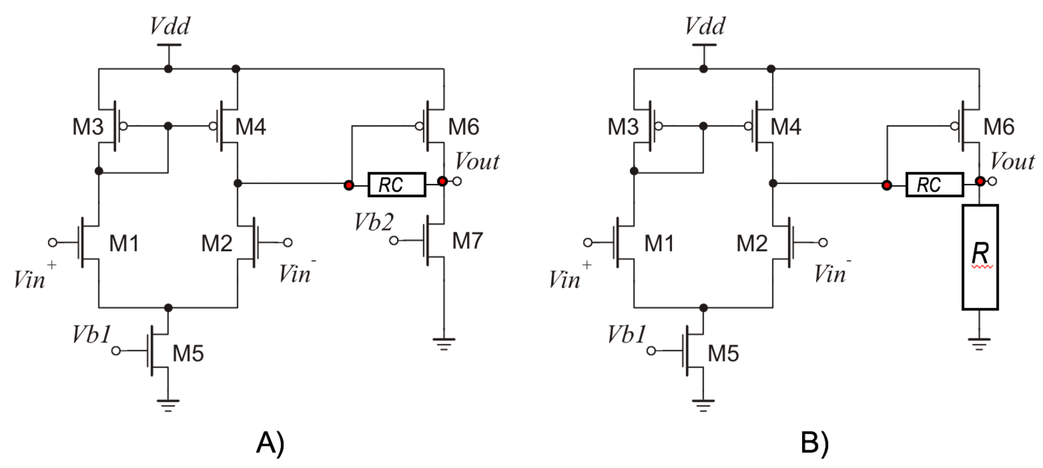
In this subsection, we consider a two stages amplifier in an open loop. This is usually the case of an amplifier used as a comparator. The schematics of the circuits are shown in Figure 16. On the left (Figure A) there is the amplifier with a resistive load, while on the right (Figure B) there is the same amplifier with active load. Concerning the A circuit, the AC simulations show a gain of 55 dB, a cut-off frequency of 22 kHz, a GBW of 12 MHz. Regarding the B circuit, the gain is 72 dB (thanks to the active load), the cut-off frequency is 2.8 kHz and the GBW is 12 MHz. Although both the circuits are now used in an open loop configuration, they have a frequency compensation RC network that ensures 75 of phase margins if the circuits are in a closed loop. The main small signal parameters and the operating point are also listed in Table 4.
The offset induced by the interfering signals capacitively coupled to the output pin is shown in Figure 17: the blue line represents the Miller amplifier with active load (A circuit in Figure 16) and the red one represents the amplifier with the passive load (B circuit in Figure 16). The output stage of the amplifier in the open loop configuration is exactly a common source stage and a similar EMI susceptibility could be expected. Instead, as shown by the simulation results plotted in Figure 17, the EMI induced offset has two main differences. The first one is the susceptibility of the amplifier with passive load: although it is much less than the amplifier with active load, it is rather high, much higher than the susceptibility of the simple common source stage with passive load (which is negligible). The maximum offset is indeed 600 mV and the critical frequencies range from tens of MHz up to Ghz. The second difference is that the susceptibility of the amplifier with active low decreases at very high frequencies. It does not happen in the simple stages (common source, gate, drain and cascode).
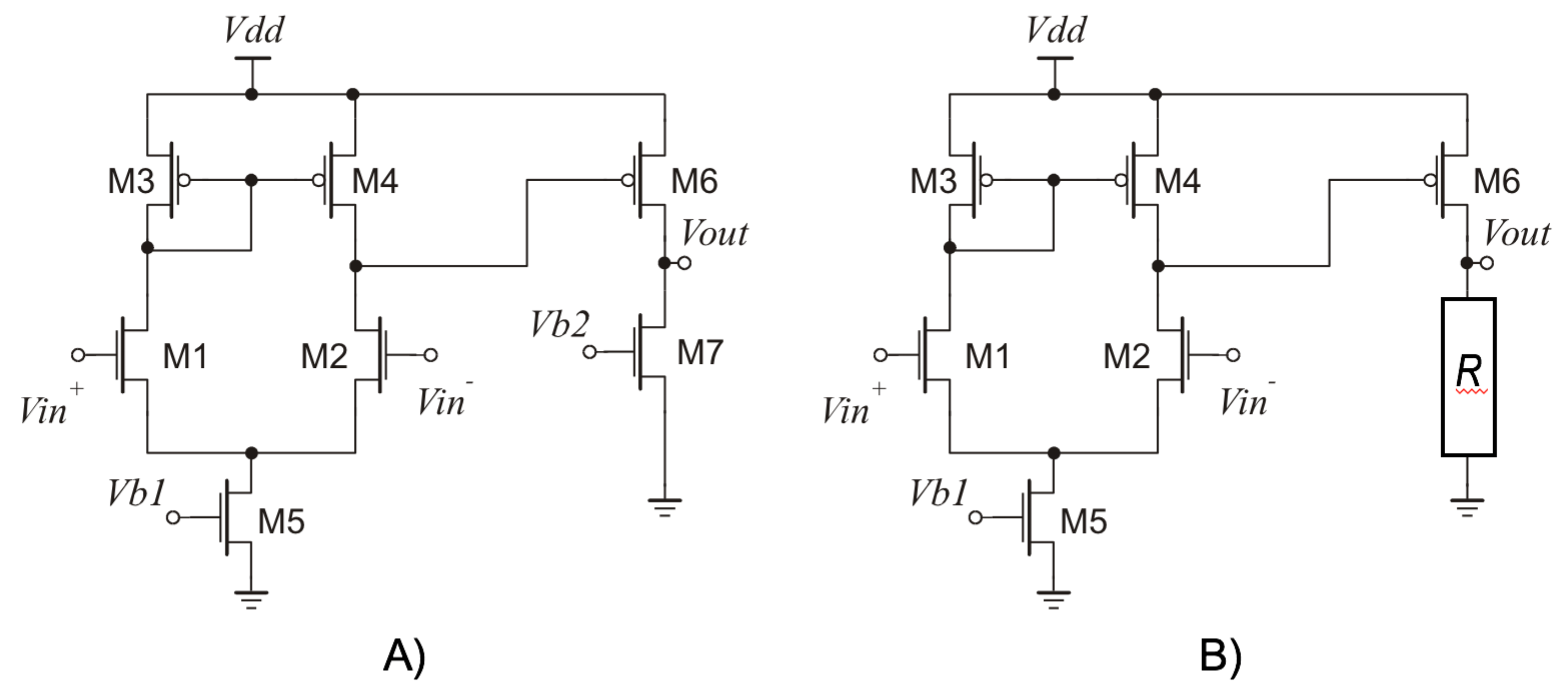
Finally, another huge difference is the value of the offset, which is much larger than that of the single stage: indeed, the maximum offset is above 1 V in the Miller amplifier, while it is less than 200 mV in the common source stage. One of the possible reason of the different behavior could be the RC network for the frequency compensation. It is indeed in the amplifier schematic, even if it is used in an open loop. The sizing of the RC network is: 3 k Ω for the resistor and 1 pF for the capacitor. The RC network is directly connected to the output pin, it is across the first and the second stage and it may cause a typical phenomenon, Ref. [25,26,27], called EMI charge pumping, which leads to a severe DC shift of the biasing point. To investigate this, a schematic without the RC network (see Figure 18) has been simulated and the simulation results are plotted in Figure 19.
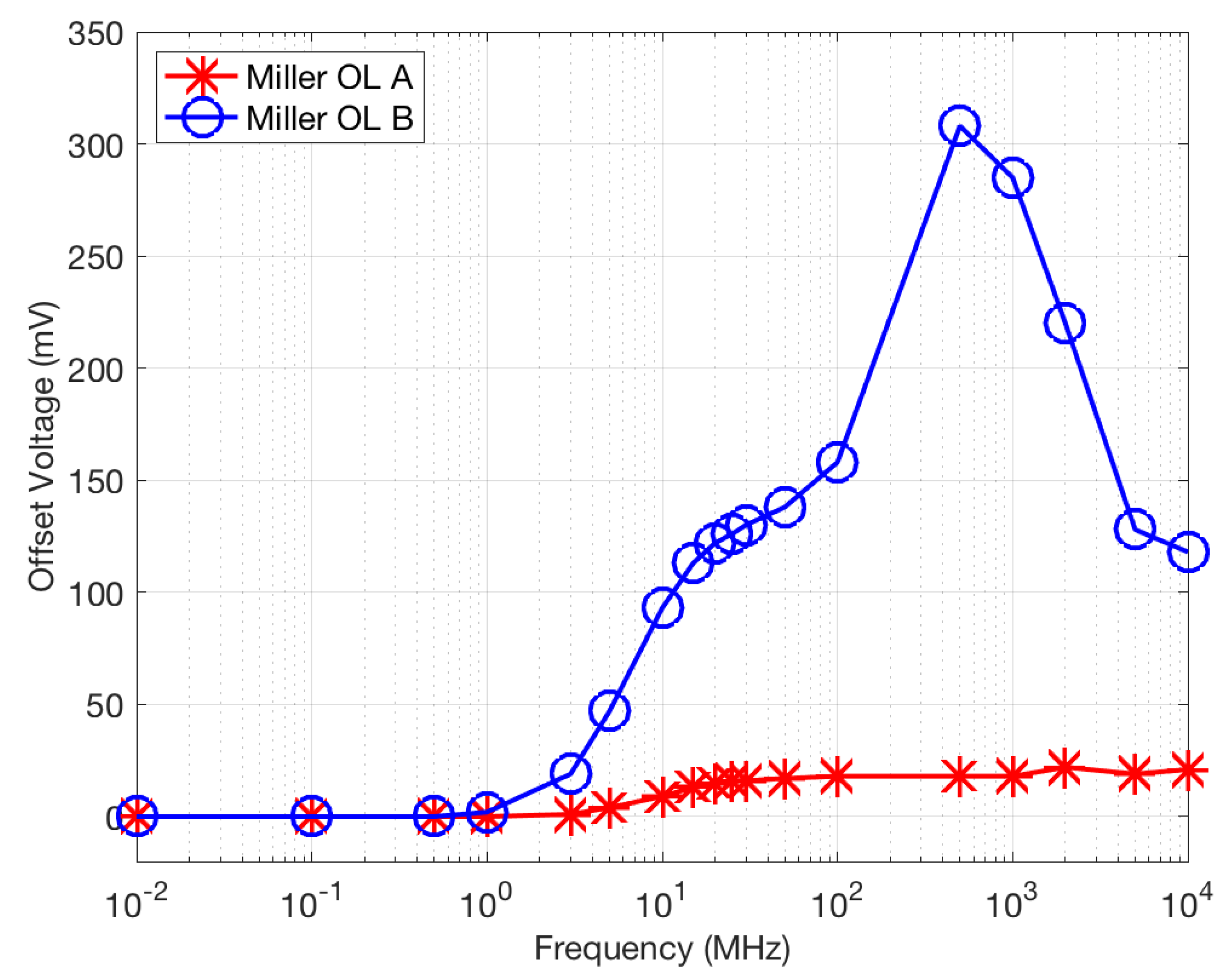
By comparing Figure 17 and Figure 19, it results that: the EMI induced offset is much reduced, and it is almost negligible in the case of resistive load (B circuit). On the other hand, there are still some differences which can be due to the first stage of the amplifier, which polarizes the second stage and is also weakly connected to the ouput node by means of the parasitics.

7.2. Susceptibility of a Two Stages Amplifier in Closed Loop Configuration

The circuits shown in Figure 16 are now connected in a closed loop and the effect of interferences are investigated. The feedback loop decreases the output impedance and a reduction of the EMI induced offset is reasonably expected. The results are indeed plotted in Figure 20.
The susceptibility is similar to that of a simple common source stage (the maximum EMI induced offset is the same); the behavior of the amplifier with the active load is very similar to that of the amplifier with resistive load and the range of uncritical frequencies is enlarged up to a few hundreds of MHz.

8. Overview of the Obtained Results

The exact repercussion of electromagnetic interference, which is injected into arbitrary pins of an integrated amplifier, is very hard to predict owing to the fact that all the existing coupling paths need to be taken into account.
The investigation of single stage amplifier, such as common source, common gate, common drain and cascode, is easier, but non trivial. The susceptibility can be related, indeed, to the output impedance. The common source, common gate and cascode stage have a high impedance output node and it is known that the high impedance (floating) node are more prone to pick up the noise. The behavior of the common drain stage is less intuitive, but it can be still attributed to the impedance: at large frequencies the output impedance of the common drain (which is small at low frequencies) grows up. Moreover, the parasitic gate-source capacitance of the common drain creates a feedback from the output to the input and the charge pumping is maximum. This explains the increasing of the EMI induced offset above the hundreds of MHz.
Regarding the two stages amplifier, a distinction must be done between the open loop and closed loop configuration. For the closed loop configuration, it results that the Miller amplifier (independently on the passive or active low) has a negligible offset until 100 MHz. This result is reasonable because the feedback reduces the output impedance and therefore the susceptibility. Moreover, in this case, by choosing one of the several architectures depicted in the literature, with a high immunity to the EMI injected into the input pin [8,9,10,13,14,15,16], the susceptibility to the output pin can be further reduced, ref. [20]. For the open loop configuration, the behavior is rather unpredictable, but it does not depend on the transistor sizing because a common source stage with the same size and biasing has a different behavior (similar to the one depicted in Section 3). By removing the RC network, the EMI-induced offset assumes more reasonable values. Therefore, a possible cause of the very large offset at the middle high frequencies can be found by comparing the output node with and without the frequency compensation network. We found that the RC decreases the impedance seen from the drain of the PMOS transistor, making it similar to that of the passive load. In brief, the output node could be in a kind of tri-state. An additional voltage buffer could be useful in this case to reduce the output impedance and therefore the susceptibility. The results obtained in the open loop configuration can be also exemplary to understand the behavior of several circuits, such as digital ones and logic gates. Finally, a general consideration is that the behavior at very high frequencies is always difficult to predict. Neither the measurements are so determining, because of the parasitics of the IC package which complicate the analysis.

9. Conclusions

This paper compares the susceptibility to the interferences coupled to the output pin in several different topologies, starting from the single stage amplifiers up to the whole operational Miller amplifier. The output pin is indeed a critical point of injection and therefore effort and attention must be spent to understand the coupling mechanism. The investigation of single stage amplifiers, such as common source, common gate, common drain and cascode, is easier, but non trivial. The susceptibility can be related, indeed, to the output impedance. Regarding the two stages amplifier, similar considerations can be drawn but also a distinction must be done between the open loop and closed loop configuration. In general, the open loop configuration exhibit a larger and less predictable EMI induced offset, while the amplifier with the feedback loop shows a good immunity up to hundreds of MHz.

Author Contributions

All the authors have contributed substantially to the paper. A.R. has provided the simulation tools and has written the paper; L.C. and Z.K.-V. have written the paper and supervised the work. All authors have read and agreed to the published version of the manuscript.

Funding

This research received no external funding.

Conflicts of Interest

The authors declare no conflict of interest.

References

  1. Van De Beek, S.; Leferink, F. Robustness of a TETRA Base Station Receiver Against Intentional EMI. IEEE Trans. Electromag. Compat. 2015, 57, 461–469. [Google Scholar] [CrossRef]
  2. Dawson, J.F.; Flintoft, I.D.; Kortoci, P.; Dawson, L.; Marvin, A.C.; Robinson, M.P.; Stojilovic, M.; Rubinstein, M.; Menssen, B.; Garbe, H.; et al. A Cost-Efficient System for Detecting an Intentional Electromagnetic Interference (IEMI) attack. In Proceedings of the IEEE International Symposium on Electromagnetic Compatibility, Gothenburg, Sweden, 1–4 September 2014; pp. 1252–1256. [Google Scholar]
  3. IEEE Draft Recommended. Practice for Protecting Public Accessible Computer Systems from Intentional EMI. In Practice for Protecting Public Accessible Computer Systems from Intentional EMI; IEEE P1642/D10; IEEE: Piscataway, NJ, USA, 2014; pp. 1–31. [Google Scholar]
  4. Kune, D.F.; Backes, J.; Clark, S.S.; Kramer, D.; Reynolds, M.; Fu, K.; Kim, Y.; Xu, W. Ghost Talk: Mitigating EMI Signal Injection Attacks against Analog Sensors. In Proceedings of the 2013 IEEE Symposium on Security and Privacy, Berkeley, CA, USA, 19–22 May 2013; pp. 145–159. [Google Scholar]
  5. Van De Beek, S.; Leferink, F. Current intentional EMI studies in Europe with a focus on STRUCTURES. In Proceedings of the IEEE International Symposium on Electromagnetic Compatibility Tokyo 2014, Tokyo, Japan, 12–16 May 2014; pp. 402–405. [Google Scholar]
  6. Fiori, F.; Crovetti, P. Prediction of high-power EMI effects in CMOS operational amplifiers. IEEE Trans. Electromagn. Compat. 2006, 48, 153–160. [Google Scholar] [CrossRef]
  7. Ramdani, M.; Sicard, E.; Boyer, A.; Ben Dhia, S.; Whalen, J.J.; Hubing, T.H.; Coenen, M.; Wada, O. The Electromagnetic Compatibility of Integrated Circuits-Past, Present and Future. IEEE Trans. Electromagn. Compat. 2009, 51, 78–100. [Google Scholar] [CrossRef]
  8. Crovetti, P.S. Operational amplifier immune to EMI with no baseband performance degradation. Electr. Lett. 2010, 46, 209–210. [Google Scholar] [CrossRef]
  9. Walravens, C.; Van Winckel, S.; Redoute, J.M.; Steyaert, M. Efficient reduction of electromagnetic interference effects in operational amplifiers. Electr. Lett. 2007, 43, 84–85. [Google Scholar] [CrossRef]
  10. Richelli, A. CMOS OpAmp resisting to large electromagnetic interferences. IEEE Trans. Electromagn. Compat. 2010, 52, 1062–1065. [Google Scholar] [CrossRef] [Green Version]
  11. Fiori, F. EMI susceptibility: The achilles’ heel of smart power ICs. IEEE EMC Mag. 2015, 4, 101–105. [Google Scholar] [CrossRef]
  12. Crovetti, P.; Musolino, F. Interference of Spread-Spectrum EMI and Digital Data Links under Narrowband Resonant Coupling. Electronics 2020, 9, 60. [Google Scholar] [CrossRef] [Green Version]
  13. Richelli, A.; Matig-a, G.; Redoute, J.M. Design of a folded cascode opamp with increased immunity to conducted electromagnetic interference in 0.18 μm CMOS. Microelectr. Reliab. 2015, 55, 654–661. [Google Scholar] [CrossRef]
  14. Redoute, J.M.; Steyaert, M. EMI-Resistant CMOS Differential Input Stages. IEEE Trans. Circuits Syst. I Regul. Pap. 2010, 57, 323–331. [Google Scholar] [CrossRef]
  15. Richelli, A. Increasing EMI immunity in novel low-voltage CMOS OpAmps. IEEE Trans. Electromagn. Compat. 2010, 54, 947–950. [Google Scholar] [CrossRef] [Green Version]
  16. Sbaraini, S.; Richelli, A.; Kovács-Vajna, Z.M. EMI susceptibility in bulk-driven Miller opamp. Electr. Lett. 2010, 46, 1111–1113. [Google Scholar] [CrossRef]
  17. Redouté, J.-M.; Steyaert, M. An EMI Resisting LIN Driver in 0.35-micron High-Voltage CMOS. IEEE J. Solid State Circuits 2007, 42, 1574–1582. [Google Scholar] [CrossRef]
  18. Richelli, A.; Delaini, G.; Grassi, M.; Redouté, J.-M. Susceptibility of Operational Amplifiers to Conducted EMI Injected Through the Ground Plane into Their Output Terminal. IEEE Trans. Reliab. 2016, 65, 1369–1379. [Google Scholar] [CrossRef]
  19. Richelli, A.; Colalongo, L.; Toninelli, L.; Rusu, I.; Redouté, J.-M. Measurements of EMI susceptibility of precision voltage references. In Proceedings of the EMCCompo 2017, St. Petersburg, Russia, 4–8 July 2017. [Google Scholar]
  20. Becchetti, S.; Richelli, A.; Colalongo, L.; Kovács-Vajna, Z.M. A Comprehensive Comparison of EMI Immunity in CMOS Amplifier Topologies. Electronics 2019, 8, 1181. [Google Scholar] [CrossRef] [Green Version]
  21. Preibisch, J.B.; Duan, X.; Schuster, C. An Efficient Analysis of Power/Ground Planes With Inhomogeneous Substrates Using the Contour Integral Method. IEEE Trans. Electromagn. Compatib. 2014, 56, 980–989. [Google Scholar] [CrossRef]
  22. Kachout, M.; Bel Hadj Tahar, J.; Choubani, F. Modeling of Microstrip and PCB Traces to Enhance Crosstalk Reduction. In Proceedings of the IEEE SIBIRCON-2010, Listvyanka, Russia, 11–15 July 2010; pp. 594–597. [Google Scholar]
  23. Ricchiuti, V. Evaluation of the Effective Electrical Parameters of a PCB Trace for Accurate Signal Integrity Simulations. In Proceedings of the PIERS 2004, Pisa, Italy, 28–31 March 2004; pp. 77–80. [Google Scholar]
  24. Richelli, A.; Kennedy, S.; Redouté, J.M. An EMI-Resistant Common-Mode Cancelation Differential Input Stage in UMC 180 nm CMOS. IEEE Trans. Electromagn. Compatib. 2017, 59, 2049–2051. [Google Scholar] [CrossRef]
  25. Redouté, J.-M.; Steyaert, M. EMC of Analog Integrated Circuits; Springer: Dordrecht, The Netherlands, 2010. [Google Scholar]
  26. Richelli, A.; Redouté, J.-M. A Methodological Approach to EMI Resistant Analog Integrated Circuit Design. IEEE EMC Mag. 2015, 4, 92–100. [Google Scholar]
  27. Redouté, J.-M.; Steyaert, M. Current mirror structure insensitive to conducted EMI. IET Electr. Lett. 2005, 41, 1145–1146. [Google Scholar] [CrossRef] [Green Version]
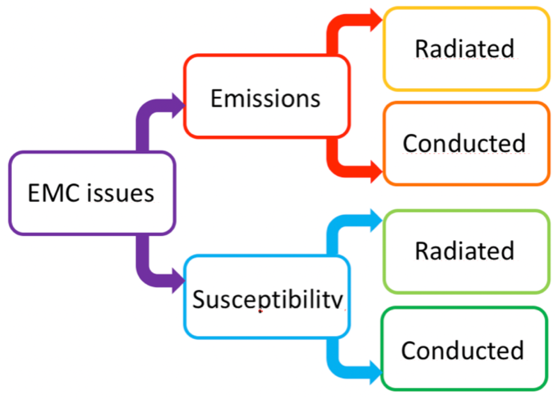
Figure 1. EMC issues.
Electronics 09 00304 g001
Figure 2. Possible coupling mechanisms for EMI attack.
Electronics 09 00304 g002
Figure 3. EMI induced offset in ua741: interferences coupled to the output pin.
Electronics 09 00304 g003
Figure 4. EMI induced offset in OPA705: interferences coupled to the output pin.
Electronics 09 00304 g004
Figure 5. EMI induced offset in NE5534: interferences coupled to the output pin.
Electronics 09 00304 g005
Figure 6. EMI induced offset in ICL7611: interferences coupled to the output pin.
Electronics 09 00304 g006
Figure 7. EMI induced offset in series voltage references: interferences coupled to the output pin.
Electronics 09 00304 g007
Figure 8. EMI induced offset in shunt voltage references: interferences coupled to the output pin.
Electronics 09 00304 g008
Figure 9. Schematics of the common source stage, with passive (A) and active (B) load respectively.
Electronics 09 00304 g009
Figure 10. Schematics of the common drain stage, with passive (A) and active (B) load respectively.
Electronics 09 00304 g010
Figure 11. Schematics of the cascode stage, with passive (A) and active (B) load respectively.
Electronics 09 00304 g011
Figure 12. EMI induced offset in the common source stage.
Electronics 09 00304 g012
Figure 13. Schematics of the common gate stage, with passive (A) and active (B) load respectively.
Electronics 09 00304 g013
Figure 14. EMI induced offset in the common drain stage.
Electronics 09 00304 g014
Figure 15. EMI induced offset in the cascode stage.
Electronics 09 00304 g015
Figure 16. Schematic ofthe Miller amplifier: (A) with active load, (B) with resistive load.
Electronics 09 00304 g016
Figure 17. EMI induced offset in the Miller amplifier, open loop configuration.
Electronics 09 00304 g017
Figure 18. Schematic ofthe Miller amplifier without the RC network for the frequency compensation: (A) with active load, (B) with resistive load.
Electronics 09 00304 g018
Figure 19. EMI induced offset in the Miller amplifier without RC network, open loop configuration.
Electronics 09 00304 g019
Figure 20. EMI induced offset in the Miller amplifier with RC network, closed loop configuration.
Electronics 09 00304 g020
Table 1. DC and AC parameters and Transistor Sizing of the Common Source Stage.
DC Biasing and AC ParametersComponents Sizing
Common Source with RVbiasN = 500 mV, 16 dB gainW = 20 μ m, L = 1 μ m
(passive load)1.5 MHz cut-off freq., 11 MHz GBWR = 10 k Ω
Common Source with PMOSVbiasN = 500 mV, VbiasP = 1 V, 35 dB gainWn = 20 μ m, Ln = 1 μ m
(active load)180 kHz cut-off freq., 10 MHz GBWWp = 20 μ m, Lp = 1 μ m
Table 2. DC and AC parameters and Transistor Sizing of the Common Drain Stage.
DC Biasing and AC ParametersComponents Sizing
Common Drain with RVbiasN = 1.2 V, −1dB gainW = 20 μ m, L = 1 μ m
(passive load)13 MHz cut-off freq.R = 10 k Ω
Common Drain with NMOSVbiasN = 1.2 and VbiasN2 = 500 mV, 0 dB gainWn = 20 μ m, Ln = 1 μ m
(active load)9.6 MHz cut-off freq.Wn2 = 20 μ m, Ln2 = 1 μ m
Table 3. DC and AC parameters and Transistor Sizing of the Cascode Stage.
DC Biasing and AC ParametersComponents Sizing
Cascode with RVbiasN1 = 0.5 V, VbiasN2 = 1 V, 16 dB gainWn1,2 = 20 μ m, Ln1,2 = 1 μ m
(passive load)1.5 MHz cut-off freq., 10 MHz GBWR = 10 k Ω
Common Drain with NMOSVbiasN1 = 0.5 V, VbiasN2 = 1 V, VbiasP = 1.015 VWn1,2 = 20 μ m, Ln1,2 = 1 μ m
(active load)45 dB gain, 0.6 MHz cut-off freq., 10 MHz GBWWp = 20 μ m, Lp = 1 μ m
Table 4. DC and AC parameters and Transistor Sizing of the Two Stages Amplifier.
DC Biasing and AC ParametersComponents Sizing
Miller with R (passive load)Vb1 = 1.16 V, 55 dB gainWn1,2 = 20 μ m, Ln1,2 = 1 μ m;
Wp3,4,6 = 25  μ m, Lp3,4,6 = 0.5 μ m
22 kHz cut-off freq., 12 MHz GBWWn5 = 20 μ m, Ln5 = 1 μ m; R = 10 k Ω
Miller with NMOS (active load)Vb1 = Vb2 = 1.16 V,Wn1,2 = 20 μ m, Ln1,2 = 1 μ m;
Wp3,4,6 = 25  μ m, Lp3,4,6 = 0.5 μ m
72 dB gain, 2.8 kHz cut-off freq., 12 MHz GBWWn5 = 20 μ m, Ln5 = 1 μ m; Wn7 = 8.5  μ m, Ln7 = 0.5 μ m