1. Introduction
Integrated circuit (IC) package design is a complex and time-consuming process for achieving a reliable and high-performance system. It requires the multidisciplinary optimization of multiple design variables associated with thermomechanical and electrical characteristics. In thermomechanical design, various parameters, such as the materials and thicknesses of an epoxy molding compound and the adhesive for die attachment, must be considered in IC-package analysis. The analysis objective is to minimize the package warpage and avoid delamination, thus ensuring structural reliability and manufacturing process availability. To perform the analysis, numerical techniques, e.g., the finite-element modeling of an IC package, can be employed, which require large amounts of computational resources and simulation time.
In the electrical design of an IC package, numerous design variables, including the geometric parameters of the signal interconnects and power-delivery networks, must be considered for achieving the high throughputs, bandwidths, and data rates of the devices in the package. The electrical characteristics of an IC package are determined using computationally expensive simulations involving the finite-element method (FEM), the finite-difference time-domain (FDTD) method, and the method of moments.
A difficulty in IC-package design is that the results of the electrical and thermomechanical designs are affected by each other, as they share common design variables, necessitating a tradeoff design. To efficiently obtain an optimized solution for both designs, a multiphysics simulation scheme is preferred; however, such a scheme is not suitable for the development of practical applications [
1,
2]. During industrial developments of an IC package, thermomechanical and electrical engineers separately perform simulations and analyses for their own goals and iteratively modify their designs by communicating with each other. It is time-consuming to optimize a tradeoff design, because both the electrical and thermomechanical characteristics are predicted via computationally expensive methods.
Additionally, the package types are continuously evolving into complex multichip packages such as the embedded multimedia card, the embedded multichip package, and universal flash storage. From the viewpoint of electrical design, these package types significantly increase the difficulty of IC-package design, because they employ high-density ICs vertically and horizontally stacked in the package substrate, as well as differential interconnects of SERDES devices for high-speed IC communications. In particular, high-speed interconnect design is one of the crucial parts of real IC-package design, which is the focus of this study. The reason why it is critical is that the use of high-speed interconnect in the state-of-the-art IC package dramatically increases; however, its analysis and optimization method become more difficult and less efficient [
3,
4,
5].
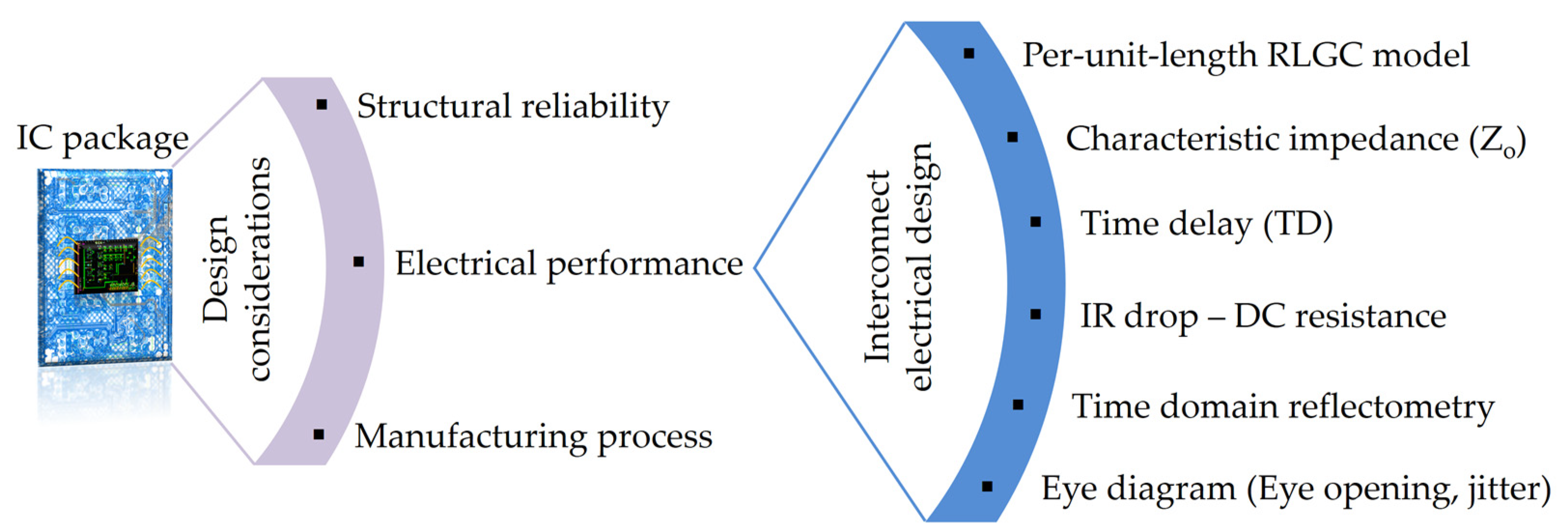
As the data rate and density of the IC-package interconnect increase, the effects of parasitics such as mutual capacitance, mutual inductance, and the skin effect cannot be ignored. In the simulation, a broadband interconnect model must be adopted to successfully capture the high-frequency effect of parasitics and accurately analyze various electrical characteristics, as shown in
Figure 1. Full-wave simulation techniques using the FEM and the FDTD method are effective for practical design. They provide a convenient method for the analysis of an arbitrary interconnect structure in the wideband frequency range. In [
6,
7,
8], the previous approach was used to successfully extract scattering parameters and estimate the signal integrity characteristics of an IC-package interconnect. However, even with the advantages of the high design flexibility and accurate results, this approach has the practical problem of being time-consuming. To obtain accurate results using the full-wave simulation of the entire IC-package interconnect, a large number of analysis meshes are inevitably generated, which leads to an extremely long simulation time for one design case. Moreover, the high complexity of a multichip package significantly increases the numbers of geometric parameters and degrees of freedom in the electrical design. Consequently, the solution space is substantially expanded. It requires a large amount of time to complete an examination of all design cases and obtain an optimized solution using conventional design methods. It is difficult to achieve the timely completion of the IC-package design using the conventional methods for the electrical design of an IC package [
9,
10].
In this paper, an efficient method for the reduction of a solution space and the optimization of the electrical design of an IC package using design of experiments (DoE) and the domain decomposition method (DDM) is presented [
11,
12,
13,
14,
15]. For rapid analysis, the number of degrees of freedom is reduced according to the DoE results, and the analysis domain is decomposed into subdomains. A recombined impedance matrix for the subdomain solutions is analytically derived.
2. Methods
The proposed approach is intended to facilitate the development of the high-speed interconnect for practical IC packages. For the rapid and efficient design and analysis of the electrical characteristics of the IC-package interconnect, the proposed method adopts two approaches: reducing the number of degrees of freedom in the IC-package design and reducing the maximum number of computational meshes generated during a full-wave simulation. The reduction of the number of degrees of freedom in the IC-package interconnect design is achieved by determining a critical variable (CV) of the interconnect design via the Taguchi method, which employs an orthogonal array to efficiently reduce the number of test sets required in a design procedure [
16]. The computational mesh number is reduced by applying the DDM to the IC-package interconnect and deriving a closed-form expression for the recombination impedance parameters, which is simply converted into the scattering parameters (S-parameters) and characteristic impedance (Z
o). The proposed approach is a hybrid method that involves identifying the critical design variables and dividing the IC-package interconnect into segmented parts, i.e., the CV-based DDM (CVDDM).
The proposed CVDDM mainly comprises two parts—CV analysis and the CV-based DDM—as shown in
Figure 2 [
11,
12,
13,
17,
18]. In the CV analysis, a strategy using DoE based on the Taguchi method is employed. The design variables of the IC-package interconnect are discriminated between low and high sensitivities to electrical characteristics such as Z
o, the RLGC parameters, and the S parameters. The objective of the CV analysis step is determining the CVs, which significantly affect the electrical characteristics of the IC-package interconnect. Since the solution space for the electrical design of a recent IC-package interconnect is extremely large when all the geometric parameters are considered, CV-based design is easier than the previous approach that involves a full factorial test of the IC-package interconnect and the evaluation of all combinations of design variables in a full-wave simulation.
2.1. CV Analysis
The first step in the CV analysis is the generation of an orthogonal array (OA) considering the numbers and levels of all geometric parameters in the complete IC-package interconnect. To reduce the number of simulations and efficiently determine the CVs, a fractional factorial characteristic based on the Taguchi method is adopted rather than a full factorial approach. In statistics, the optimized result using OAs and the Taguchi method is close to that of the full factorial approach. The existence and construction of OAs are introduced in [
16]. The notation OA (N, q, s, t) is adopted, which represents a matrix of N rows and q columns with entries from S. N and q represent the numbers of simulation runs and design parameters, respectively. S is a set of the levels of the design variables, and t represents the strength, as described in [
16]. To appropriately select an OA, an existing database for OAs can be used [
19]. A useful property of OAs is that a subarray with N rows and k columns extracted from an OA (N, q, s, t) can be an OA (N, k, s, u) whose u is equal to the minimum value between k and t. Thus, a new OA (N, k, s, u) is simply obtained by discarding one or more columns of an OA (N, q, s, t) found in the database when a number of parameters of j smaller than k is needed in the IC-package interconnect design.
The next step of the CV analysis is extracting the electrical characteristics of a complete IC-package interconnect represented as an RLGC model, which can be reduced to an LC model with the assumption of a lossless transmission line. All LC models corresponding to simulation runs of OA (N, k, s, u) are obtained. The technique of S parameter-based transmission-line characterization [
20] is employed to extract the LC models from the S parameters of complete IC-package interconnects. Each S-parameter result is acquired using a full-wave simulation based on the FEM. In this study, an IC-package interconnect based on differential transmission lines is characterized, because such interconnects have been widely adopted in recent high-speed packages. Through a full-wave simulation of differential transmission lines, the results for S parameters with four ports and a single-ended configuration are extracted. These are converted into mixed-mode S parameters [
21] to construct an LC model of a coupled line. The LC model of a coupled line consists of self-inductances (L
11, L
22), self-capacitances (C
11, C
22), mutual inductances (L
12, L
21), and mutual capacitances (C
12, C
21). These parameters are obtained from the mixed-mode S parameters via S-parameter-based RLGC extraction [
20]. The even and odd-mode propagation constants (γ
e, γ
o) are given as follows:
where S
dd and S
cc represent the differential-mode and common-mode submatrices, respectively, of the mixed-mode S parameters.
The closed-form expressions for even and odd-mode characteristic impedances (Z
oe, Z
oo) are derived as follows [
22]:
where Z
oe,ref and Z
oo,ref represent the reference impedances for even and odd-mode propagations, respectively.
Finally, the LC model is extracted as follows:
It is worth noting that the proposed method is limited to a lossless package interconnect. To extend the method to a lossy package interconnect including R and G components, we will verify it in a further study. The effects of the design variables on the L and C values are examined using a sensitivity analysis based on the Taguchi method. The L and C variations of all the simulation runs corresponding to OA (N, k, s, u) are calculated. The design variables (i.e., V
1, V
2, …, V
k) for each case of L
11, L
12, C
11, and C
12 are ranked according to the sensitivity. A design variable where a larger variation is observed is assigned higher priority. Thus, the priority order of the design variables is established for each L and C value. For instance, a line width represented as V
i may significantly affect L
11, L
12, and C
11, whereas its effect on C
12 may be smaller. Then, the line width V
i has a small priority-order number for L
11, L
12, and C
11 and a large priority-order number for C
12. Hence, all the design variables have four numbers indicating the priority order for L
11, L
12, C
11, and C
12. The priority-order numbers of V
i for L
11, L
12, C
11, and C
12 are denoted as P
i,L11, P
i,L12, P
i,C11, and P
i,C12, respectively. A linear combination of the priority numbers for V
i is given as follows:
where w
L11, w
L12, w
C11, and w
C12 represent the weights, which are equal to 1 in this study. However, the values can be adjusted for other design objectives. For instance, w
L12 and w
C12 are more significant than w
L11 and w
C11 when crosstalk reduction is a primary goal of an IC-package interconnect design. The CVs for the high-speed IC-package interconnect design are determined according to the linear combination of the priority numbers. The CVs are selected among the design variables for which the result of the linear combination is smaller than a specific number.
2.2. CV-Based DDM
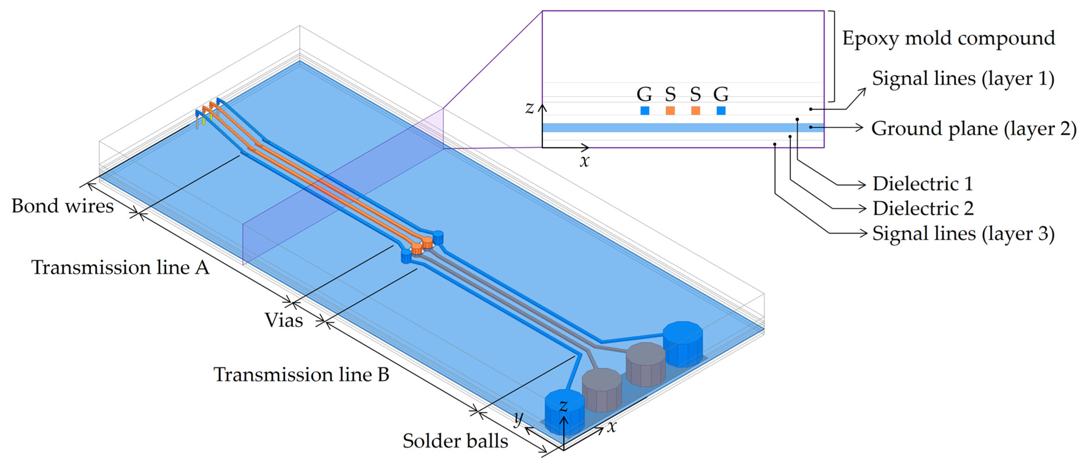
In this subsection, a DDM for a high-speed IC-package interconnect is presented to reduce the number of analysis meshes handled during a single simulation run. In the DDM, the analysis domain of the original and complete package interconnect is decomposed into nonoverlapping subdomains. The solutions of the adjacent subdomains are related by the continuity conditions at the interfaces. In this study, on the basis of the geometry, the original domain of the IC-package interconnect is divided into several subdomains corresponding to bonding wires, transmission lines, vias, and solder balls, as shown in
Figure 3. The subdomains are nonoverlapping, and the current–continuity relationship is valid at their interfaces. Intersegment coupling is not considered in this DDM, for the simplicity of the design and analysis.
For the bonding-wire segment, four coplanar bonding wires (ground–signal–signal–ground (G-S-S-G) configuration) are commonly employed [
23,
24,
25]. Its shape follows the JEDEC 4-point. A transmission-line segment can consist of various types of transmission lines, such as a microstrip, coplanar waveguide, and conductor-backed coplanar waveguide lines. A via has a stacked structure and is employed for layer transition. A solder-ball segment connects the signal and power nets of an IC package to those of printed circuit boards. Its shape is modeled as a polygonal column rather than a sphere for the simplicity of the analysis. The polygonal column model successfully captures the capacitive effect of a solder ball, which significantly affects the electrical characteristics of the entire IC-package interconnect.
Next, the impedance parameters of all the segments with nominal values of the design variables are determined using full-wave simulations. Since an interconnect structure is partitioned into small segments, full-wave simulations for the segments are more efficient than the analysis of the entire structure with large meshes. Additionally, by sweeping the CVs, more impedance parameters of the segments (including the various values of the CVs) can be determined, allowing an electrical design engineer to easily explore the solution space of an IC-package interconnect and obtain a tradeoff solution.
An analytical method to recombine the impedance parameters of subdomains is developed to rapidly and systematically obtain the original impedance parameter of a complete IC-package interconnect. The signaling-type IC-package interconnect, which is the focus of the present study, performs differential signaling with five conductors. The segments of the IC-package interconnect comprise four narrow conductors with the configuration of G-S-S-G, which are located on a wide conductor. Since all the ground conductors are regarded as a return path in the complete IC-package interconnect, the electrical performance of the entire IC-package interconnect can be completely characterized using a four-port impedance parameter. However, the segments of the decomposed IC-package interconnect require the impedance parameters containing more ports. The narrow conductors of the segments at the decomposition interface are considered as the microstrip lines or striplines to examine the CV effect. Hence, the bonding-wire and solder-ball segments contain six ports, whereas the transmission-line and via segments have eight ports.
Figure 4 presents the block diagram for deriving analytical expressions for a recombination impedance parameter. Suppose that
ZC(i,j) is the impedance parameter of the original interconnect and that
ZA(i) and
ZB(j) are those of the segments where the original interconnect is decomposed. The indices
i and
j represent the order of the impedance parameter sets when the segments A and B contain the results obtained by sweeping the various values of the CVs. As explained previously,
ZA(i) and
ZB(j) can be easily determined using full-wave simulations. The objective of the recombination step is to express
ZC(i,j) using
ZA(i) and
ZB(j). Here, the notation
is defined as the recombination operation. Moreover, the external and internal ports are defined as the port of the original interconnect and the port at the interface generated by the DDM, respectively. The external port
and internal ports
and
are shown in
Figure 5. Then, the impedance parameter
ZC is given as follows [
26]:
where
Zmn,A (m, n = 1, 2, …, 6) and Zmn,B (m, n = 1, 2, …, 8) are the entities of the impedance parameters ZA and ZB, respectively.
The specific impedance parameter associated with the differential interconnect of the IC package is analytically derived. Even though the impedance parameters of the DDM segments can be completely recombined using computer-aided engineering tools such as ANSYS Electronics Desktop and Keysight Advanced Design Systems, the proposed method based on the analytical expressions has the advantages of rapid estimation and systematic automation based on script-level programming, which is not dedicated to particular languages. Thus, the development of the IC-package interconnect can be more flexible.
In the final step of the CV-based DDM, the impedance parameter is converted into the S-parameter
SC as follows:
where
Zo represents a reference impedance value, which is nominally 50 Ω.
E represents the identity matrix.
Then, a mixed-mode S-parameter is given as follows [
27]:
3. Results and Discussion
The proposed CVDDM for the electrical design of the IC-package interconnect was demonstrated using a full-wave simulation of a basic structure of a differential interconnect. We adopt the ANSYS HFSS software for a full-wave simulation.
Figure 5 shows the simple structure and the stacked layers of the IC-package interconnect, which included bond wires, transmission lines, vias, and solder balls. The simulation model comprised three conductor layers. Copper was used as the conductor material. Dielectrics 1 and 2 were placed above and below the ground plane on layer 2, respectively. The nominal values of the dielectric constant and loss tangent were 4.3 and 0.009, respectively. An epoxy mold compound (EMC) was placed on dielectric 1 for package protection. The dielectric constant and loss tangent of the EMC were 4.1 and 0.022, respectively.
Before the proposed CVDDM was applied, the design variables of the IC-package interconnect were defined, as shown in
Figure 6. The bond-wire segment heights, length, diameter, and spacing were represented as h
bw1, h
bw2, L
bw, w
bw, and s
bw, respectively. From a practical viewpoint, it is preferred that the electrical characteristics of the bond-wire segment are adjusted using the length variable L
bw. This variable may be a CV, while the other variables use nominal values. For the transmission-line segment, d
TL, s
TL, w
TL, and h
TL represent the length, spacing, and width of the signal line and the distance between the signal line and the ground plane, respectively. ε
r represents the dielectric constant. For the via segment, d
v, s
v, and h
v represent the diameter, spacing, and length of the via, respectively. w
t represents the width of the transition part from a via to a transmission line. L
v represents the total length of the via segment, including the transition part. Commonly, via designs using the variables h
v and L
v are not flexible in the practical IC-package process. For the solder-ball segment, d
sb, s
sb, and h
sb represent the diameter, spacing, and height of the solder ball, respectively. w
t represents the width of the transition part. L
sb represents the total length of the solder-ball segment. Nominally, w
t is equivalent to the width of the transmission line.
To demonstrate the proposed CVDDM for the basic structure of the IC-package interconnect, the design variables and their levels were determined considering the package manufacturing process. Eleven variables were employed: d
bw, d
TL, s
TL, w
TL, h
TL, ε
r, d
v, s
v, d
sb, h
sb, and s
sb. Their levels were varied from 50% to 150% of the nominal value (i.e., level 2), as shown in
Table 1. The non-included variables in the CV list were h
bw1, h
bw2, w
bw, s
bw, L
v, L
sb, and w
t. The default values of h
bw1, h
bw2, w
bw, s
bw, L
v, and L
sb were 50, 110, 25, 40, 310, and 530 μm, respectively. The w
t value was equivalent to w
TL for each simulation run. Using these variables, the Taguchi method was applied to the complete IC-package interconnect. An OA, i.e., OA (27, 11, 3, 2), was generated [
19], as shown in
Table 2. The OA had 27 rows and 11 columns. The rows represent the 27 distinct experiments to conduct a FEM-based simulation of the entire IC-package interconnect.
As described in the previous section, the self-inductance, mutual inductance, and capacitances for all the experiments were extracted using the S parameters obtained via the FEM simulations and the S-parameter-based RLGC extraction method, as shown in
Table 2. The self-inductance L
11 varied from 1.63 to 3.41 nH, and the L
12 values were between 0.33 and 1.06 nH. Moreover, the FEM simulation results indicated that the self-capacitance C
11 ranged from 0.70 to 1.91 pF, and the mutual capacitance C
12 ranged from 0.11 to 0.27 pF. According to these results, a DoE analysis was performed, as shown in
Figure 7. The effects of all the design variables on the electrical characteristics of the complete IC-package interconnect were clearly revealed using the Taguchi method. Additionally, the priority-order numbers of all the variables for the L
11, L
12, C
11, and C
12 effects were obtained, as shown in
Table 3. When the linear combination of the priority-order numbers (i.e., P
i) was estimated,
wL11,
wL12,
wC11, and
wC12 were all set to 1. According to the P
i values, five variables (d
bw, d
TL, s
TL, w
TL, and h
TL) were selected as CVs. Thus, the bond-wire length and transmission-line design significantly affected the overall electrical characteristics of the complete IC-package interconnect. The nominal designs of the vias and solder balls were considered to be less important.
In this study, the limit value of Pi was empirically determined. A number between 22 and 24 was selected as the limit value of Pi, so that we had only five CVs, for design simplicity. A rigorous study for determining Pi depending on the application of the IC-package interconnect was not conducted. Future research can be performed to identify more effective Pi values; the use of the limit number of Pi is desirable for the systematic approach, which enables design optimization and automation employing a new method such as a machine-learning technique.
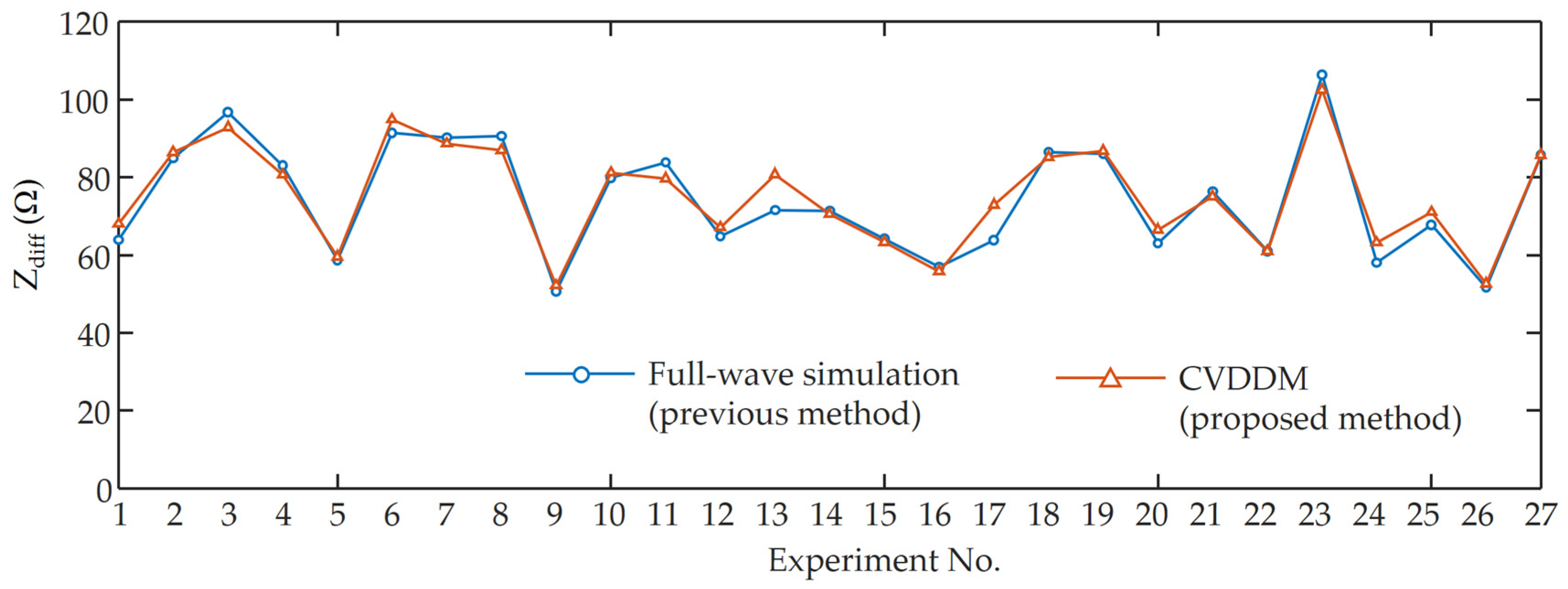
Finally, numerous datasets containing the impedance parameters of the DDM segment were obtained by sweeping the CVs in the range of interest. By applying the recombination technique to the datasets, the electrical characteristics of the IC-package interconnect were rapidly determined for various cases. Before beginning the design based on the CVDDM, it will be verified via comparison with the full-wave simulation results of the complete interconnect structure. Since the differential characteristic impedance (Z
diff) of the IC-package interconnect is a good metric to evaluate the interconnect performance in a simple manner, the Z
diff for the proposed CVDDM was compared with the result of a full-wave simulation of a complete IC-package interconnect, as shown in
Figure 8. The differential characteristic impedances for the 27 cases shown in
Table 2 were compared. As shown in
Figure 8, the proposed CVDDM exhibited good agreement with the full-wave simulation of the entire IC-package interconnect. Although there were discrepancies in the Z
diff values for a few cases, they were insignificant considering practical use in the early design stage. The discrepancy is caused by ignoring intersegment coupling.
The proposed CVDDM produces a design space providing direct insight into the signal integrity of the high-speed IC-package interconnect. It allows a package design engineer to rapidly and efficiently optimize an IC-package interconnect and easily develop a new package solution. For instance, a design space with the CVs w
TL and h
TL is shown in
Figure 9. The figure presents all the Z
diff values of the full IC-package interconnect for various cases of interest when the development of a new package. Suppose that the thermal and mechanical group provides two possible choices of the dimensions associated with A (h
TL = 30 μm, w
TL = 10 μm) and B (h
TL = 10 μm, w
TL = 30 μm). An immediate response can be achieved using the design space constructed via the CVDDM. As shown in
Figure 10, the S-parameter results for A and B were significantly different. The dimensions of A must be selected to ensure the good electrical characteristics of the IC-package interconnect. When the previous method involving full-wave simulation is used, the computation time is long, and the proper decision cannot be made. We compare the total amount of simulation time between the previous full-wave simulation method and the proposed CVDDM for the cases A and B shown in
Figure 9. The simulation times of the previous and the proposed methods are 2761 seconds and 1470 seconds, respectively. The simulation time is substantially reduced up to 46.7%. Even though the reduced time is 1291 seconds, this is only considering two cases. In a real design process, there are so many cases of interest. Thereby, the time difference between the previous and proposed methods is too much larger. The time evaluation is summarized as shown in
Table 4 in the revised manuscript.


