Article

Influence of Flexibility of the Interconnects on the Dynamic Bending Reliability of Flexible Hybrid Electronics

1
Fraunhofer EMFT Research Institution for Microsystems and Solid State Technologies, 80686 Munich, Germany
2
Institute of Electronic Packaging Technology, Technische Universität Dresden, 01069 Dresden, Germany
*
Author to whom correspondence should be addressed.
Electronics 2020, 9(2), 238; https://doi.org/10.3390/electronics9020238
Submission received: 28 December 2019 / Revised: 13 January 2020 / Accepted: 22 January 2020 / Published: 1 February 2020
(This article belongs to the Special Issue Flexible/Stretchable Electronics)

Abstract

:
The growing interest towards thinner and conformable electronic systems has attracted significant attention towards flexible hybrid electronics (FHE). Thin chip-foil packages fabricated by integrating ultra-thin monocrystalline silicon integrated circuits (ICs) on/in flexible foils have the potential to deliver high performance electrical functionalities at very low power requirements while being mechanically flexible. However, only very limited information is available regarding the fatigue or dynamic bending reliability of such chip-foil packages. This paper reports a series of experiments where the influence of the type of metal constituting the interconnects on the foil substrates on their dynamic bending reliability has been analyzed. The test results show that chip-foil packages with interconnects fabricated from a highly flexible metal like gold endure the repeated bending tests better than chip-foil packages with stiffer interconnects fabricated from copper or aluminum. We conclude that further analysis work in this field will lead to new technical concepts and designs for reliable foil based electronics.

1. Introduction

Recently developed process technologies for the integration of thin semiconductor components like state-of-the-art micro-controller ICs (integrated circuits) and sensor devices on or in flexible foil substrates have paved the way for extremely thin and even bendable electronic systems [1,2,3]. This so-called flexible hybrid electronics (FHE) enables a wide spectrum of new applications in consumer electronics, like for instance advanced wearable health monitoring devices such as smart watches and sensor plasters [4,5,6,7,8,9] and bendable as well as foldable mobile phones [10,11]. Besides, niche applications such as electronic skin for robotics as well as prosthetics [12,13,14,15] and ultra-thin IC packages [16,17,18] for miniaturized electronic packages could also benefit from FHE. Recent advances in FHE are very promising [19,20,21,22,23,24,25] and therefore, FHE is expected to play a vital role in further developments of these applications. Furthermore, low cost production of FHE components such as chip-foil packages for these applications could be achieved by implementing roll-to-roll (R2R) manufacturing processes [26]. A majority of the aforementioned applications require devices that are anticipated to bend repeatedly during the device usage, for, e.g., sensors and actuators placed in smart plasters and electronic skin. However, FHE is a relatively younger field of research that is still in its nascent stages of development and hence, information available regarding the static [27,28,29,30,31,32] as well as dynamic bending reliability [33,34,35,36] of FHE components is rather very limited. Several studies have shown that the failure of chip-foil packages during repeated bending occur mainly because of the cracking of interconnects rather than the delamination of the chip from foil or chip fracture [34,35,36]. Hence, it is crucial to investigate various factors influencing the dynamic bending reliability of interconnects and to devise techniques to enhance the dynamic bending reliability of chip-foil packages. It is well known that the flexibility of metals increase with a decrease in their Young’s modulus and increase in Poisson’s ratio [37,38,39,40]. However, quantification of the influence of flexibility of the interconnect metal on the dynamic bending reliability would serve as a key information for fabricating reliable FHE systems. In line with this objective, we investigated the effect of flexibility of interconnects on the dynamic bending reliability of chip-foil packages by conducting repeated bending tests on chip-foil packages having interconnects fabricated from three metals with varying flexibility namely (i) copper, (ii) aluminum and (iii) gold.
This paper is organized as follows. The ensuing Section 2 explains the sample fabrication process. Then, the experimental setup used for the investigations is described in the subsequent Section 3. Next, the following Section 4 discusses the obtained test results. Finally, concluding remarks and our outlook for future works are included in Section 5.

2. Sample Fabrication Process

The chip-foil package samples required for investigating the dynamic bending reliability were fabricated by following various process steps that can be grouped as follows: 1. Interconnect fabrication on the foil substrate, 2. thinning of the silicon chips and 3. integration of the ultra-thin silicon chips on the foil substrates.

2.1. Fabrication of Interconnects on the Foil Substrate

We implemented semiconductor microfabrication processes such as sputter deposition, lithography and wet etching for patterning the interconnects on the foil substrate. Commercially available UPILEX® 50S polyimide (PI) with a thickness of 50 µm was used as the substrate foil for fabricating the interconnects. UPILEX® 50S was selected as the substrate due to its lower high-temperature shrinkage, higher maximum operating temperature, higher glass transition temperature (Tg), lower permeability to gas and water vapor, lower moisture uptake and lower coefficient of thermal expansion (CTE) [41,42,43]. The process was performed on the wafer level and therefore the first step in the process was to attach the PI foil on a 6′′ carrier wafer. Next, the respective metals were sputter deposited on the PI foil using a Balzers LLS vertical sputter tool. The first step in the sputter deposition process was the activation of the substrate surface with argon plasma etching. Copper and gold exhibit poor adhesion to the polyimide foil. Therefore, a titanium tungsten (Ti10W90) adhesion layer having a thickness of 15 nm was sputter deposited prior to depositing copper and gold without breaking vacuum after deposition of the adhesion layer. After deposition of the metals, a positive photoresist (AZ®1514) was spin coated and then lithographically patterned to define the interconnects. Exposure was performed at a Süss mask aligner MA6 using soft contact. Then, wet etching of the metals was executed using commercially available etchants: K–KI based etchant for Au, Na2S2O8 solution for Cu and PWS etchant for Al. Etch rates were adjusted by using the appropriate concentration and temperature to achieve etch rates in the range of 180–270 nm/min. The TiW layer was then etched separately using H2O2. Finally, the resist was stripped using suitable solvent-based media to pattern the interconnects. The layer thickness of the fabricated interconnects was about 300 nm.

2.2. Fabrication and Thinning of Silicon Chips

The ultra-thin silicon chips consisting of daisy chain test patterns were fabricated following the well-known dicing-by-thinning process that follows a subtractive approach [44]. In the first step, daisy chain tests patterns were fabricated on prime silicon wafers having a thickness of approximately 700 µm. Then, grooves were scribed on the front side of the sample wafer using a wafer saw along the predefined boundaries of the test chips. After sawing, the sample wafer was bonded to a rigid carrier wafer using a solvable glue. Next, the bonded stack was transferred to a wafer grinder where the sample wafer was thinned down by grinding from its rear side using rotating diamond wheels that remove material physically. Wafer grinding normally consists of a coarse and a fine grinding step depending on the size of the diamonds used to remove material. The rear side of the wafer is typically rough even after fine grinding having total thickness variation (TTV) in the range of 1–2 µm. After completion of the grinding step, chemical mechanical polishing involving fine removal of wafer (<1 µm/min) with abrasive medium was performed to improve the surface quality of the rear side of the wafer thereby enhancing the fracture strength of the wafer [45]. Finally, the thinned down test chips were released from the carrier wafer by dissolving the glue with an organic solvent. The thickness of the released chips was about 20 µm. Further information about the dicing-by-thinning process is available in [44].

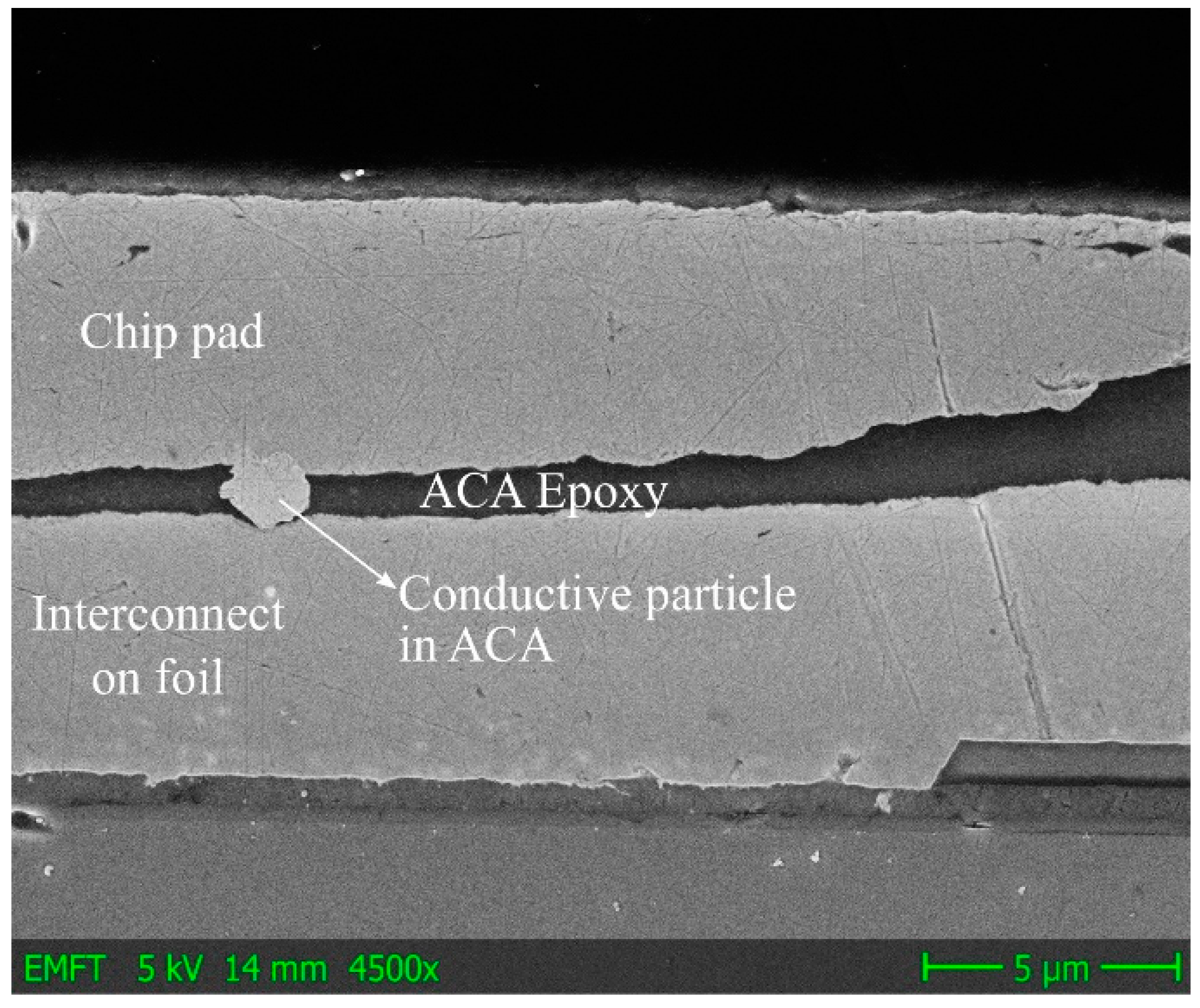
2.3. Integration of Ultra-Thin Silicon Chips on Foil Substrates

The fabricated ultra-thin silicon chips were then bonded on to the interconnects of the foil substrates using flip-chip bonding with an anisotropic conductive adhesive (ACA). ACA is an epoxy consisting of suspended metal particles that establishes electrical interconnection between the chip pads and the corresponding foil interconnect upon application of pressure. The salient feature of ACA is that it is conductive in the Z-axis while remaining non-conductive in the X and Y-axes upon curing. We used Delo Monopox AC 245 that has nickel particles having a diameter of 5.3 µm to bond the chips in this work [46]. The flip-chip bonding process was performed in a programmable die bonding equipment, Panasonic FCB3 at a temperature of ~200 °C and a bonding force of 5 N. Figure 1 presents a scanning electron microscopy image of a typical example of the cross-section of single contact pad interconnection of a flip-chip bonded chip-foil package. The fabricated chip-foil packages with copper, aluminum and gold interconnects are shown in Figure 2.

3. Experimental Setup and Procedure
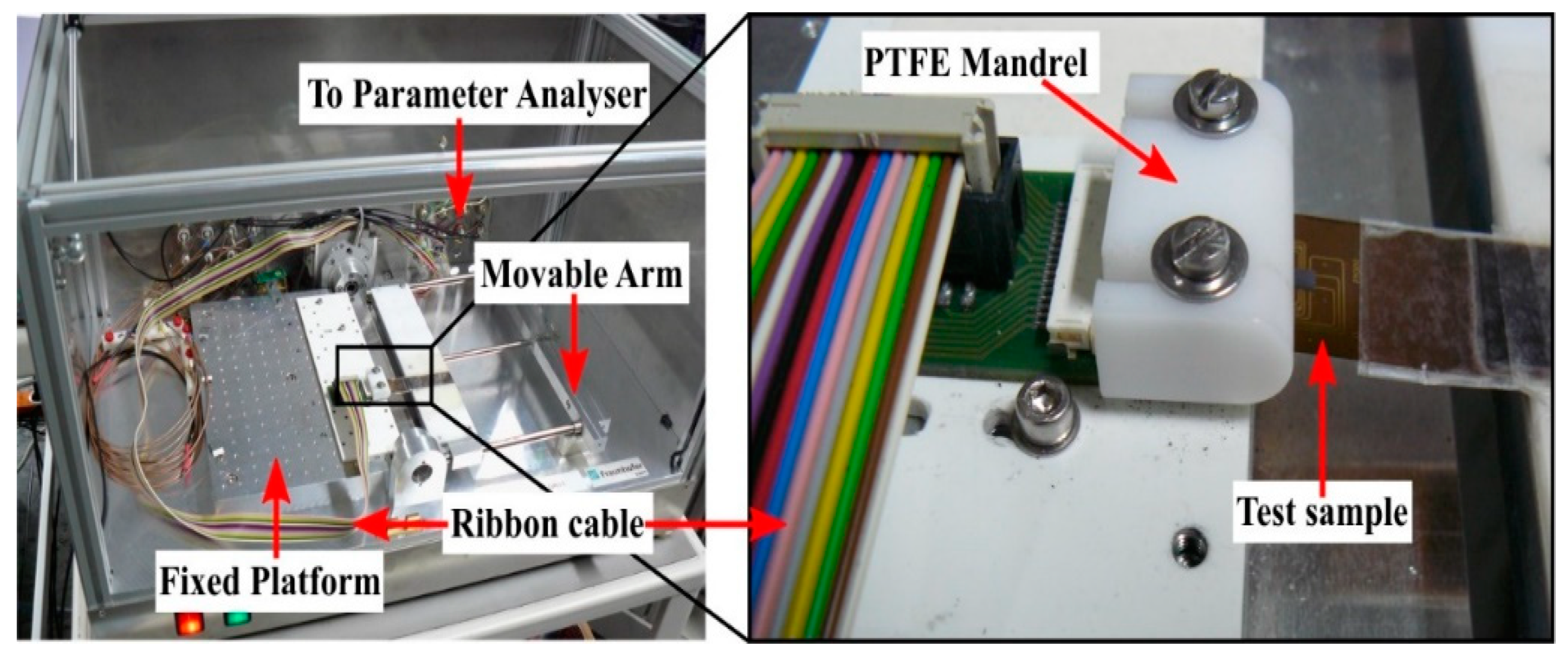
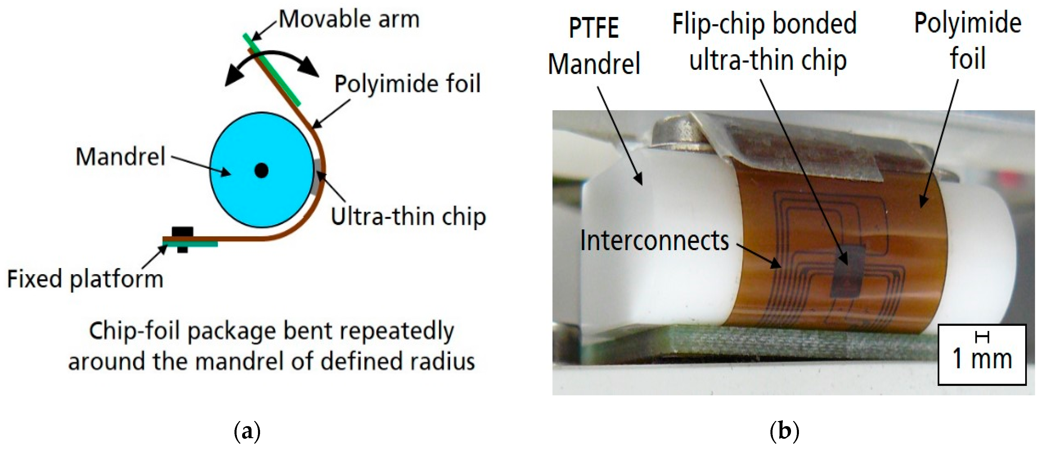
3.1. Test Equipment

The dynamic bending tests on the fabricated chip-foil packages were performed in custom-built test equipment (shown in Figure 3) that facilitates online measurement of the electrical characteristics of the test samples. The equipment primarily consists of two parts: 1. a fixed platform and 2. a movable arm. The samples were fixed to the test equipment with one end of the samples attached to the fixed platform and the other end to the movable arm. The chip-foil package sample was attached to the fixed platform through a zero-insertion force (ZIF) connector mounted on a Printed Circuit Board, PCB (Figure 4). The PCB connects the test samples with a parameter analyzer (Keysight 4156C) via a ribbon cable for measuring the electrical parameters of the samples. The resistance of daisy chain structures of the chip-foil package samples was measured during the tests in this work and a change in the daisy chain resistance was monitored to identify failure of the test samples. The movable arm was connected to a stepper motor from Festo AG & Co. KG (Esslingen, Germany) that controlled the bending cycles through a software interface. The number of bending cycles and the frequency of the bending cycles can be defined via the software interface. A polytetrafluoroethylene (PTFE) mandrel was attached to the fixed platform to define the bending radius and the samples were bent repeatedly back and forth around the mandrel during the tests.

3.2. Experimental Procedure

In this work, repeated bending tests under compressive stress were performed on the samples at a bending radius of 5 mm. During the dynamic bending tests, the samples were placed on the equipment in such a way that one end of the samples was attached to the fixed platform while their other end was fixed to the movable arm. The tests were performed under laboratory conditions at a temperature of 25 °C and a relative humidity of 38%. The back and forth movement of the movable arm around the PTFE mandrel from 0 to 180° enabled by the stepper motor facilitated the repeated bending of the test samples at a bending radius of 5 mm. Figure 5a,b shows the schematic of the test procedure and a chip-foil package sample bent to 180° around the PTFE mandrel respectively. Since the three investigated metals namely copper, gold and aluminum have different sheet resistance values (Table 1), a relative increase in the daisy chain resistance of the chip-foil package samples was compared up to 20,000 bending cycles (corresponds to 28 bending cycles per day for 2 years). The tests were conducted at a relatively slow bending speed of 13.3 bending cycles per minute and the time required for the completion of 20,000 bending cycles was about 25 h. A 100% relative increase in the daisy chain resistance during the bending tests was defined as the failure criterion.

4. Results and Discussion

Dynamic bending tests were performed on a total of 15 chip-foil package samples with five samples per interconnect metal and it was found that none of the samples reached the predefined failure criteria of 100% relative increase in daisy chain resistance. Figure 6 summarizes the results of the tests where the mean values of relative change in daisy chain resistance were plotted after every 5000 bending cycles for the three sample types. It could be noticed that chip-foil packages with gold interconnects showed the least increase in the resistance followed by aluminum and copper after 20,000 bending cycles. After 20,000 bending cycles, the mean relative increase in resistance for chip-foil packages with copper, aluminum and gold interconnects was 87.6%, 47.38% and 25.12% respectively. The least relative increase in resistance of chip-foil packages with gold interconnects could be directly attributed to the superior flexibility of gold compared to copper and aluminum resulting from the lower Young’s Modulus and higher Poisson’s ratio of gold.

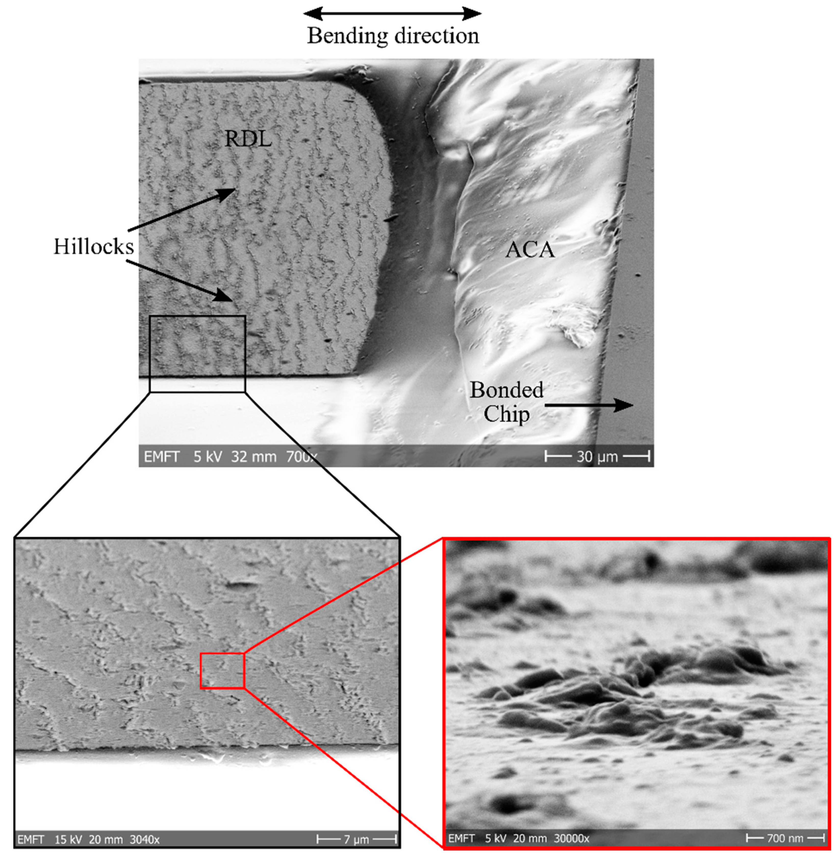
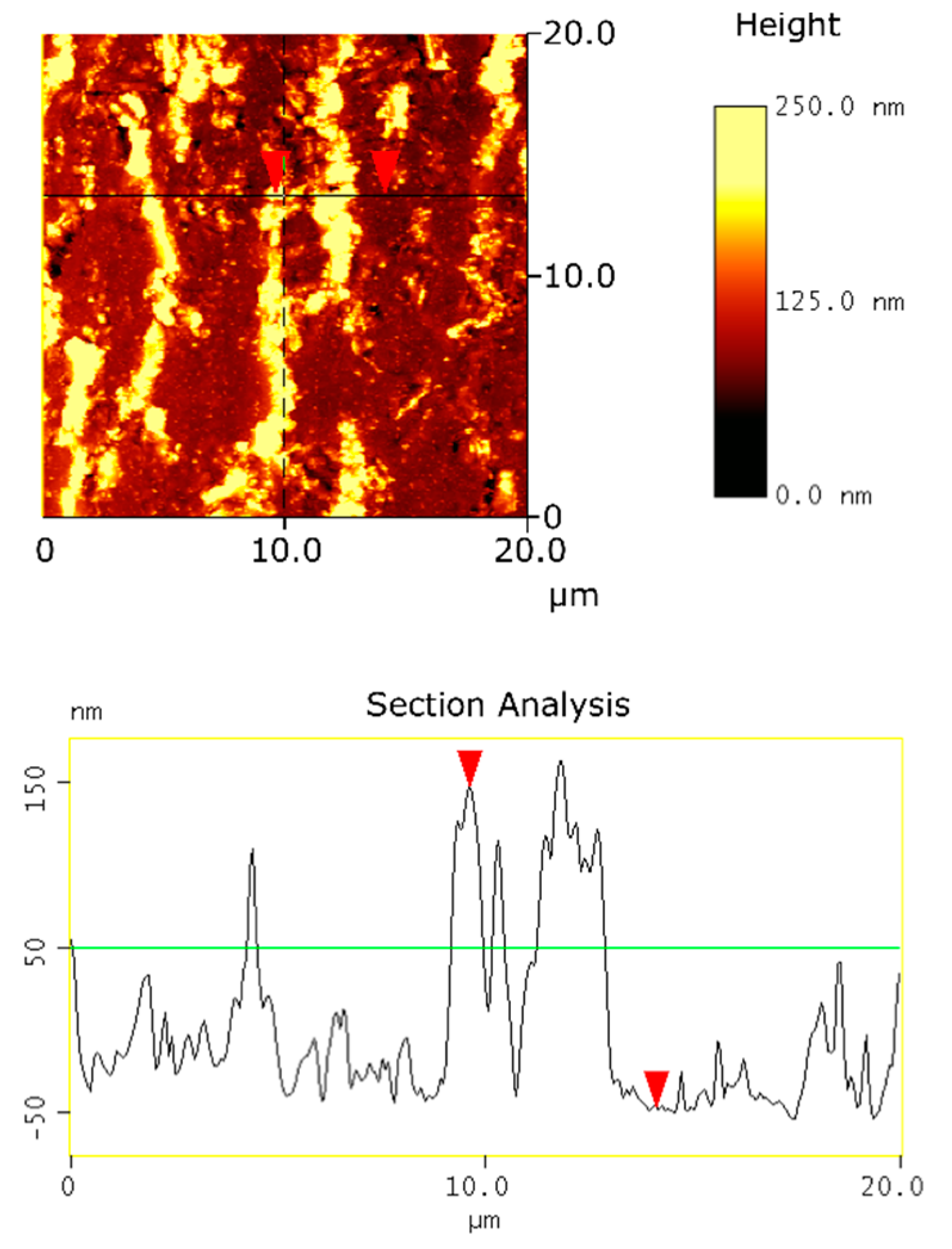
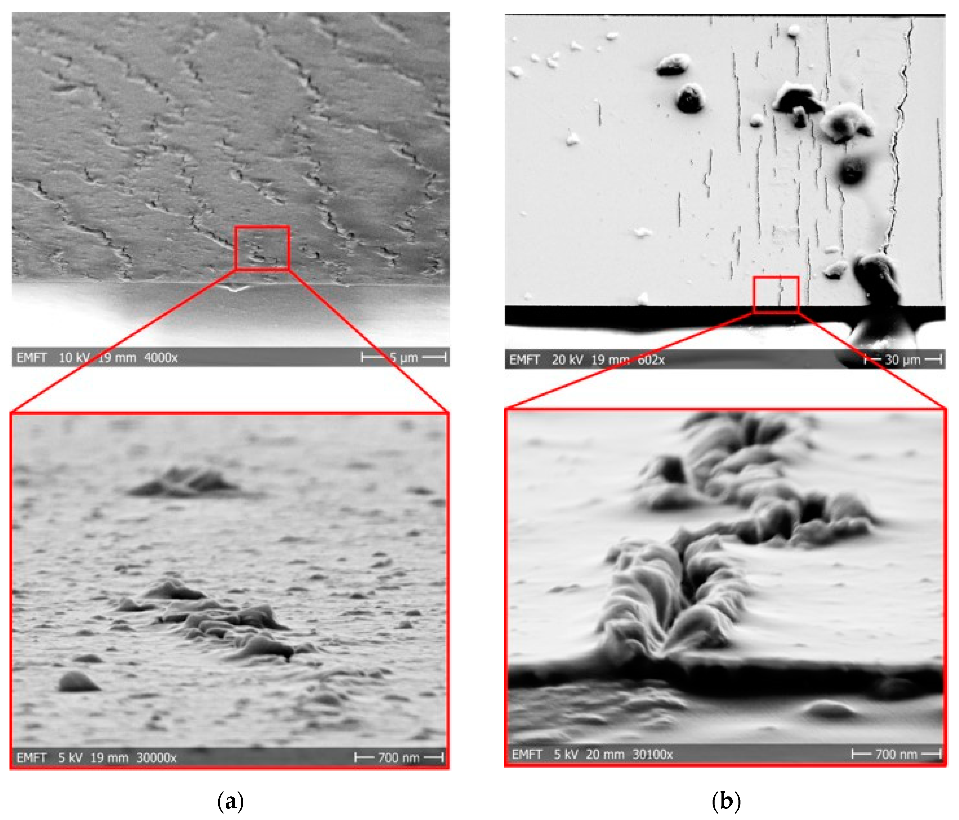
4.1. Optical Analysis

After the completion of 20,000 bending cycles, the chip-foil package test samples were inspected with optical as well as scanning electron microscopy. The analyses revealed that the bonded ultra-thin chips were devoid of any cracks or delamination and the increase in resistance during the tests resulted from the formation of hillocks in the interconnects perpendicular to the direction of bending. Figure 7 shows the hillocks formed on the copper interconnects. Section analysis performed with atomic force microscopy (AFM) revealed that the hillocks had a height of about 250 nm (Figure 8). Similar hillocks were found also on aluminum and gold interconnects (Figure 9 and Figure 10). Several studies indicate that hillocks are created on thin metal layers deposited on foil substrates under repeated bending due to uneven stress distribution arising from thermal and mechanical stresses [50,51,52,53,54,55]. Various mechanisms such as surface roughening and localized differential stress relaxation occurring in the thin metal layer when subjected to repeated mechanical stress have been reported to induce hillocks in thin metal layers [51,52,53,54,55].
The height of hillocks was found to be almost the same (approximately 250 nm) for all three metals (Figure 8 and Figure 10). Therefore, the difference in the increase in daisy chain resistance could plausibly be attributed to the number of hillocks formed in the interconnects since the number of hillocks found on copper interconnects was comparatively higher than the number of hillocks on aluminum and gold interconnects (Figure 7 and Figure 9). Lee et al. have observed that the formation of dislocations and vacancies in thin copper films during bending results in resistance increase [56]. Similar vacancies and dislocations plausibly formed underneath the hillocks could act as electron scattering centers thus increasing the daisy chain resistance. This hypothesis could conceivably be exemplified by correlating the daisy chain resistance increase and the number of hillocks formed in the interconnects. Copper interconnects with the relatively higher number of hillocks exhibited the highest increase in daisy chain resistance whereas gold interconnects with the relatively lower number of hillocks demonstrated the lowest increase in daisy chain resistance. Hence, it could arguably be concluded that the number of hillocks formed on the interconnects is directly proportional to the increase in daisy chain resistance. However, further in-depth investigations are necessary to support this hypothesis. Besides, extensive analysis to determine the exact mechanism behind the formation of hillocks observed in this work is required and this will be comprehensively analyzed in a separate study.

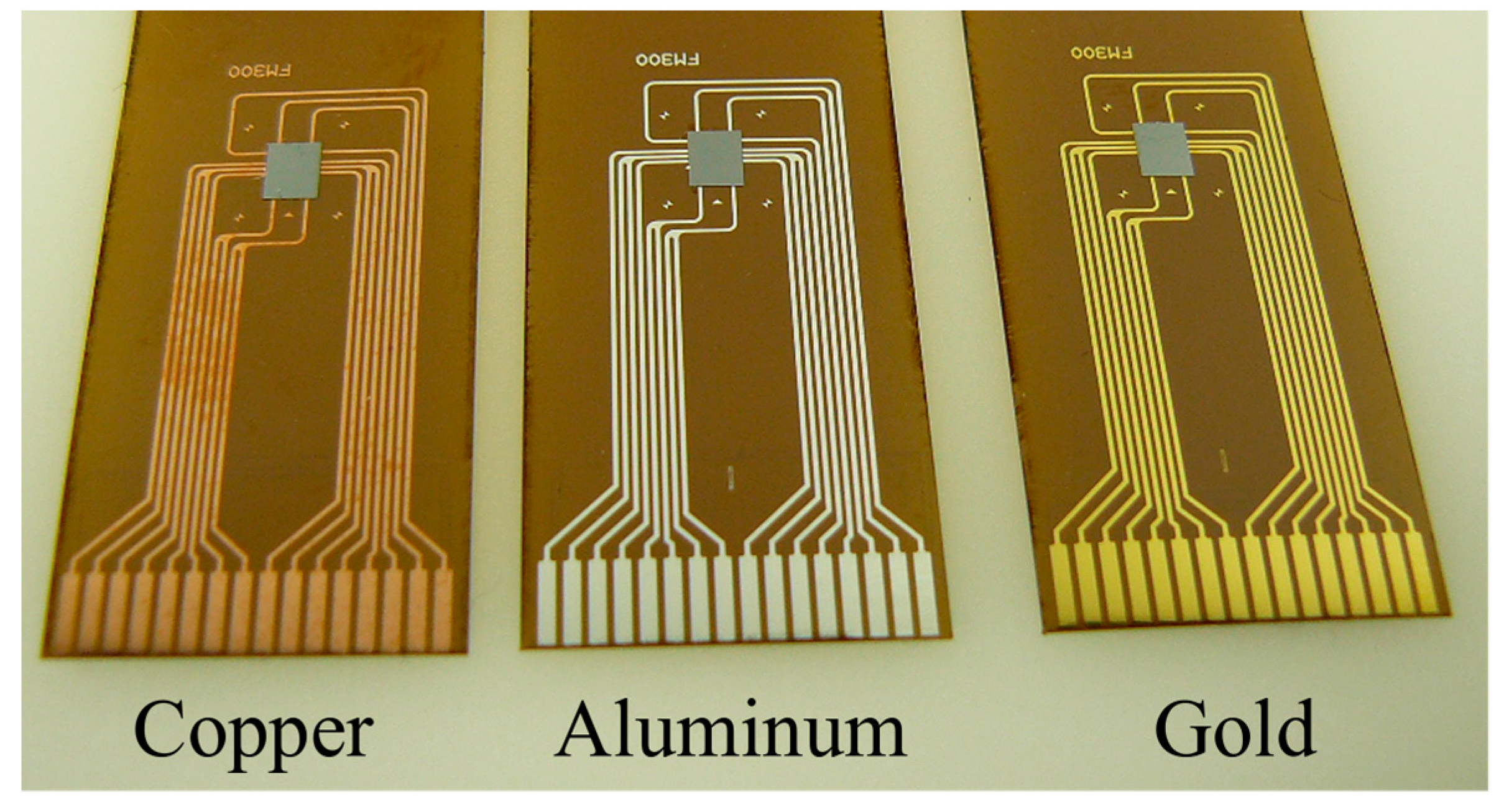
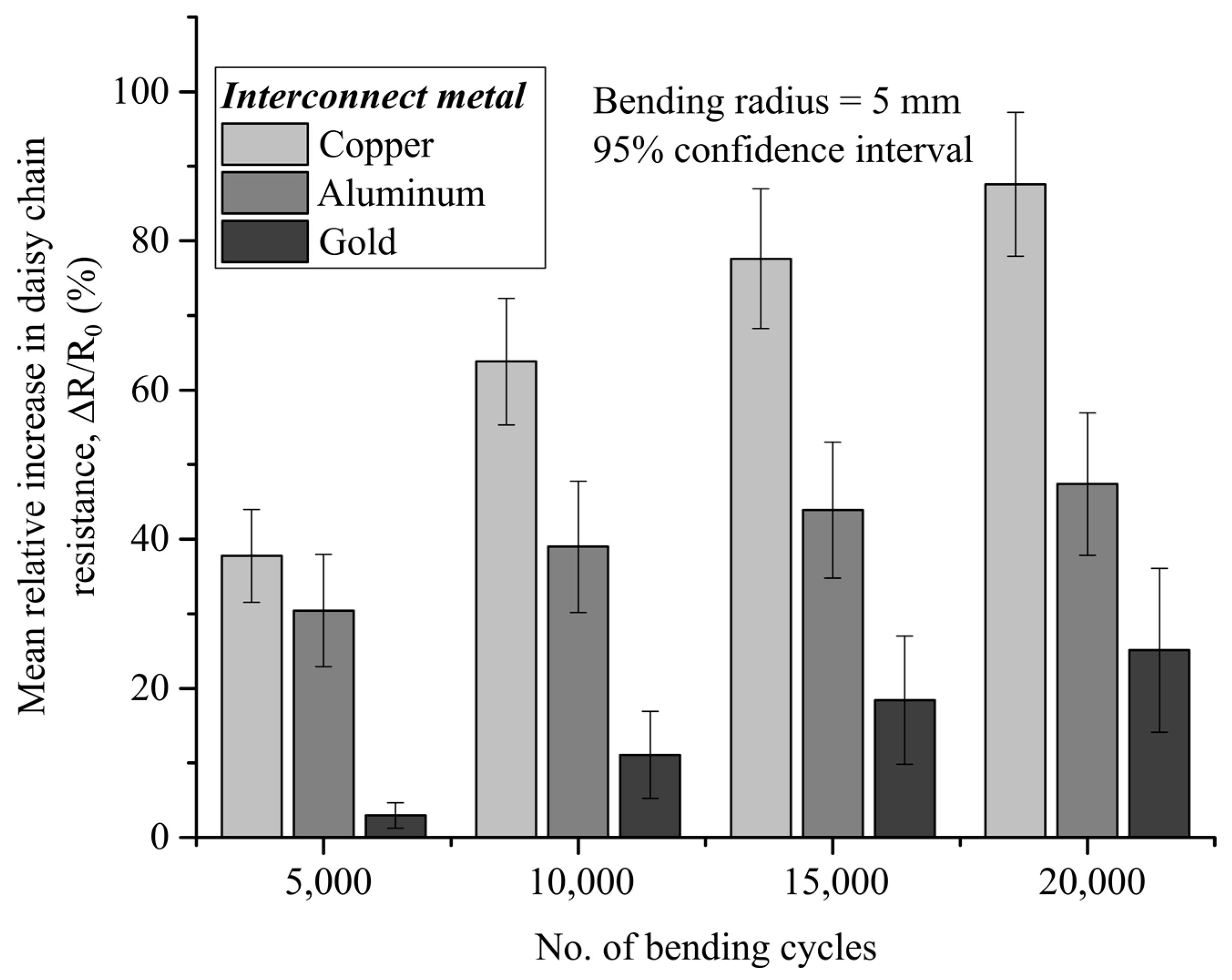
4.2. Choice of Metal for Fabrication of Interconnects

The results of the dynamic bending tests showed that chip-foil packages with gold interconnects are the most flexible followed by aluminum and copper implying that gold could be the favored metal for fabricating interconnects for FHE. However, the higher sheet resistance together with the higher cost of gold compared to copper and aluminum indicate that aluminum could be preferred over gold owing to the decent electrical conductivity as well as good dynamic bending reliability of aluminum.

5. Conclusions

Dynamic bending tests conducted on chip-foil packages revealed a strong influence of flexibility of the metals constituting the interconnects on their dynamic bending reliability. Under repeated bending, the daisy chain resistance of the chip-foil packages increased as the bending cycles progressed. Optical analysis indicated that the increase in daisy chain resistance could plausibly be attributed to the formation and the number of hillocks formed in the interconnects. Test results showed that the chip-foil packages with gold interconnects endured the 20,000 repeated bending cycles at least 3 times better than the chip-foil packages with copper interconnects with a mean increase in resistance of 25.2% compared to 87.6% mean increase for copper interconnects and about 2 times better than the chip-foil package with aluminum interconnects (47.38% mean increase in resistance). However, the higher sheet resistance as well as higher cost of gold indicate that aluminum could instead be favored for fabricating the interconnects due to the decent electrical conductivity and good dynamic bending reliability apart from the relatively lower cost of aluminum.
In the next step, we intend to conduct an in-depth analysis to understand the exact mechanism behind the formation of hillocks. In particular, the influence of the adhesion layer and the foil substrate on the formation of hillocks will be investigated. Afterwards, measures to avoid the formation of hillocks must be devised to improve the dynamic bending reliability of chip-foil packages. Besides, the effect of repeated tensile stress on the dynamic bending reliability of chip-foil packages will also be studied in detail. Furthermore, the reliability of chip-foil packages under torsional bending must be investigated. Finally, environmental tests to examine the corrosion resistance of the chip-foil packages are pivotal for fabricating reliable FHE systems.

Author Contributions

Conceptualization, methodology and investigations, N.P.; sample preparation: W.H., A.D.; manuscript writing, N.P.; manuscript review and editing, C.L., C.K., K.B.; supervision, C.L., C.K., K.B.; funding, C.K. All authors have read and agreed to the published version of the manuscript.

Funding

The research leading to the results presented in this paper were obtained in the scope of the EnSO project that has received funding from (1) the H2020 Framework of the European Union under Grant Agreement no. 692482 and (2) the Bundesministerium für Bildung und Forschung (BMBF) with National Grant no. 16ESE0088.

Acknowledgments

The authors would like to thank Robert Faul, Martin König, Dieter Bollmann, Sabine Scherbaum and Dennise Linke for their support in preparation of the samples that resulted in the fruition of this work.

Conflicts of Interest

The authors declare no conflict of interest.

References

  1. Landesberger, C.; Palavesam, N.; Hell, W.; Drost, A.; Faul, R.; Gieser, H.; Bonfert, D.; Bock, K.; Kutter, C. Novel processing scheme for embedding and interconnection of ultra-thin IC devices in flexible chip foil packages and recurrent bending reliability analysis. In Proceedings of the 2016 International Conference on Electronics Packaging (ICEP), Sapporo, Japan, 20–22 April 2016; IEEE: Sapporo, Japan. [Google Scholar]
  2. Mahsereci, Y.; Saller, S.; Richter, H.; Burghartz, J.N. An ultra-thin flexible CMOS stress sensor demonstrated on an adaptive robotic gripper. IEEE J. Solid State Circuits 2015, 51, 273–280. [Google Scholar]
  3. Bose, I.; Palavesam, N.; Hochreiter, C.; Landesberger, C.; Kutter, C. Low Profile Open MEMS and ASIC Packages Manufactured by Flexible Hybrid Integration in a Roll-to-Roll Compatible Process. In Proceedings of the 2018 48th European Solid-State Device Research Conference (ESSDERC), Dresden, Germany, 3–6 September 2018; IEEE: Dresden, Germany. [Google Scholar]
  4. Gao, W.; Emaminejad, S.; Nyein, H.Y.Y.; Challa, S.; Chen, K.; Peck, A.; Fahad, H.M.; Ota, H.; Shiraki, H.; Kiriya, D.; et al. Fully integrated wearable sensor arrays for multiplexed in situ perspiration analysis. Nature 2016, 529, 509–514. [Google Scholar] [CrossRef] [PubMed] [Green Version]
  5. Kim, J.; Sempionatto, J.R.; Imani, S.; Hartel, M.C.; Barfidokht, A.; Tang, G.; Campbell, A.S.; Mercier, P.P.; Wang, J. Simultaneous monitoring of sweat and interstitial fluid using a single wearable biosensor platform. Adv. Sci. 2018, 5, 1800880. [Google Scholar] [CrossRef] [PubMed] [Green Version]
  6. Oh, S.Y.; Hong, S.Y.; Jeong, Y.R.; Yun, J.; Park, H.; Jin, S.W.; Lee, G.; Oh, J.H.; Lee, H.; Lee, S.-S.; et al. Skin-attachable, stretchable electrochemical sweat sensor for glucose and pH detection. ACS Appl. Mater. Interfaces 2018, 10, 13729–13740. [Google Scholar] [CrossRef]
  7. Sekine, T.; Sugano, R.; Tashiro, T.; Sato, J.; Takeda, Y.; Matsui, H.; Kumaki, D.; Dos Santos, F.D.; Miyabo, A.; Tokito, S. Fully printed wearable vital sensor for human pulse rate monitoring using ferroelectric polymer. Sci. Rep. 2018, 8, 4442. [Google Scholar] [CrossRef]
  8. Khan, Y.; Garg, M.; Gui, Q.; Schadt, M.; Gaikwad, A.; Han, D.; Yamamoto, N.A.D.; Hart, P.; Welte, R.; Wilson, W.; et al. Flexible hybrid electronics: Direct interfacing of soft and hard electronics for wearable health monitoring. Adv. Funct. Mater. 2016, 26, 8764–8775. [Google Scholar] [CrossRef]
  9. Jeong, G.S.; Baek, D.-H.; Jung, H.C.; Song, J.H.; Moon, J.H.; Hong, S.W.; Kim, I.Y.; Lee, S.-H. Solderable and electroplatable flexible electronic circuit on a porous stretchable elastomer. Nat. Commun. 2012, 3, 977. [Google Scholar] [CrossRef]
  10. Strohmeier, P.; Burstyn, J.; Carrascal, J.B.P.; Levesque, V.; Vertegaal, R. ReFlex: A Flexible Smartphone with Active Haptic Feedback for Bend Input. In Proceedings of the TEI’16: Tenth International Conference on Tangible, Embedded, and Embodied Interaction, Eindhoven, The Netherlands, 14–17 February 2016; ACM: Eindhoven, The Netherlands. [Google Scholar]
  11. Loughran, J. Foldable screens and 5G compatibility steal the show at MWC. Eng. Technol. 2019, 14, 9. [Google Scholar] [CrossRef]
  12. Chortos, A.; Liu, J.; Bao, Z. Pursuing prosthetic electronic skin. Nat. Mater. 2016, 15, 937–950. [Google Scholar] [CrossRef]
  13. Gerratt, A.P.; Michaud, H.O.; Lacour, S.P. Elastomeric electronic skin for prosthetic tactile sensation. Adv. Funct. Mater. 2015, 25, 2287–2295. [Google Scholar] [CrossRef]
  14. Wang, C.; Hwang, D.; Yu, Z.; Takei, K.; Park, J.; Chen, T.; Ma, B.; Javey, A. User-interactive electronic skin for instantaneous pressure visualization. Nat. Mater. 2013, 12, 899–904. [Google Scholar] [CrossRef] [PubMed]
  15. Hammock, M.L.; Chortos, A.; Tee, B.C.-K.; Tok, J.B.-H.; Bao, Z. 25th anniversary article: The evolution of electronic skin (e-skin): A brief history, design considerations, and recent progress. Adv. Mater. 2013, 25, 5997–6038. [Google Scholar] [CrossRef] [PubMed]
  16. Yacoub-George, E.; Palavesam, N.; Hell, W.; Koenig, M.; Faul, R.; Landesberger, C. Ultra-thin flexible interposer-a flexible hybrid integration approach to replace wire bonds. In Proceedings of the Smart Systems Integration; 13th International Conference and Exhibition on Integration Issues of Miniaturized Systems, Barcelona, Spain, 10–11 April 2019; VDE: Barcelona, Spain. [Google Scholar]
  17. Christiaens, W.; Bosman, E.; Vanfleteren, J. UTCP: A novel polyimide-based ultra-thin chip packaging technology. IEEE Trans. Components Packag. Technol. 2010, 33, 754–760. [Google Scholar] [CrossRef]
  18. Braun, T.; Becker, K.-F.; Raatz, S.; Minkus, M.; Bader, V.; Bauer, J.; Aschenbrenner, R.; Kahle, R.; Georgi, L.; Voges, S.; et al. Foldable fan-out wafer level packaging. In Proceedings of the 2016 IEEE 66th Electronic Components and Technology Conference (ECTC), Las Vegas, NV, USA, 31 May–3 June 2016; IEEE: Las Vegas, NV, USA. [Google Scholar]
  19. Fang, H.; Yu, K.J.; Gloschat, C.; Yang, Z.; Song, E.; Chiang, C.-H.; Zhao, J.; Won, S.M.; Xu, S.; Trumpis, M.; et al. Capacitively coupled arrays of multiplexed flexible silicon transistors for long-term cardiac electrophysiology. Nat. Biomed. Eng. 2017, 1, 0038. [Google Scholar] [CrossRef] [Green Version]
  20. Burghartz, J.N.; Alavi, G.; Albrecht, B.; Deuble, T.; Elsobky, M.; Ferwana, S.; Harendt, C.; Mahsereci, Y.; Richter, H.; Yu, Z. Hybrid Systems-in-Foil—Combining the Merits of Thin Chips and of Large-Area Electronics. IEEE J. Electron Devices Soc. 2019, 7, 776–783. [Google Scholar] [CrossRef]
  21. Kobayashi, T.; Takeshita, T.; Takei, Y.; Takei, R. Flexible substrate with movable device island supported by serpentine interconnect for mounting ultra-thin silicon chips. In Proceedings of the 2018 International Conference on Electronics Packaging and iMAPS All Asia Conference (ICEP-IAAC), Mie, Japan, 17–21 April 2018; IEEE: Mie, Japan, 2018. [Google Scholar]
  22. Kim, H.; Yoo, H.G.; Hong, S.M.; Jang, B.; Park, D.Y.; Joe, D.J.; Kim, J.-H.; Lee, K.J. Simultaneous roll transfer and interconnection of flexible silicon NAND flash memory. Adv. Mater. 2016, 28, 8371–8378. [Google Scholar] [CrossRef]
  23. Takei, Y.; Nomura, K.-I.; Horii, Y.; Zymelka, D.; Ushijima, H.; Kobayashi, T. Fabrication of Simultaneously Implementing “Wired Face-Up and Face-Down Ultrathin Piezoresistive Si Chips” on a Film Substrate by Screen-Offset Printing. Micromachines 2019, 10, 563. [Google Scholar] [CrossRef] [Green Version]
  24. Gao, H.; Bhat, G.; Ogras, U.Y.; Ozev, S. Optimized Stress Testing for Flexible Hybrid Electronics Designs. In Proceedings of the 2019 IEEE 37th VLSI Test Symposium (VTS), Monterey, CA, USA, 23–25 April 2019; IEEE: Monterey, CA, USA, 2019. [Google Scholar]
  25. Kim, Y.-S.; Lu, J.; Shih, B.; Gharibans, A.; Zou, Z.; Matsuno, K.; Aguilera, R.; Han, Y.; Meek, A.; Xiao, J.; et al. Scalable manufacturing of solderable and stretchable physiologic sensing systems. Adv. Mater. 2017, 29, 1701312. [Google Scholar] [CrossRef]
  26. Palavesam, N.; Marín, S.; Hemmetzberger, D.; Landesberger, C.; Bock, K.; Kutter, C. Roll-to-roll processing of film substrates for hybrid integrated flexible electronics. Flex. Print. Electron. 2018, 3, 014002. [Google Scholar] [CrossRef]
  27. Palavesam, N.; Landesberger, C.; Kutter, C.; Bock, K. A novel test method for robustness assessment of very small, functional ultra-thin chips embedded in flexible foils. In Proceedings of the 10th Smart Systems Integration Conference (SSI 2016), Munich, Germany, 9–10 March 2016. [Google Scholar]
  28. Palavesam, N.; Landesberger, C.; Kutter, C.; Bock, K. Finite element analysis of uniaxial bending of ultra-thin silicon dies embedded in flexible foil substrates. In Proceedings of the 2015 11th Conference on Ph. D. Research in Microelectronics and Electronics (PRIME), Glasgow, UK, 29 June–2 July 2015; IEEE: Glasgow, UK, 2015. [Google Scholar]
  29. Palavesam, N.; Landesberger, C.; Bock, K. Investigations of the fracture strength of thin silicon dies embedded in flexible foil substrates. In Proceedings of the 2014 IEEE 20th International Symposium for Design and Technology in Electronic Packaging (SIITME), Bucharest, Romania, 23–26 October 2014; IEEE: Bucharest, Romania, 2014. [Google Scholar]
  30. Palavesam, N.; Hell, W.; Drost, A.; Landesberger, C.; Kutter, C.; Bock, K. A novel low cost roll-to-roll manufacturing compatible ultra-thin chip integration and direct metal interconnection process for flexible hybrid electronics. In Proceedings of the Additional Conferences (Device Packaging, HiTEC, HiTEN, & CICMT), Copenhagen, Denmark, 11–13 June 2019; No. NOR. International Microelectronics Assembly and Packaging Society: Copenhagen, Denmark; Vol. 2019. [Google Scholar]
  31. Ende, D.V.D.; Van De Wiel, H.; Kusters, R.; Sridhar, A.; Schram, J.; Cauwe, M.; Brand, J.V.D. Mechanical and electrical properties of ultra-thin chips and flexible electronics assemblies during bending. Microelectron. Reliab. 2014, 54, 2860–2870. [Google Scholar] [CrossRef]
  32. Wacker, N.; Richter, H.; Hoang, T.; Gazdzicki, P.; Schulze, M.; A Angelopoulos, E.; Hassan, M.-U.; Burghartz, J.N. Stress analysis of ultra-thin silicon chip-on-foil electronic assembly under bending. Semicond. Sci. Technol. 2014, 29, 095007. [Google Scholar] [CrossRef]
  33. Kim, J.-H.; Lee, T.-I.; Shin, J.-W.; Kim, T.-S.; Paik, K.-W. Bending properties of anisotropic conductive films assembled chip-in-flex packages for wearable electronics applications. IEEE Trans. Components, Packag. Manuf. Technol. 2016, 6, 208–215. [Google Scholar] [CrossRef]
  34. Leber, D.E.; Meek, B.N.; Leija, S.D.; Wilson, D.G.; Chaney, R.L.; Hackler, D.R. Electromechanical reliability testing of flexible hybrid electronics incorporating FleX silicon-on-polymer ICs. In Proceedings of the 2016 IEEE Workshop on Microelectronics and Electron Devices (WMED), Boise, ID, USA, 15 April 2016; IEEE: Boise, ID, USA, 2016. [Google Scholar]
  35. Palavesam, N.; Bonfert, D.; Hell, W.; Landesberger, C.; Gieser, H.; Kutter, C.; Bock, K. Mechanical Reliability Analysis of Ultra-thin Chip-on-Foil Assemblies under different types of recurrent bending. In Proceedings of the 2016 IEEE 66th Electronic Components and Technology Conference (ECTC), Las Vegas, NV, USA, 31 May–3 June 2016; IEEE: Las Vegas, NV, USA, 2016. [Google Scholar]
  36. Palavesam, N.; Yacoub-George, E.; Hell, W.; Landesberger, C.; Kutter, C.; Bock, K. Dynamic Bending Reliability Analysis of Flexible Hybrid Integrated Chip-Foil Packages. In Proceedings of the 2018 IEEE 20th Electronics Packaging Technology Conference (EPTC), Singapore, 4–7 December 2018; IEEE: Singapore, 2018. [Google Scholar]
  37. Liss, K.D.; Qu, D.; Yan, K.; Reid, M. Variability of Poisson’s ratio and enhanced ductility in amorphous metal. Adv. Eng. Mater. 2013, 15, 347–351. [Google Scholar] [CrossRef]
  38. Greaves, G.N.; Greer, A.L.; Lakes, R.S.; Rouxel, T. Poisson’s ratio and modern materials. Nat. Mater. 2011, 10, 823–837. [Google Scholar] [CrossRef] [PubMed]
  39. Gu, X.; Poon, S.J.; Shiflet, G.J.; Widom, M. Ductility improvement of amorphous steels: Roles of shear modulus and electronic structure. Acta Mater. 2008, 56, 88–94. [Google Scholar] [CrossRef]
  40. Oehlers, D.; Seracino, R. Design of FRP and Steel Plated RC Structures: Retrofitting Beams and Slabs for Strength, Stiffness and Ductility; Elsevier: Amsterdam, The Netherlands, 2004; pp. 46–99. [Google Scholar]
  41. Yang, S.-Y.; Yuan, L.-L. Advanced Polyimide Films. In Advanced Polyimide Materials; Elsevier: Amsterdam, The Netherlands, 2018; pp. 1–66. [Google Scholar]
  42. Znajdek, K.; Sibinski, M.; Strąkowska, A.; Lisik, Z. Polymer substrates for flexible photovoltaic cells application in personal electronic system. Opto Electron. Rev. 2016, 24, 20–24. [Google Scholar] [CrossRef]
  43. Sroog, C.E. Films, Mouldings and other Applications. In Polyimides; Springer: Dordrecht, The Netherlands, 1990; pp. 252–284. [Google Scholar]
  44. Landesberger, C.; Scherbaum, S.; Karlheinz, B. Ultra-thin wafer fabrication through dicing-by-thinning. In Ultra-Thin Chip Technology and Applications; Springer: New York, NY, USA, 2011; pp. 33–43. [Google Scholar]
  45. Landesberger, C.; Paschke, C.; Bock, K. Influence of wafer grinding and etching techniques on the fracture strength of thin silicon substrates. In Advanced Materials Research; Trans Tech Publications: Stafa-Zurich, Switzerland, 2011; Volume 325. [Google Scholar]
  46. Delo® Monopox AC245 Technical Information. Available online: https://www.delo-adhesives.com/fileadmin/datasheet/DELO%20MONOPOX_AC245_%28TIDB-GB%29.pdf (accessed on 11 January 2020).
  47. Gouldstone, A.; Koh, H.-J.; Zeng, K.-Y.; Giannakopoulos, A.; Suresh, S. Discrete and continuous deformation during nanoindentation of thin films. Acta Mater. 2000, 48, 2277–2295. [Google Scholar] [CrossRef]
  48. Baek, C.W.; Kim, J.M.; Kim, Y.K.; Kim, J.H.; Lee, H.J.; Han, S.W. Mechanical characterization of gold thin films based on strip bending and nanoindentation test for MEMS/NEMS applications. Sens. Mater. 2005, 17, 277–288. [Google Scholar]
  49. Baek, C.-W.; Kim, Y.-K.; Ahn, Y.; Kim, Y.-H. Measurement of the mechanical properties of electroplated gold thin films using micromachined beam structures. Sens. Actuators A Phys. 2005, 117, 17–27. [Google Scholar] [CrossRef]
  50. Frolov, T.; Boettinger, W.; Mishin, Y. Atomistic simulation of hillock growth. Acta Mater. 2010, 58, 5471–5480. [Google Scholar] [CrossRef]
  51. Wang, D. Fatigue Behavior of Thin Cu Films: Film Thickness and Interface Effects. Ph.D. Thesis, University of Stuttgart, Stuttgart, Germany, 2007. [Google Scholar]
  52. Mönig, R. Thermal Fatigue of Cu Thin Films. Ph.D. Thesis, University of Stuttgart, Stuttgart, Germany, 2005. [Google Scholar]
  53. Eberl, C. Fatigue of Al Thin Films at Ultra High Frequencies. Ph.D. Thesis, University of Stuttgart, Stuttgart, Germany, 2005. [Google Scholar]
  54. Kim, D.-K.; Nix, W.D.; Deal, M.D.; Plummer, J.D. Creep-controlled diffusional hillock formation in blanket aluminum thin films as a mechanism of stress relaxation. J. Mater. Res. 2000, 15, 1709–1718. [Google Scholar] [CrossRef]
  55. Eve, S.; Huber, N.; Last, A.; Kraft, O. Fatigue behavior of thin Au and Al films on polycarbonate and polymethylmethacrylate for micro-optical components. Thin Solid Films 2009, 517, 2702–2707. [Google Scholar] [CrossRef]
  56. Lee, H.-Y.; Yi, S.-M.; Lee, J.-H.; Lee, H.-S.; Hyun, S.; Joo, Y.-C. Effects of bending fatigue on the electrical resistance in metallic films on flexible substrates. Met. Mater. Int. 2010, 16, 947–951. [Google Scholar] [CrossRef]
Figure 1. Scanning electron microscopy image of a typical example of the cross-section of a single contact pad interconnection of a flip-chip bonded chip-foil package.
Electronics 09 00238 g001
Figure 2. Chip-foil package test samples with copper, aluminum and gold interconnects.
Electronics 09 00238 g002
Figure 3. Custom-built test equipment used for performing the dynamic bending tests.
Electronics 09 00238 g003
Figure 4. A chip-foil package test sample connected to the PCB via the zero-insertion force (ZIF) connector.
Electronics 09 00238 g004
Figure 5. (a) Schematic of the test procedure and (b) a bent chip-foil package test sample during a test.
Electronics 09 00238 g005
Figure 6. Mean relative change in daisy chain resistance of chip-foil packages with copper, aluminum and gold interconnects. Relative change in daisy chain resistance, Δ R R 0 =   ( R R 0 ) R 0 × 100 % where R is the daisy chain resistance at the corresponding bending cycle and R0 is the initial daisy chain resistance at the start of the bending tests.
Electronics 09 00238 g006
Figure 7. SEM image showing the hillocks created on the copper interconnect after 20,000 bending cycles.
Electronics 09 00238 g007
Figure 8. Atomic force microscopy (AFM) section analysis of copper interconnect revealing the height of the hillocks.
Electronics 09 00238 g008
Figure 9. SEM images presenting the hillocks formed on (a) aluminum and (b) gold interconnects after 20,000 bending cycles.
Electronics 09 00238 g009
Figure 10. AFM section analysis of (a) aluminum and (b) gold interconnects after 20,000 bending cycles showing the height of the hillocks.
Electronics 09 00238 g010
Table 1. Material properties of the metals used for fabricating interconnects [47,48,49].
MetalSheet Resistance (mΩ/sq)Young’s Modulus (GPa)Poisson’s Ratio
Copper64–781320.33
Aluminum102–110690.33
Gold189–22624.2–43.90.42

