Abstract
This paper presents the fabrication and implementation of novel resistive sensors that were implemented for strain-sensing applications. Some of the critical factors for the development of resistive sensors are addressed in this paper, such as the cost of fabrication, the steps of the fabrication process which make it time-consuming to complete each prototype, and the inability to achieve optimised electrical and mechanical characteristics. The sensors were fabricated via magnetron sputtering of thin-film chromium and gold layer on the thin-film substrates at defined thicknesses. Sticky copper tapes were attached on the two sides of the sensor patches to form the electrodes. The operating principle of the fabricated sensors was based on the change in their responses with respect to the corresponding changes in their relative resistance as a function of the applied strain. The strain-induced characteristics of the patches were studied with different kinds of experiments, such as consecutive bending and pressure application. The sensors with 400 nm thickness of gold layer obtained a sensitivity of 0.0086 Ω/ppm for the pressure ranging between 0 and 400 kPa. The gauge factor of these sensors was between 4.9–6.6 for temperatures ranging between 25 °C and 55 °C. They were also used for tactile sensing to determine their potential as thin-film sensors for industrial applications, like in robotic and pressure-mapping applications. The results were promising in regards to the sensors’ controllable film thickness, easy operation, purity of the films and mechanically sound nature. These sensors can provide a podium to enhance the usage of resistive sensors on a higher scale to develop thin-film sensors for industrial applications.
1. Introduction
The use of sensors for ubiquitous sensing has been a cornerstone for the electronics industry for the last two decades [1,2]. The nature of the sensor being fabricated varies in terms of the fabrication process, processed materials, operating principle, input power and response to ambience conditions. Among these sensors, strain sensing has been one of the fundamental sectors researchers have focused on due to the influence on their use for healthcare [3,4] and industrial [5,6] applications. With respect to the MEMS-based sensors used for strain-sensing, different kinds of flexible sensing prototypes have been developed [7] to enhance their performance in terms of sensitivity, efficiency, gauge factor and longevity. The materials used for their development include different kinds of polymeric substrates and conductive layers to form the substrates and electrodes of the sensors respectively. For example, certain polymers such as polydimethylsiloxane (PDMS) [8,9], polyethylene terephthalate (PET) [10,11], and polyimide (PI) [12,13], have been used extensively to form the sensors. Among them, PI has proven to be one of the most significant due to its ultra-flexibility, mechanical robustness, high thermal stability and resistance towards chemicals and radiation. This makes PI a very popular choice to develop flexible sensors for strain-induced applications [14]. Similarly, for electrodes, even though different kinds of carbon-based allotropes, such as carbon nanotubes [15,16] and graphene [17,18], have been used to form flexible sensors, certain disadvantages—including the high cost of fabrication and short lifetime creates a requirement for alternative conductive materials to be considered for strain-induced applications. To address this requirement, the current paper focuses on the use of commercial polyimide films, sputtering with a thin-film layer of gold to form the conductive sensing surface of the sensors. The reasons for using gold as the sputtered thin-film layer can be attributed to their high electrical conductivity and corrosion resistant nature [19]. The combination of the gold layer with polyimide substrates has been popularised due to its flexibility and multifunctional characteristics [20,21]. Although certain techniques like photolithography [22,23], laser-cutting [24,25], screen printing [26,27], ink-jet printing [28,29] and 3D printing [30,31] have been employed to form sensors, the sputtering technique is shown to have certain advantages over these technologies for forming prototypes. Indeed, the sputtering technique has become one of the most popular methods for developing sensors [32,33]. The advantages of using this technique include the formation of high-purity films, excellent uniformity of the conductive metals on the substrates, controllable film thickness and proper adhesion of the conductive material on the substrates [34]. Although researchers have been working on the fabrication of strain-gauges using sputtering technique [35,36,37], the proposed sensors have advantages over those sputtered-sensors in certain aspects. For example, the steps of fabrication to form a sensor are crucial to validate its usability for ubiquitous monitoring in particular applications. When a sensor is fabricated with small and precise dimensions, its usability largely depends on its large-scale production due to certain factors. For example, the sensors may need to be replaced frequently due to damage or saturation in responses. Thus, it is necessary that the sensing prototypes should be developed with techniques that require minimal steps to fabricate without compromising their characteristics. The developed sensor also has additional advantages, such as being highly robust due to the polyimide substrate, high conductivity of the electrodes, decreasing the complexity of the sensor structure, and increasing the multifunctional capabilities of the sensors. The multi-functionality of these sensors can be highlighted by using them as wearable prototypes that are capable of sustaining prolonged wear and tear due to the robustness of polyimide and thin-film gold layer. Another advantage of the proposed sensors is related to their working principle, as they are cheap and easy to fabricate, possess a higher range of resistance values, and have higher efficiencies and faster responses compared to the capacitive counterparts. Therefore, in comparison to other sensors, the novelty of these sensors can be highlighted as the combined advantages of the fabrication technique and processed materials. The high electrical conductivity, mechanical flexibility and thermal responsiveness of thin-film gold layer; high robustness and mechanical flexibility of the polyimide substrates; and finally, easy operating principle and high purity of the films for the fabrication technique are some of them. The response of these types of sensors towards pressure, strain and temperature are illustrated for the first time in this paper.
The following manuscript has been divided into four sub-sections. Following this introduction, which has shown the originality and purposes for developing these sensors, a detailed explanation of the fabrication processes of the sensor prototypes along with their working principle is next outlined. Section 3 gives the experimental results and corresponding discussion of the results. Finally, the conclusion is given in the final section of the paper.
2. Sensors Used for Experimentation
The sensors’ patches were fabricated in laboratory conditions in conditions with fixed temperature and humidity. Figure 1 shows the schematic diagram of the steps of fabrication of the sensor patches. Commercial polyimide films (ALFA (AESAR, 41896, GH, Haverhill, MA, USA) having a thickness of 8 microns were taken as substrate and attached on acrylic templates with biocompatible tapes (3M 810D Ruban MagiqueMC, Sydney, Australia) for sputtering purposes. Magnetron sputtering was done using an Emitech k550 device to form the conductive layers on the thin-film substrates. This was performed by placing the sample on the middle of the device to obtain the maximum degree of sputtering on the substrates. The samples were initially placed inside the sputtering device, and then chromium and gold were selected as the targets for the sputtering process. Chromium was used for better adhesion of gold layer on the polyimide substrates. The phenomenon took place in the plasma environment where the current varied between 0 and 20 mA. The thickness of the chromium layer was kept fixed at 20 nm, while the thickness of the gold layer was varied between 200 nm and 400 nm to determine the correct level for optimised performances. This method of selecting the thickness of sputtered gold was based on some of the previous research [38,39] done by our group on MEMS-based sensors. In the previous work, the thickness of the chromium layer was chosen to be 20 microns, while 500 microns was set for the gold layer. In the current work, we set the range of the thickness of the thin-film gold layer between 200 nm and 500 nm with a difference of 100 nm. The quality of these four thicknesses was determined based on the consistency of their responses and the adhesive of the sputtered gold layer. The surface adhesion of gold layers was measured to determine the robustness of the sensors for different thicknesses via a series of experiments of consecutive bending and response to temperature. It was found out that among these four thicknesses, the sensors with a thickness of 400 nm achieved the best results for both response and surface adhesion. For 400 nm thickness of the gold layer, the resistance values for different cycles were much more constant, and the adhesion of the sputtered gold layer was also better after a series of experiments. When the thickness of the gold layer was increased to 500 nm, the sensor response did not vary from that of 400 nm. So, the final values for the thin-film layers for the fabrication of the sensors were decided to 20 nm and 400 nm for gold and chromium respectively. Following the sputtering process, the samples were carefully taken off the template and cut into sizes with a length of 30 mm and a width of 20 mm to form the sensor patches. The two sides of each of the prototype were attached with copper tapes (Hi-Bond HB 720A, RS Components, Corby, UK) to form the electrodes.
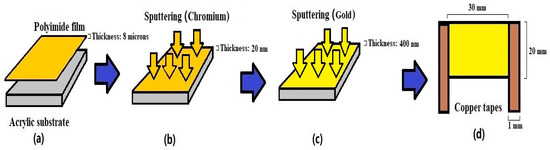
Figure 1.
Schematic diagram of the steps of fabrication for the gold-polyimide sensors. (a) After attaching the polyimide films onto the acrylic dishes with tapes, (b) the thin-films were sputtered with chromium and gold to form the sensing area of the samples. (c,d) The films were then taken off the template and attached to copper tapes on two sides to form the electrodes of the sensor patches.
Figure 2 shows the output result of the sputtering process, which was taken off the sputtering device for experimental processes. Figure 3 shows the Scanning Electron Microscopic (SEM) image of the sputtered sensor. The zoomed view in the image shows the smoothness of the sputtering on a micro level. It can be seen that there are some black spots in the image in contrast to the sputtering white regions. These black spots represent the regions where the sputtering did not happen evenly. This could be due to the shadowing effect, which plays a pivotal role in the distribution of the incident particle flux. The reasons for this effect can be attributed to the angular distribution of the incident atoms on a long-range surface [40] or could be due to the irregular surface diffusion of the sensing area due to the roughening of the surface [41]. Although some of the regions display an uneven sputtering of gold or chromium, most parts of the sensor had a consistent sputtered layer of chromium and gold on the polyimide substrate. The unevenness of the sputtering of the thin-film gold layer in some regions did even affect the electrical and mechanical performance of the sensors. The final sensor patch is shown in Figure 4, where its size is compared to an AUD 20 cent to depict its miniaturised nature. The small size of the sensors increases their potential to be used for wearable sensing purposes.
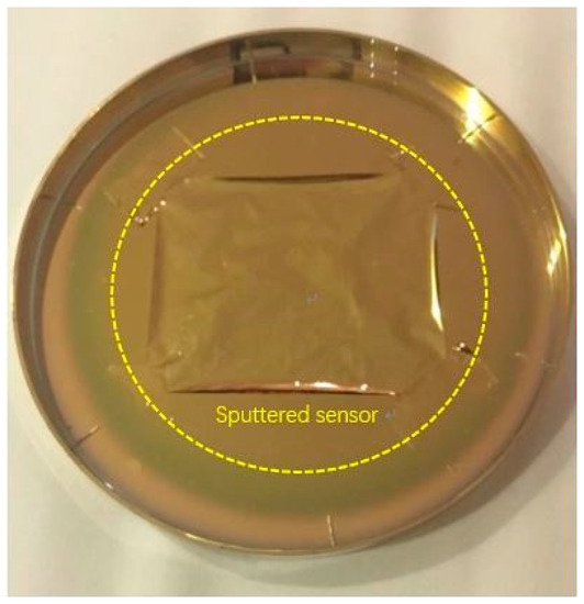
Figure 2.
The polyimide film with a thickness of 8 microns on an acrylic dish sputtered with chromium and gold.
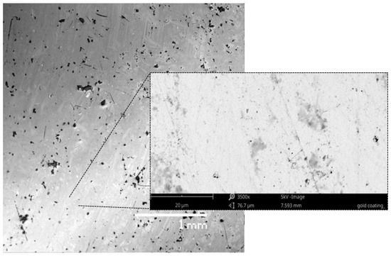
Figure 3.
SEM image of the sputtered sensor. The zoomed view shows the quality of the sputtering on the sensing surface.
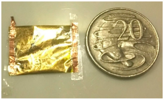
Figure 4.
Comparison of the size of the finished sample with an AUD 20 cents.
Figure 5 shows the schematic diagram of the equivalent circuit of the sensors depicting the conditions before and after the application of pressure [42]. Along with the internal electrode resistive elements, the sensor also consists of a piezoresistive element that exists between the electrodes. When the dimension changes, the orientation of the thin-film layer simultaneously changes, resulting in variation in the resultant resistance [43]. When pressure is applied to the sensing area, the sensors undergo a tensile strain, increasing the change in relative resistance [44]. Since the sensing area of the prototypes consists of a gold and chromium sputtered thin-film layer, this increase is dictated by their conducting paths. When the pressure is released, the shape of the sensors returns to its original position, thus obtaining its initial response. However, in the case of consecutive bending experiments, the sensors operated in a compressive mode, which is opposite to that of the tensile mode operation. In this case, the bending of the sensors increased the conducting paths on the sputtered layer, thus decreasing the relative resistance. The sensors have been tested for consecutive bending, tactile sensing and changes in responses with respect to pressure and temperature. Fifty samples had been used for each of the experiments to validate the repeatability in the responses of these fabricated sensors.
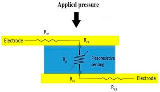
Figure 5.
The working principle of the resistive sensors. The sensor consists of a variable resistor, which is the piezoresistive sensing element [42]. The resistive values of this element vary according to the magnitude and direction of the pressure applied to the sensors.
3. Results and Discussion
The sensors were employed for different kinds of strain-sensing applications where they were subjected to variable inputs in terms of pressure and temperature to determine their corresponding outputs. The change in the output of the sensors with respect to the applied pressure on the sensing surface was determined in terms of the change in relative resistance, as shown in the equivalent circuit in Figure 5. The responses were monitored using a HIOKI IM 3536 LCR metre that was connected to the copper tapes of the sensors via Kelvin probes. The impedance analyser, in turn, was connected to a laptop via a USB cable to collect the monitored data in Microsoft Excel using an automated data acquisition algorithm. Due to the resistive nature of the sensors, the instrument was operated in a DC mode where the voltage was varied to determine the changes in relative resistance and current. Firstly, the sensors were subjected to consecutive bending to determine the repeatability of their results. Figure 6 shows the output of the consecutive bending test where the sensors were bent in an oscillatory motion to determine the changes in the corresponding resistances. The bending was done manually to change the dimension of the sensors. The direction of the bending of the sensors is shown in the inset of Figure 6. The sensors were bent to a limit with a bending radius curvature of 12 mm. This value was chosen to avoid any kind of contact between the electrode tapes while in the bent position. The direction of the strain was perpendicular to the electrodes. The number of oscillatory cycles was continued to around 100 cycles to validate the repeatability of the response of the sensors. The number of cycles was limited to 100 as after this; the sensors started to acquire a bent shape in the direction of the bending. It is seen from Figure 6 that the sensors generated a constant response over the entire duration. Three cycles were randomly chosen (450–700 s) from this duration to distinguish the two positional differences of the sensors. Two different situations, namely ‘normal’ and ‘bent’ positions, have been considered for the conditions referring to the extended and flexed positions respectively for the sensors. The normal and bent positions in Figure 6 were ascribed as ‘N’ and ‘B’ respectively.
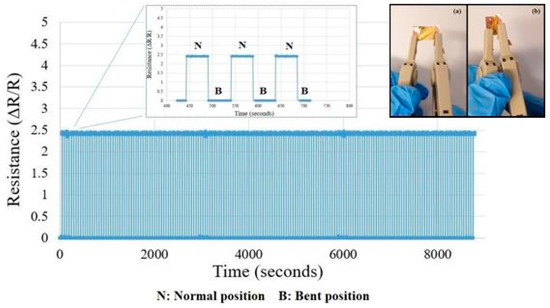
Figure 6.
Consecutive bending of the gold-polyimide sensors to determine the repeatability in the changes in their responses. The inset of the figure shows the (a) normal and (b) bent positions.
The resistance of the sensors decreased as the position was changed from normal to bent. The decrease in the relative resistance with respect to the applied strain can be attributed to the increase in current in the sensors, which is due to the increase in the interlinked connections of the gold particles in the sensing area of the prototypes. The sensors exerted very similar responses with each cycle, thus validating their repeatability. The response time of the sensors was less than one second. The repeatable nature in the response of these sensors is important for monitoring human motions, like flexible strain gauges [45,46]. The second experiment conducted on the sensor patches was to determine the change in relative resistance with respect to a change in pressure. The pressure was applied using a pressure tester metre SF500N. The pressure was applied centred on the sensing area of the prototypes. The change in the response with respect to pressure was studied for the three types of sensors, as shown in Figure 7. The range of pressure was kept constant between 0–400 kPa as this is the limit of pressure exerted on sensors in tactile sensing with human tactile sensing applications [47,48]. As can be seen from Figure 7, the sensors showed small resistive changes for the three types of sensors. The highest change in resistance took place for the sensor having a thickness of 200 nm of the thin-film gold layer. The reason for this phenomenon can be attributed to the increase in the current as a result of the increase in the inter-particle connection between the gold particles with a corresponding increase in the thickness in the layer. The sensitivity of the sensors was determined for the sensors having a thickness of 400 nm for the gold layer. Figure 8 shows the change in response of the sensors, where a linear trend line is fitted to obtain the slope. As seen from the figure, the sensitivity of these sensors for the pressure ranging between 0 and 400 kPa is 0.0086 Ω/ppm. The next experiment was performed by testing the behaviour of the sensors at a range of temperatures. Even though these sensors have been fabricated for strain-sensing purposes, the reason for analysing their behaviour with respect to temperature was to determine the temperature coefficient of resistance (α) of these sensors. Figure 9 shows the change in the resistance with respect to the temperature being varied between 25 °C and 85 °C. It is seen that the resistance values vary almost linearly with the temperature with a high coefficient of determination (R2). From Figure 8, the coefficient of thermal expansion was calculated to be around 0.016 Ω/°C. In accordance with the above two experiments, the sensors also responded to the changes in pressure for four different temperature values of 25 °C, 35 °C, 45 °C and 55 °C.
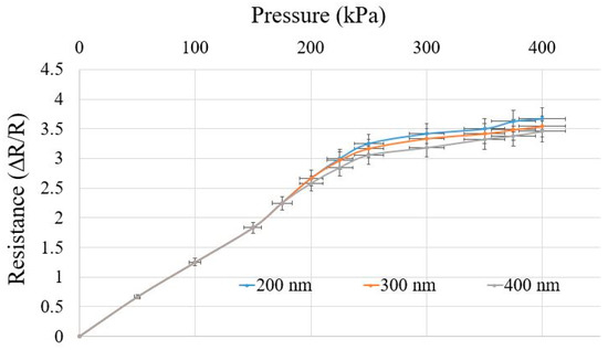
Figure 7.
The response of the sensors for the change in pressure ranging between 0 and 400 kPa. The experiments were done on three types of prototypes differing in the thickness of the gold layer for 200 nm, 300 nm and 400 nm.
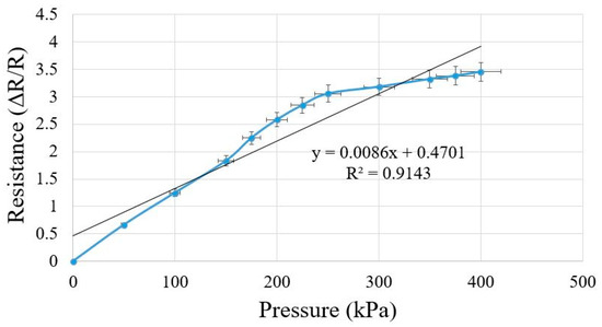
Figure 8.
The variation of relative resistance with respect to pressure for sensors with 400 nm. The sensitivity of the sensors for this range was 0.0086 Ω/kPa.
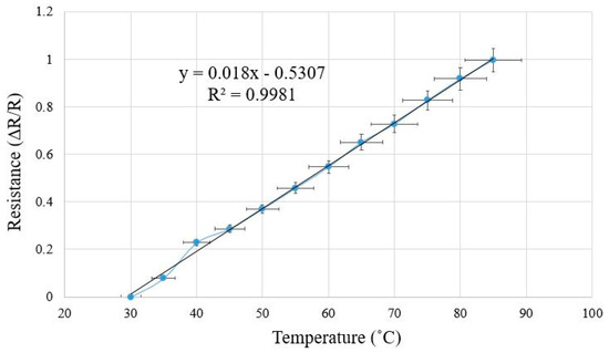
Figure 9.
The response of the sensors for the change in temperature ranging between 30 °C and 85 °C.
The reason for choosing these four temperature values can be attributed to most of the human-related tactile sensing experiments taking place within this range [49]. Figure 10 shows the change in the relative resistance with respect to the increase in pressure for the four values of temperature. The change in relative resistance increases with temperature for a particular pressure is due to the properties of the gold thin-films [50,51,52]. The reason behind this phenomenon can be attributed to the vibrational effect of the sputtered layer about their home positions, which causes an increase in thermal energy. The gauge factor (GF) was calculated for these temperature values to determine the variation with respect to temperature. It was seen that the G.F. varied between 4.9–6.6 when the temperature was increased from 25 °C to 55 °C.
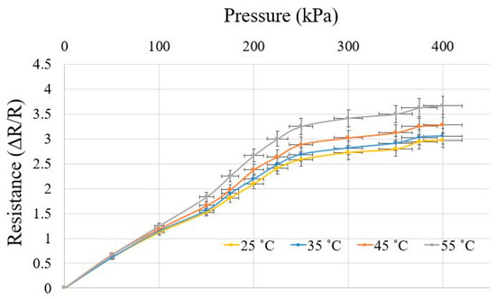
Figure 10.
The response of the sensors with respect to the change in pressure for four different temperatures of 25 °C, 35 °C and 45 °C and 55 °C.
Along with the advantages of these sensors described above in terms of their fabrication and processed materials, these sensors exhibited a reasonably high G.F. The G.F. value was higher than other strain sensors that were polyimide-based [53,54], silicon-based [55] and fabric-based [56] used for biomedical applications. Figure 11 shows the change in the relative resistance of the sensors with respect to the induced strain in the vertical direction. The tensile strain was applied to the sensors using an EXCEED E42 Universal Testing Machine from MTS by clamping the two sides of the sensors. One of the sides was kept fixed, while the other was moved vertically upwards under its breaking point. The change in response was recorded simultaneously with the applied tensile strain. It was seen that the vibration in relative resistance was almost linear with a high R2 value for the range of strain considered for the sensor patches.
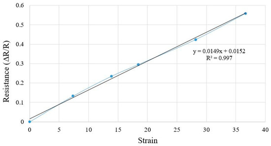
Figure 11.
The response of the sensors in terms of change in relative resistance for the applied strain.
Next, the sensors were tested for tactile measurements where manual pressure was applied on the sensing (sputtered) area of the sensor patches. The sensor patches were fixed in one location with sticky tapes, and then their sensing area was touched. The reason for opting for manual pressure is to show the potentiality of these sensors for soft-touch tactile measurements [57]. Figure 12 shows the response of the patches to tactile sensing, while the inset of the figure shows the setup of applying pressure on the sensors. Two terms, namely ‘touched’ and ‘untouched’, denoted by ‘T’ and ‘U’, refers to the conditions of touching and refraining from touching the finger to the sensing area of the patches respectively. The tactile experiments were performed successfully with the relative resistance varying between two fixed ranges for the two corresponding conditions. It is seen that the range of resistance for tactile sensing is a little higher than in the other pressure sensing experiments. This behaviour can be attributed to two reasons: firstly, the change in the response was additionally affected by the permittivity of the skin; secondly, due to the exertion of a manual force on the skin, the pressure applied on the sensors for tactile sensing can be more than that of the other experiments. One of the reasons why the sensors did not obtain the same values when the pressure was released is possibly because the sputtered thin-film layers did not obtain the same orientation as they had in the previous cycle. When the sensor went back to the untouched position, due to the ultra-thin thickness of the substrates, the sensing area did not necessarily re-occupy its original shape, thus causing a slight change in the output resistance. The response of the sensors based on gentle touching can be considered when employing these sensors for tactile applications in electronic skins [58,59].
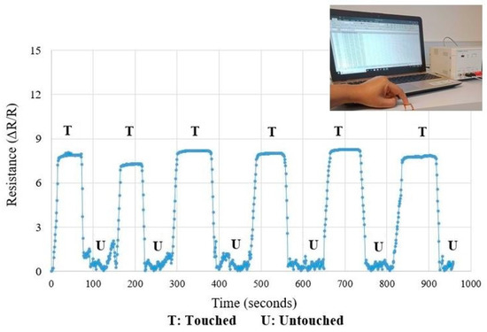
Figure 12.
Tactile sensing experiments performed on the developed patches. The inset of the figure shows the positioning of the index finger on the sensing area of the patches.
The next experiment for strain-induced applications was the change in the degree of the tensile strain applied on the sensor patches. This experiment tested the differences in the pressures exerted on the sensor patches for soft-touch tactile and robotic arm applications. Tensile stress measuring equipment (EXCEED E42 Universal Test Systems from MTS) was used for the experiments, and the prototypes were clamped from two sides. Due to the ultra-thin nature of the sensors, the connections were made carefully to avoid any bending during the clamping process, which could have affected the response of the sensors. One of the sides were pulled, keeping the side constant to determine the changes in relative resistance and current. The degree of strain was conducted by varying its amount for the sensors being in little stretched to full stretched condition. The little stretching of the sensors refers to the point where the sensors move a little bit from their initial position, where the fully stretched position refers to the situation just before breaking off the sensor. However, there was one assumption made during the simultaneous application of stress and the monitoring of the data. During the sputtered nature of the sensing surface, the effect of the cracking of the thin-film layer beyond a certain limit of stretching was considered negligible to avoid the complicacy of interconnection between the surface effects of polyimide and thin-film gold layer. The effect of cracking on the sensing surface demands a new field of study to determine the difference in responses caused due to the tension between the sputtered gold layer and the substrates beneath it. Figure 13 and Figure 14 show the change in the relative resistance and current respectively for different amounts of tensile strain. The relative change in resistance of the sensor patches increased on the application of the tensile strain, whereas the three consecutive cycles for each degree of stretching displayed a similar range of resistance values. Due to the increase in the relative resistance with respect to the applied strain, the corresponding output current decreased, as shown in Figure 14. The response of the sensor patches for different degrees of tensile strain can be advantageous for their uses in robotic industries, where the degree of strain can sometimes be a function of the amount of movement of robotic arms.
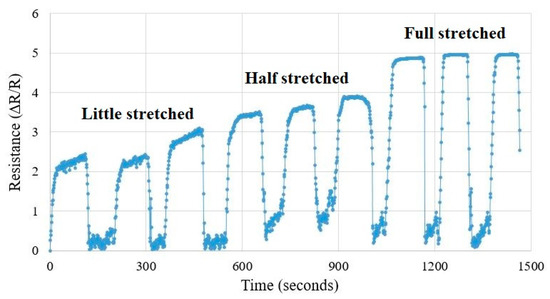
Figure 13.
The response of the sensor patches with respect to the variation of tensile strain applied to them. The stretching of the sensors was varied from little stretched to full stretched condition to determine the increase in the corresponding resistance values.
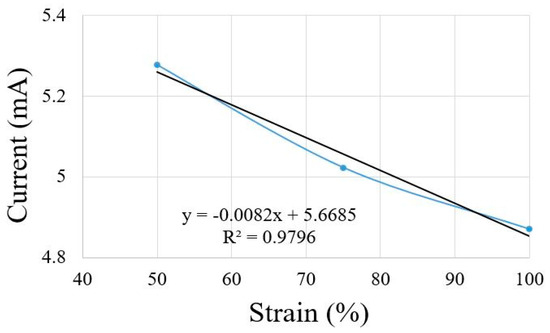
Figure 14.
Change in current with respect to different degrees of tensile strain.
4. Conclusions
The paper showcases the fabrication and implementation of novel sensor patches developed from thin-film gold layer and polyimide films. Sputtering of chromium and gold layers at defined thicknesses was performed using the magnetron sputtering technique. Some of the advantages of these developed sensors lie in their easy operating principle, high robustness, quick response to the strain-sensitive changes, high electrical conductivity, purity of the sputtered films, proper adhesion of the conductive layer on the substrate and overall mechanical flexibility. The sensors were then employed for different strain-sensing applications to determine their responses in terms of the change in the relative resistance. The strain-sensing experiments were performed to determine their capability to perform real-time tactile experiments. The developed patches exhibited excellent outputs in terms of quick response and repeatability with respect to the change in inputs. A sensitivity and GF of 0.0086 Ω/ppm and 4.4–6.9 respectively was obtained for the sensors having sputtered layers of 20 nm of chromium and 400 nm of gold. One of the issues faced during the experimental process was the presence of some glitches in the outputs. There can be two possible reasons for this behaviour: firstly, the Kelvin probes connected to the sensors might be loosened or stretched during the procedure, which can lead to non-identical data for consecutive cycles; secondly, the interlinked connections between the gold particles might not be the same for two cycles to produce dissimilar data. The remedy for this issue can be an association of wireless systems [60] with the sensors where the data can be processed and sent via microcontroller-based embedded systems to the monitoring unit without the involvement of any physical wire-related connections. The second issue faced was the dissimilarity in the results for consecutive cycles under different degrees of tensile strain. This can be attained by introducing dynamic thresholding [61] to the response of the sensors to distinctively classify the outputs for different input conditions. The usability of these sensors can be considered to form enhanced resistive sensors and to subsequently utilise them for monitoring purposes.
Author Contributions
Conception and design, T.H., A.N.; collection and assembly of data, A.N., N.A.; data analysis and interpretation, A.N., N.A., F.A., H.L. and S.S.; manuscript writing, T.H., A.N.; supervision, T.H., S.M. and Y.X.; funding, T.H., Y.X.
Funding
This work was supported in part by International Scientific and Technological Cooperation Project of Dongguan (2016508102011), in part by Guangdong Provincial Key Platform and Major Scientific Research Projects (2017GXJK174) and in part by Science and Technology Innovation Special Fund Project of Guangdong Province (2018A050506086).
Acknowledgments
The authors would like to thank the microscopy department of Macquarie University, Australia for providing the SEM images of the sensors. The authors are also thankful to Robyn Bray, director of the DCI Language Centre in Dongguan University of Technology, Dongguan, for her assistance in improving the quality of the manuscript in terms of its language.
Conflicts of Interest
The authors declare no conflict of interest.
References
- Wang, J. Electrochemical glucose biosensors. Chem. Rev. 2008, 108, 814–825. [Google Scholar] [CrossRef] [PubMed]
- Ge, G.; Huang, W.; Shao, J.; Dong, X. Recent progress of flexible and wearable strain sensors for human-motion monitoring. J. Semicond. 2018, 39, 011012. [Google Scholar] [CrossRef]
- Agarwala, S.; Goh, G.L.; Dinh Le, T.-S.; An, J.; Peh, Z.K.; Yeong, W.Y.; Kim, Y.-J. Wearable Bandage-Based Strain Sensor for Home Healthcare: Combining 3D Aerosol Jet Printing and Laser Sintering. ACS Sens. 2018, 4, 218–226. [Google Scholar] [CrossRef]
- Eswaraiah, V.; Balasubramaniam, K.; Ramaprabhu, S. Functionalized graphene reinforced thermoplastic nanocomposites as strain sensors in structural health monitoring. J. Mater. Chem. 2011, 21, 12626–12628. [Google Scholar] [CrossRef]
- Takao, H.; Sawada, K.; Ishida, M. Monolithic silicon smart tactile image sensor with integrated strain sensor array on pneumatically swollen single-diaphragm structure. IEEE Trans. Electron Devices 2006, 53, 1250–1259. [Google Scholar] [CrossRef]
- Oh, J.; Yang, J.C.; Kim, J.-O.; Park, H.; Kwon, S.Y.; Lee, S.; Sim, J.Y.; Oh, H.W.; Kim, J.; Park, S. Pressure Insensitive Strain Sensor with Facile Solution-Based Process for Tactile Sensing Applications. ACS Nano 2018, 12, 7546–7553. [Google Scholar] [CrossRef]
- Nag, A.; Mukhopadhyay, S.C.; Kosel, J. Wearable Flexible Sensors: A Review. IEEE Sens. J. 2017, 17, 3949–3960. [Google Scholar] [CrossRef]
- Lei, K.F.; Lee, K.-F.; Lee, M.-Y. Development of a flexible PDMS capacitive pressure sensor for plantar pressure measurement. Microelectron. Eng. 2012, 99, 1–5. [Google Scholar] [CrossRef]
- Mannsfeld, S.C.; Tee, B.C.; Stoltenberg, R.M.; Chen, C.V.H.; Barman, S.; Muir, B.V.; Sokolov, A.N.; Reese, C.; Bao, Z. Highly sensitive flexible pressure sensors with microstructured rubber dielectric layers. Nat. Mater. 2010, 9, 859. [Google Scholar] [CrossRef]
- Yaqoob, U.; Phan, D.-T.; Uddin, A.I.; Chung, G.-S. Highly flexible room temperature NO2 sensor based on MWCNTs-WO3 nanoparticles hybrid on a PET substrate. Sens. Actuators B Chem. 2015, 221, 760–768. [Google Scholar] [CrossRef]
- Kwak, Y.H.; Choi, D.S.; Kim, Y.N.; Kim, H.; Yoon, D.H.; Ahn, S.-S.; Yang, J.-W.; Yang, W.S.; Seo, S. Flexible glucose sensor using CVD-grown graphene-based field effect transistor. Biosens. Bioelectron. 2012, 37, 82–87. [Google Scholar] [CrossRef]
- Xiao, S.; Che, L.; Li, X.; Wang, Y. A novel fabrication process of MEMS devices on polyimide flexible substrates. Microelectron. Eng. 2008, 85, 452–457. [Google Scholar] [CrossRef]
- Qin, Y.; Peng, Q.; Ding, Y.; Lin, Z.; Wang, C.; Li, Y.; Xu, F.; Li, J.; Yuan, Y.; He, X. Lightweight, superelastic, and mechanically flexible graphene/polyimide nanocomposite foam for strain sensor application. ACS Nano 2015, 9, 8933–8941. [Google Scholar] [CrossRef] [PubMed]
- Wang, Y.; Wang, A.X.; Wang, Y.; Chyu, M.K.; Wang, Q.-M. Fabrication and characterization of carbon nanotube–polyimide composite based high temperature flexible thin film piezoresistive strain sensor. Sens. Actuators A Phys. 2013, 199, 265–271. [Google Scholar] [CrossRef]
- Tadakaluru, S.; Thongsuwan, W.; Singjai, P. Stretchable and flexible high-strain sensors made using carbon nanotubes and graphite films on natural rubber. Sensors 2014, 14, 868–876. [Google Scholar] [CrossRef] [PubMed]
- Jeong, H.Y.; Lee, D.-S.; Choi, H.K.; Lee, D.H.; Kim, J.-E.; Lee, J.Y.; Lee, W.J.; Kim, S.O.; Choi, S.-Y. Flexible room-temperature NO2 gas sensors based on carbon nanotubes/reduced graphene hybrid films. Appl. Phys. Lett. 2010, 96, 213105. [Google Scholar] [CrossRef]
- Chung, M.G.; Kim, D.-H.; Seo, D.K.; Kim, T.; Im, H.U.; Lee, H.M.; Yoo, J.-B.; Hong, S.-H.; Kang, T.J.; Kim, Y.H. Flexible hydrogen sensors using graphene with palladium nanoparticle decoration. Sens. Actuators B Chem. 2012, 169, 387–392. [Google Scholar] [CrossRef]
- Wang, Y.; Yang, R.; Shi, Z.; Zhang, L.; Shi, D.; Wang, E.; Zhang, G. Super-elastic graphene ripples for flexible strain sensors. ACS Nano 2011, 5, 3645–3650. [Google Scholar] [CrossRef]
- Ahmed, R.A.; Fadl-allah, S.A.; El-Bagoury, N.; El-Rab, S.M.G. Improvement of corrosion resistance and antibacterial effect of NiTi orthopedic materials by chitosan and gold nanoparticles. Appl. Surf. Sci. 2014, 292, 390–399. [Google Scholar] [CrossRef]
- Kim, T.; Lee, T.; Lee, G.; Choi, Y.W.; Kim, S.M.; Kang, D.; Choi, M. Polyimide Encapsulation of Spider-Inspired Crack-Based Sensors for Durability Improvement. Appl. Sci. 2018, 8, 367. [Google Scholar] [CrossRef]
- Putz, B.; Glushko, O.; Cordill, M.J. Electromigration in gold films on flexible polyimide substrates as a self-healing mechanism. Mater. Res. Lett. 2016, 4, 43–47. [Google Scholar] [CrossRef] [PubMed]
- Acuautla, M.; Bernardini, S.; Gallais, L.; Fiorido, T.; Patout, L.; Bendahan, M. Ozone flexible sensors fabricated by photolithography and laser ablation processes based on ZnO nanoparticles. Sens. Actuators B Chem. 2014, 203, 602–611. [Google Scholar] [CrossRef]
- Pal, R.K.; Farghaly, A.A.; Collinson, M.M.; Kundu, S.C.; Yadavalli, V.K. Photolithographic micropatterning of conducting polymers on flexible silk matrices. Adv. Mater. 2016, 28, 1406–1412. [Google Scholar] [CrossRef] [PubMed]
- Nag, A.; Mukhopadhyay, S.; Kosel, J. Transparent biocompatible sensor patches for touch sensitive prosthetic limbs. In Proceedings of the 10th International Conference on Sensing Technology (ICST), Nanjing, China, 11–13 November 2016; pp. 1–6. [Google Scholar]
- Nag, A.; Mukhopadhyay, S.; Kosel, J. Influence of temperature and humidity on carbon based printed flexible sensors. In Proceedings of the 11th International Conference on Sensing Technology (ICST), Sydney, Australia, 4–6 December 2017; pp. 1–6. [Google Scholar]
- Chang, W.-Y.; Fang, T.-H.; Lin, H.-J.; Shen, Y.-T.; Lin, Y.-C. A large area flexible array sensors using screen printing technology. J. Disp. Technol. 2009, 5, 178–183. [Google Scholar] [CrossRef]
- Khan, S.; Tinku, S.; Lorenzelli, L.; Dahiya, R.S. Flexible tactile sensors using screen-printed P (VDF-TrFE) and MWCNT/PDMS composites. IEEE Sens. J. 2015, 15, 3146–3155. [Google Scholar] [CrossRef]
- Wang, C.-T.; Huang, K.-Y.; Lin, D.T.; Liao, W.-C.; Lin, H.-W.; Hu, Y.-C. A flexible proximity sensor fully fabricated by inkjet printing. Sensors 2010, 10, 5054–5062. [Google Scholar] [CrossRef] [PubMed]
- Huang, L.; Huang, Y.; Liang, J.; Wan, X.; Chen, Y. Graphene-based conducting inks for direct inkjet printing of flexible conductive patterns and their applications in electric circuits and chemical sensors. Nano Res. 2011, 4, 675–684. [Google Scholar] [CrossRef]
- Kapoor, A.; McKnight, M.; Chatterjee, K.; Agcayazi, T.; Kausche, H.; Ghosh, T.; Bozkurt, A. Soft, flexible 3D printed fibers for capacitive tactile sensing. In Proceedings of the IEEE SENSORS, Orlando, FL, USA, 30 October–2 November 2016; pp. 1–3. [Google Scholar]
- Emon, M.O.F.; Choi, J.-W. Flexible Piezoresistive Sensors Embedded in 3D Printed Tires. Sensors 2017, 17, 656. [Google Scholar] [CrossRef]
- Tata, U.; Cao, H.; Nguyen, C.M.; Chiao, J.-C. Flexible sputter-deposited carbon strain sensor. IEEE Sens. J. 2013, 13, 444–445. [Google Scholar] [CrossRef]
- Maurya, D.; Sardarinejad, A.; Alameh, K. Recent developments in RF Magnetron sputtered thin films for pH sensing applications—An overview. Coatings 2014, 4, 756–771. [Google Scholar] [CrossRef]
- Consales, M.; Campopiano, S.; Cutolo, A.; Penza, M.; Aversa, P.; Cassano, G.; Giordano, M.; Cusano, A. Carbon nanotubes thin films fiber optic and acoustic VOCs sensors: Performances analysis. Sens. Actuators B Chem. 2006, 118, 232–242. [Google Scholar] [CrossRef]
- Garcia-Alonso, A.; Garcia, J.; Castano, E.; Obieta, I.; Gracia, F. Strain sensitivity and temperature influence on sputtered thin films for piezoresistive sensors. Sens. Actuators A Phys. 1993, 37, 784–789. [Google Scholar] [CrossRef]
- Chiriac, H.; Urse, M.; Rusu, F.; Hison, C.; Neagu, M. Ni–Ag thin films as strain-sensitive materials for piezoresistive sensors. Sens. Actuators A Phys. 1999, 76, 376–380. [Google Scholar] [CrossRef]
- Heckmann, U.; Bandorf, R.; Gerdes, H.; Lübke, M.; Schnabel, S.; Bräuer, G. New materials for sputtered strain gauges. Procedia Chem. 2009, 1, 64–67. [Google Scholar] [CrossRef]
- Zia, A.I.; Syaifudin, A.M.; Mukhopadhyay, S.; Al-Bahadly, I.; Yu, P.; Gooneratne, C.P.; Kosel, J.; Liao, T.-S. MEMS based impedimetric sensing of phthalates. In Proceedings of the IEEE International Instrumentation and Measurement Technology Conference (I2MTC), Minneapolis, MN, USA, 6–9 May 2013; pp. 855–860. [Google Scholar]
- Nag, A.; Zia, A.I.; Li, X.; Mukhopadhyay, S.C.; Kosel, J. Novel Sensing Approach for LPG Leakage Detection: Part I—Operating Mechanism and Preliminary Results. IEEE Sens. J. 2016, 16, 996–1003. [Google Scholar] [CrossRef]
- Pelliccione, M.; Karabacak, T.; Gaire, C.; Wang, G.-C.; Lu, T.-M. Mound formation in surface growth under shadowing. Phys. Rev. B 2006, 74, 125420. [Google Scholar] [CrossRef]
- Karabacak, T. Thin-film growth dynamics with shadowing and re-emission effects. J. Nanophotonics 2011, 5, 052501. [Google Scholar] [CrossRef]
- Hoang, P.T.; Phung, H.; Nguyen, C.T.; Nguyen, T.D.; Choi, H.R. A highly flexible, stretchable and ultra-thin piezoresistive tactile sensor array using PAM/PEDOT: PSS hydrogel. In Proceedings of the 14th International Conference on Ubiquitous Robots and Ambient Intelligence (URAI), Jeju, Korea, 28 June–1 July 2017; pp. 950–955. [Google Scholar]
- Chhetry, A.; Das, P.S.; Yoon, H.; Park, J.Y. A sandpaper-inspired flexible and stretchable resistive sensor for pressure and strain measurement. Org. Electron. 2018, 62, 581–590. [Google Scholar] [CrossRef]
- Han, Z.; Liu, L.; Zhang, J.; Han, Q.; Wang, K.; Song, H.; Wang, Z.; Jiao, Z.; Niu, S.; Ren, L. High-performance flexible strain sensor with bio-inspired crack arrays. Nanoscale 2018, 10, 15178–15186. [Google Scholar] [CrossRef]
- Kwak, Y.H.; Kim, J.; Kim, K. Sleep monitoring sensor using flexible metal strain gauge. Jpn. J. Appl. Phys. 2018, 57, 05GD03. [Google Scholar] [CrossRef]
- Žlebič, Č.; Živanov, L.; Menićanin, A.; Blaž, N.; Damnjanović, M. Inkjet printed resistive strain gages on flexible substrates. Facta Univ. Ser. Electron. Energetic 2016, 29, 89–100. [Google Scholar] [CrossRef]
- Saccomandi, P.; Schena, E.; Oddo, C.M.; Zollo, L.; Silvestri, S.; Guglielmelli, E. Microfabricated tactile sensors for biomedical applications: A review. Biosensors 2014, 4, 422–448. [Google Scholar] [CrossRef] [PubMed]
- Nag, A.; Mukhopadhyay, S.C.; Kosel, J. Tactile Sensing From Laser-Ablated Metallized PET Films. IEEE Sens. J. 2016, 17, 7–13. [Google Scholar] [CrossRef]
- Yang, Y.-J.; Cheng, M.-Y.; Chang, W.-Y.; Tsao, L.-C.; Yang, S.-A.; Shih, W.-P.; Chang, F.-Y.; Chang, S.-H.; Fan, K.-C. An integrated flexible temperature and tactile sensing array using PI-copper films. Sens. Actuators A Phys. 2008, 143, 143–153. [Google Scholar] [CrossRef]
- Dependence of Resistance of Gold Film on Temperature. Available online: https://www.millersville.edu/physics/experiments/105/index.php (accessed on 16 May 2019).
- Berman, D.; Walker, M.J.; Krim, J. Contact voltage-induced softening of RF microelectromechanical system gold-on-gold contacts at cryogenic temperatures. J. Appl. Phys. 2010, 108, 044307. [Google Scholar] [CrossRef]
- Chen, Y.Y.; Chen, C.L.; Lee, P.C.; Ou, M.N. Fabrication, characterization and thermal properties of nanowires. In Nanowires-Fundamental Research; Intech Open: London, UK, 2011. [Google Scholar]
- Zeiser, R.; Fellner, T.; Wilde, J. Capacitive strain gauges on flexible polymer substrates for wireless, intelligent systems. J. Sens. Sens. Syst. 2014, 3, 77–86. [Google Scholar] [CrossRef]
- Engel, J.; Chen, J.; Liu, C.; Flachsbart, B.R.; Selby, J.C.; Shannon, M.A. Development of polyimide-based flexible tactile sensing skin. MRS Online Proc. Libr. Arch. 2002, 736, 1–6. [Google Scholar] [CrossRef]
- Ameen, A. Flexible/Stretchable Strain Gauges Based on Single-Crystalline Silicon for Biomedical Applications. Master of Thesis, University of Illinois Urbana-Champaign, Champaign, IL, USA, 28 May 2013. [Google Scholar]
- Zhao, H.; Zhang, Y.; Bradford, P.D.; Zhou, Q.; Jia, Q.; Yuan, F.-G.; Zhu, Y. Carbon nanotube yarn strain sensors. Nanotechnology 2010, 21, 305502. [Google Scholar] [CrossRef]
- Youssefian, S.; Rahbar, N.; Torres-Jara, E. Contact behavior of soft spherical tactile sensors. IEEE Sens. J. 2014, 14, 1435–1442. [Google Scholar] [CrossRef]
- Zhou, Y.; He, J.; Wang, H.; Qi, K.; Nan, N.; You, X.; Shao, W.; Wang, L.; Ding, B.; Cui, S. Highly sensitive, self-powered and wearable electronic skin based on pressure-sensitive nanofiber woven fabric sensor. Sci. Rep. 2017, 7, 12949. [Google Scholar] [CrossRef]
- Nie, P.; Wang, R.; Xu, X.; Cheng, Y.; Wang, X.; Shi, L.; Sun, J. High-performance piezoresistive electronic skin with bionic hierarchical microstructure and microcracks. ACS Appl. Mater. Interfaces 2017, 9, 14911–14919. [Google Scholar] [CrossRef] [PubMed]
- Melik, R.; Unal, E.; Kosku Perkgoz, N.; Puttlitz, C.; Demir, H.V. Flexible metamaterials for wireless strain sensing. Appl. Phys. Lett. 2009, 95, 181105. [Google Scholar] [CrossRef]
- Nag, A.; Mukhopadhyay, S.C. Occupancy detection at smart home using real-time dynamic thresholding of flexiforce sensor. IEEE Sens. J. 2015, 15, 4457–4463. [Google Scholar] [CrossRef]
© 2019 by the authors. Licensee MDPI, Basel, Switzerland. This article is an open access article distributed under the terms and conditions of the Creative Commons Attribution (CC BY) license (http://creativecommons.org/licenses/by/4.0/).