1. Introduction
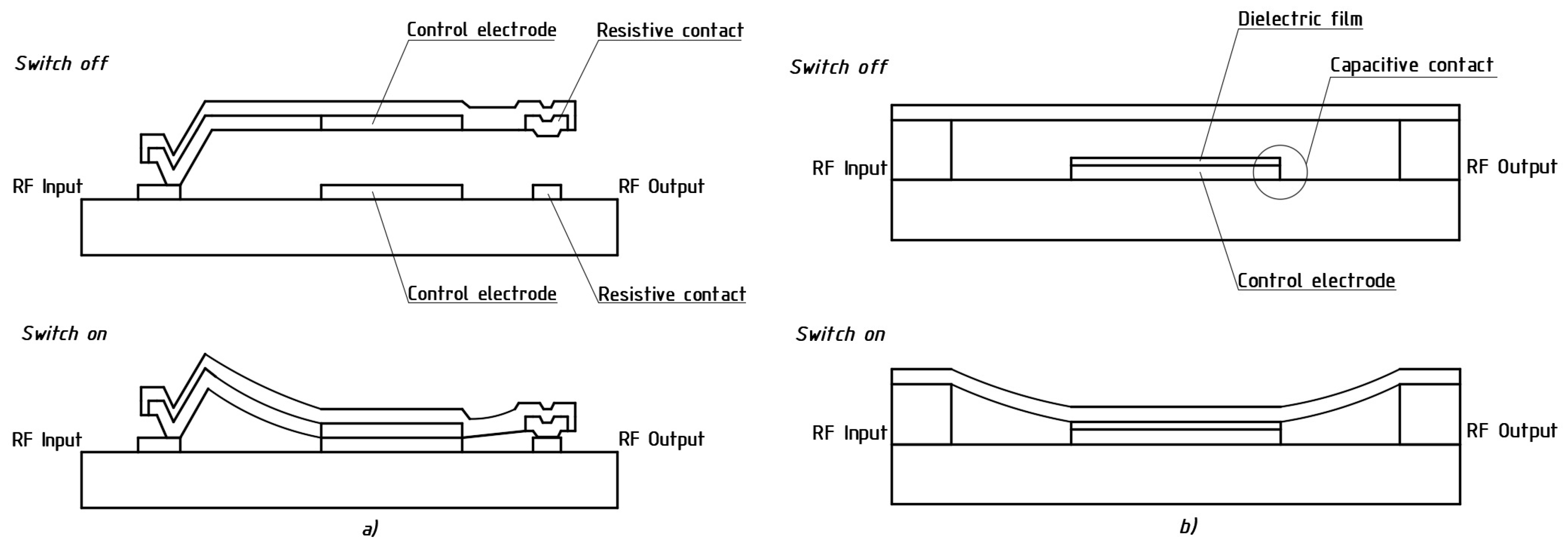
Microelectromechanical systems (MEMS) have achieved tremendous success since their introduction in the 1960s in the form of resonant gate transistors. The development of MEMS technology has led to the emergence of two new devices’ classes—microsensors and microactuators—which continue to replace their macro-scale counterparts due to their miniature size, low cost, low power consumption, and possible integration with semiconductor integrated circuit (IC) technology. However, radio-frequency (RF) electronic equipment has always needed switches that make low losses in the open state and provide high isolation in the closed state, with high permissible signal power, and low control power.
The first switch to fully meet the requirements of steel electromagnetic relays. After many years of improvement, modern RF electromagnetic relays provide low signal loss and high isolation in the off state, but they have such disadvantages as large size, high cost, and limited life. Their life expectancy is a minimum of about
switching operations with resistive load (which is greatly reduced with inductive load) and mechanical of the order of one
, and in some cases
and
switching operations. In addition, the lifetime of electromagnetic relays is influenced by a wide range of factors, along with shock and vibration loads [
1].
Switches on PIN-diodes and field-effect transistors (FET) based on GaAs have a number of advantages over electromagnetic relays, which are high-speed operation, small size and weight, as well as low power control. But they are characterized by higher insertion losses (for most applications > 0.4 dB) and for this reason in a number of applications can not replace electromechanical switches. The further development of RF electronics and the expansion of applications has led to the search for a new technology that can combine the advantages of semiconductor and relay switches. Such technology is the technology of microelectromechanical systems.
The first reports of MEMS switches developed specifically for RF applications date back to the early 1990s [
2,
3,
4,
5,
6,
7,
8,
9]. Recently, several micromechanical switches have been manufactured using MEMS technologies. For example,
Table 1 shows examples of typical designs, development, and characteristics of RF MEMS switches.
The transition to micro-scale RF MEMS switches is reflected in the significant growth of the market of RF MEMS segment and its applications. According to market research and technology analysis conducted by Yole Development Group [
15], the projected average annual rate of profit growth of the RF segment of MEMS devices is 10% per year, i.e., from
$2.3 billion in 2018 to
$4.4 billion in 2024. This exceeds the average annual rate of profit growth from the largest segments of MEMS devices such as inertial sensors, pressure sensors, microphones, and optical MEMS devices. At the same time, among the variety of RF MEMS devices (resonators, filters, phase shifters, oscillators), the greatest growth is marked by RF MEMS switches. Among the main areas of application of RF MEMS switches are telecommunications (base stations, smart cells for 5G reconfigurable antenna), industry (in automated instrumentation and test equipment), aerospace engineering (redundant matrix, commutation matrix, radars, and communications), in mobile communication devices and smartphones (BAW filters and duplexers, RF switches (antenna), antenna tuners). This expansion of RF MEMS devices is due to the successful transition of these technical and technological solutions from the research sector to the commercial one. However, in many applications, particularly in defense radar systems and industrial equipment, these devices are subject to adverse and frequently changing environmental conditions that can adversely affect their performance and the reliability of the system as a whole, as well as hinder the transition from research prototypes to commercial products.
In MEMS devices, in particular in RF MEMS switches, more significant in comparison with integrated circuits is the negative impact of the environment on the design of the switching element. Such negative environmental impacts include mechanical shocks, vibrations, external accelerations, and noise. Mechanically induced vibrations and shocks experienced by RF MEMS switch design elements can affect reliability and contribute to reduced performance, as well as cause structural damage. About these negative mechanical effects of the environment reported in a number of experimental studies [
16,
17,
18,
19,
20,
21,
22,
23,
24,
25,
26]. Mechanical shocks and high accelerations can exert heavy dynamic loads on structural elements. This can lead to the formation of cracks, chips or their complete destruction due to their strong movement. As a result, this leads to mechanical or electrical failure. Mechanical shocks can cause the microstructures of RF MEMS switches, such as suspended membranes or cantilevers fixed at one end, to hit the fixed lower electrodes located below them, causing stiction [
27] and short-circuit problems [
17], and therefore failure of the device. It is known that vibrations lead to a decrease in the performance of the device, while shock loads can lead to irreversible structural damage, while these mechanical loads are difficult to control electronically [
28], and can ultimately reduce the life of the device [
16,
17]. Also, external mechanical influences that cause the vibration of the switching element of the structure, while creating an instantaneous change in the resonant frequency. This change in the resonant frequency can lead to distortion of the RF signal by introducing unwanted amplitude and phase modulation of the RF signal passing through the RF transmission line [
29]. The performance of RF MEMS switches may be limited by the influence of noise due to their small size and the influence of electronic and mechanical parts. Therefore, there is considerable interest in the development of technologies to protect MEMS devices, and in particular RF MEMS switches, from mechanical vibrations, and shocks. A lot of efforts, especially in the case of MEMS devices, have already been devoted to the development of technologies for protection against mechanical effects of the environment [
16,
17,
30,
31,
32]. This protection is becoming increasingly important for high-performance devices or devices designed to operate in harsh environments. High-performance devices often contain sensitive structural elements and/or sensitive electronics that are highly sensitive to mechanical stress. Devices in harsh environments also require greater reliability than devices used in normal environments.
In this regard, in order to ensure the continuous growth and further commercialization of RF MEMS switches, the main purpose of this review is, firstly, to classify and review the main mechanical effects that affect the performance and reliability of RF MEMS switches, and secondly, the analysis of the mathematical apparatus that allows us to describe these mechanical effects. Thirdly, the analysis and review of modern methods and methods to reduce the negative impact of these mechanical effects on the design of RF MEMS switches.
3. Mechanical Destabilizing Effects
3.1. Vibrations
External vibrations affect the sealing cover of RF MEMS switches and cause mechanical loads in the structural elements. The reaction of the structural elements to the vibrations are transmitted in turn to the substrate RF MEMS switches. In this case, the forces acting on the structural elements will be the greatest and can even be destructive.
Large oscillation amplitudes produce harsh environments, especially those associated with flight and launch of spacecraft or in military equipment. While a spacecraft in orbit experiences very small low frequency (<3 Hz) oscillations, it may experience large oscillations in a large frequency band (up to 10 kHz) during launch. Military applications, including launching and flying missiles, similarly cause very large vibrations and large bandwidths (e.g., up to 50 kHz).
Table 2 and
Table 3 show the vibration frequency bands depending on the application.
Vibration can be periodic and random. In turn, periodic vibration can be harmonic and polyharmonic, and random vibration can be stationary, non-stationary, narrow-band and broadband [
45].
Figure 3 shows the classification of vibrations.
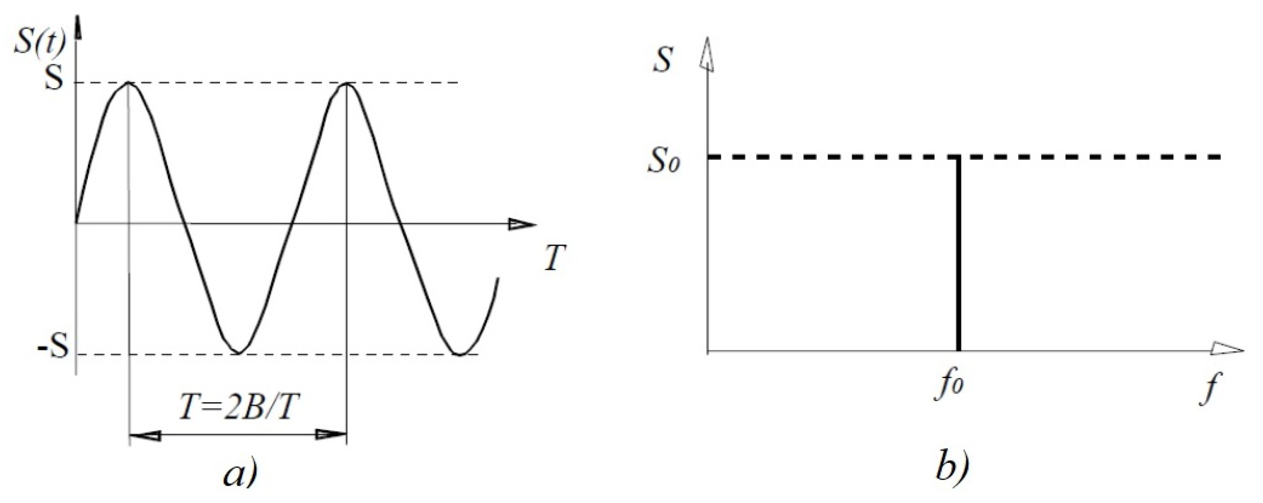
Harmonic vibration, the graph of which is shown in
Figure 4a, is rarely found in real operating conditions, but is widely used in laboratory analysis and testing. It is also important in determining the dynamic characteristics of MEMS structures of devices that are used to find the reaction of the system in more complex forms of vibration.
Vibration displacement at harmonic vibration is described by the Equation (
1):
where
S is the amplitude of the vibration;
is the angular frequency;
t is the time;
is the initial phase of oscillations.
Vibration velocity and acceleration is determined by Equations (2) and (3) by successive differentiation of Equation (
1):
where
is the amplitude of the vibration velocity;
is the amplitude of vibroacceleration.
Comparing Equations (1)–(3) it can be concluded that the acceleration is ahead of the phase displacement by
at sinusoidal oscillations. Since Equation (
4), called the Euler equation, also describes the harmonic oscillations with the angular frequency omega, to describe the harmonic vibration is often used a complex form of recording, determined by the Equation (
5):
Thus the main characteristics of the harmonic vibration are the amplitude of the vibration displacement, amplitude of vibration velocity, vibration acceleration amplitude, and the angular frequency of oscillation.
Harmonic vibration is often characterized by the vibration overload coefficient determined by the Equation (
6):
where
f—the frequency of harmonic oscillations.
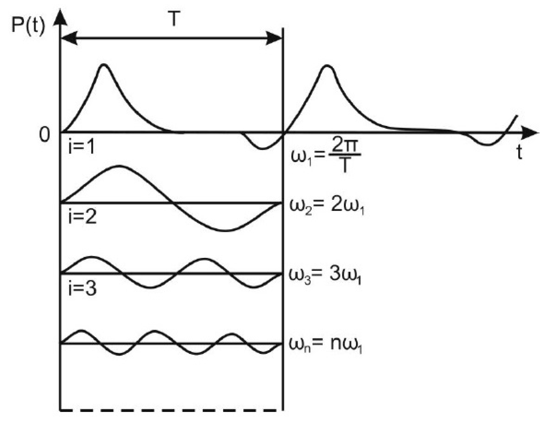
Polyharmonic vibrations create an electromechanical device having an unbalanced rotating mass. This vibration, as shown in
Figure 5, can be decomposed into the sum of harmonic components.
Analytically, this decomposition can be represented by the Fourier series using the Equation (
7):
where
,
—the basic frequency corresponding to the period of change of the disturbing force.
The coefficients of expansion
and
are determined by known Equations (8) and (9) and represent the amplitudes of the cosine and sine components of each of these harmonics:
The amplitude
and the initial phase
of each
i-the harmonic with frequency
is determined by using Equations (10) and (11) respectively:
The coefficient corresponds to the average value of the periodic exciting force P(t).
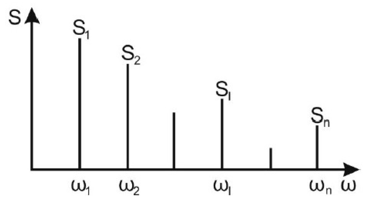
The set of frequencies
arranged in ascending order is called the frequency spectrum, and the set of amplitudes
—the amplitude spectrum of the periodic perturbation, as shown in
Figure 6.
Vibration, the parameters of which (vibration amplitude, frequency, etc.) change in time randomly is called random. It can be stationary and non-stationary. In stationary vibration, the expectation of vibration displacement is zero, the expectation of vibration velocity and acceleration are constant, the correlation function does not depend on the start of the reference. In non-stationary vibration constancy of static characteristics is not observed. This type of vibration can be attributed to the movement of vehicles when the jet engines.
The most dangerous is broadband vibration, because it leads to resonance oscillations in the moving elements of the RF MEMS switches. Thus, vibration acceleration increase tenfold, due to the presence of low stiffness in the direction perpendicular to their plane. The resonance frequencies of the moving elements of the design of RF MEMS switches can lead to three negative phenomena:
- (1)
the vibration acceleration amplitude at one or more points will exceed the permissible values specified in the technical conditions that is, the stability of the device will not be ensured;
- (2)
the resonant oscillations will lead to fatigue phenomena in the moving elements of the structure and, as a result, to a decrease in reliability and the number of switching cycles;
- (3)
the large acceleration at resonance of the moving elements of the design result due to changes in the characteristics of RF MEMS switches due to the emergence of vibration noise.
The Characteristic Features of Vibration on the Design of RF MEMS Switches
The design of RF MEMS switches should be vibration endurance and vibration strength. Vibration endurance determines the degree of sensitivity of structural elements to dynamic loads. It is characterized by the values of acceleration amplitudes and vibration frequencies, at which the normal operation of the device is not disturbed. In this case, the design of the RF MEMS switch must respond to vibration without generating a signal at the output, even in the absence of input exposure. Vibration strength determines the ability to withstand non-destructive long-term vibration loads. It is characterized by maximum amplitudes of accelerations, natural frequencies of RF MEMS design elements of switches, damping properties, and duration of vibration load.
RF MEMS switches are complex multi-element devices with a spectrum of static elastic characteristics. In addition, the structural elements have a different mass and, therefore, in general, the device can have a large number of natural frequencies. When coinciding with the frequencies of disturbing vibrations, natural frequencies can create a practically continuous spectrum of resonant frequencies of the device. Therefore, the probability of malfunction under the action of vibration will be proportional to the number of resonant frequencies in a given frequency range.
Permissible accelerations characterizing vibration endurance of RF MEMS design elements of switches in most cases are less than accelerations at which the vibration strength condition is fulfilled, and which should exceed the acceleration of the acting vibrations. Therefore, the design must be vibration strength and such that the accelerations experienced by the structural elements do not exceed the values that determine vibration endurance, i.e., the design must have damping properties.
Vibration acting on RF MEMS switches integrated into stationary electronic equipment. When integrating RF MEMS switches with stationary electronic equipment (which remains stationary during operation and, if necessary, can be transported by any means of transport to another location), vibrations acting on the electronic equipment during its operation and during transportation are distinguished. Vibrations in the operation of electronic equipment are excited by internal sources and, as a rule, have low levels of acceleration and fixed well-defined frequencies. Such sources of vibration can be fans, voltage converters, rotating antenna devices, generators of power sources. Internal sources of vibration must be determined on a case-by-case basis and vibration isolated. If each vibration source can not be vibration isolated, it is necessary to isolate from vibration the most sensitive elements of the RF MEMS switches. Internal vibrations, as a rule, affect only the vibration endurance of RF MEMS switches and almost do not affect their vibration strength. The amplitudes of accelerations and frequencies of such vibrations differ significantly from the vibrations acting on RF MEMS switches during transportation.
Vibration acting on RF MEMS switches integrated into electronic equipment installed on moving objects. In contrast to the stationary electronic equipment, which is subjected to transport vibration in the idle state, electronic equipment installed on mobile objects must operate reliably when the object is moving. In this case, electronic equipment may be subjected to more intense vibration than during transportation.
In general, radio–electronic equipment installed on moving objects is affected by stable and random vibrations. These vibrations act differently, so you should consider the effect of each of these vibrations and their simultaneous action.
The amplitude of vibrations of steady vibrations can be determined for any moment of time, whereas the amplitude of a random vibration can be determined only as the probability of its occurrence.
The correct determination of the parameters of the actual vibration is the main task in the design of RF MEMS switches installed on mobile objects. Excessive requirements and vibration parameters lead to an unreasonable increase in the rigidity and weight of the RF MEMS switches design and, as a result, to a decrease in their characteristics.
Mechanical fatigue of RF MEMS switch design elements under the influence of vibrations. In electronic equipment, in particular, RF MEMS switches as the main material of structural elements used metals with high conductivity, such as gold, aluminum, copper, nickel, platinum, etc. However, these materials are characterized by the number of cycles of variable loads for the entire period of operation than the number of cycles corresponding to the limit of endurance of the metal. Therefore, when calculating such structures for vibration strength, it is necessary to know the allowable stresses for limited endurance, which are determined on the basis of the fatigue curve. The fatigue curve graphically shows the relationship between the number of cycles
N at which a metal breaks down and the highest stresses
in the metal at that time. For an arbitrary point
M of the inclined section of the fatigue curve characterizing the area of limited endurance is obtained by the Equation (
12):
where
—the number of loading cycles corresponding to the inflection point of the fatigue curve;
R—the stress corresponding to the destruction of the metal under static load;
—the limit of long-term endurance of the metal;
—the number of loading cycles corresponding to the stress
;
—the stress in the limited endurance.
3.2. Shock
In addition to the vibration effects on the design of RF MEMS switches can have an impact and shock effects that occur during transportation or operation. During the impact on the structural elements of the RF MEMS switches, loads are applied for a short period of time
, resulting in acceleration of the structural elements, which can reach large values and cause damage. The intensity of the impact depends on the amplitude, shape, and duration of the shock pulse.
Table 4 and
Table 5 show the shock amplitudes depending on the application.
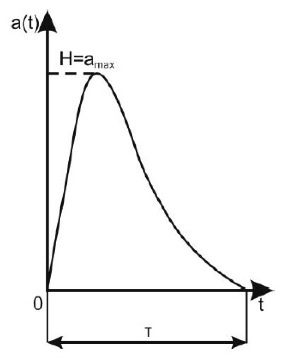
The form of the shock pulse is the dependence of the shock acceleration on time
a(
t), shown in
Figure 7.
When calculating the impact form of the shock pulse to simplify idealize, replacing it with a suitable simpler form: rectangular, triangular, semi-sinusoidal, as shown in
Figure 8. When replacing a real impulse with an idealized one, special attention is paid to the steepness of the front, since the “rigidity” of the shock depends on them. The amplitude of the pulse is the maximum value of the shock acceleration
A and the duration—the time interval of the pulse
. These three characteristics
,
A and
are usually given for the calculation of impact and design of protective equipment.
The mathematical model of the simplest forms of a shock pulse is described by the Equations (13)–(16):
Representation of shock pulses in the form of the simplest forms is justified not always. To more accurate results leads to the presentation of the shock the process in the form of the frequency spectrum
obtained by conversion Fourier, using Equation (
17):
After the shock, there are vibrations that can get into resonance with their own vibrations of the RF MEMS switches design elements. These resonant vibrations in form and characteristics are identical with resonant vibrations caused by vibration, and their elimination or reduction to an acceptable level is also one of the most important tasks of MEMS device developers.
3.3. Linear Acceleration
The effect of linear accelerations on the design of RF MEMS switches is typical for all types of devices moving at variable speed (during acceleration, braking). The effect of linear accelerations on the structural elements of RF MEMS switches is due to inertial forces, which can be many times greater than the gravitational force, the electrostatic interaction force, etc.
When the object moves along a curved trajectory (for example, along an arc of a circle of radius
R), the elements of the RF MEMS switches design will experience centrifugal acceleration determined by the Equation (
18):
where
—the angular and
V—the linear velocity of the object.
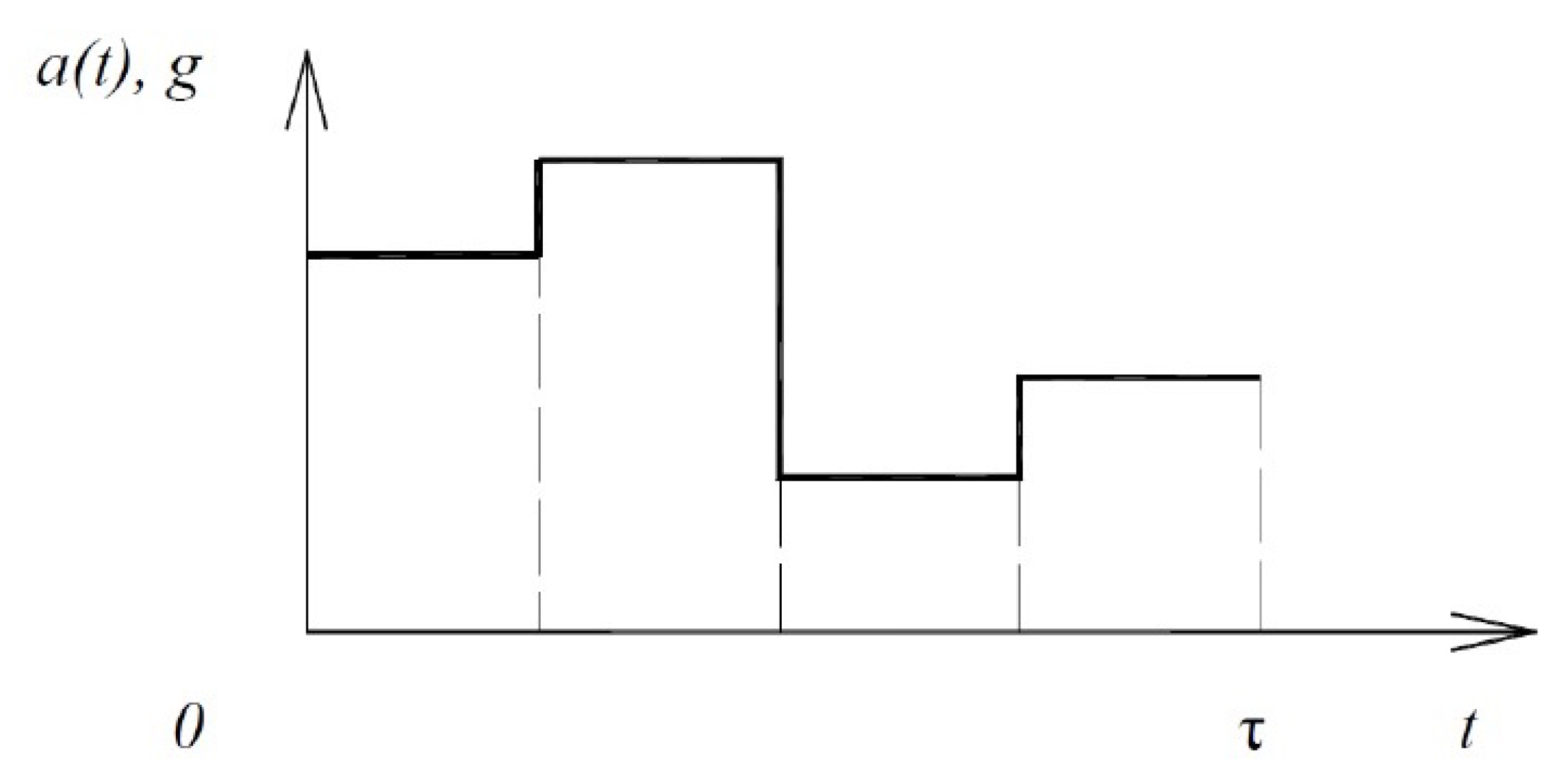
In technical MEMS devices often set the law, the changes in acceleration in time
and the duration of its action
is a step function, as shown in
Figure 9. The ratio of the current acceleration to the acceleration of gravity is called overload:
.
The difficulty in dealing with the influence of linear overloads is that they are virtually non-exclusive. Only in case of short-term action of linear overloads, some constructive measures of protection can be used. In all other cases, the performance can be achieved only by increasing the stiffness or strength of the elastic elements of the suspension and the structural elements of RF MEMS switches, which leads to an increase in its mass. Since the load for the elements are the forces of inertia, the increase in their strength can be achieved through the use of materials with a higher ratio , where —the allowable stress, —the density.
3.4. Acoustic Noise
Acoustic noise is characterized by a spectrum of sound frequencies, sound pressure, sound power, power of sound source oscillations. Acoustic noise exposes mechanical loads almost equally to all structural elements of RF MEMS switches.
The elimination of such vibrations of RF MEMS switches design elements or their reduction to the permissible level is one of the important tasks used in the conditions of vibration.
Other things being equal, the effect of acoustic noise is more destructive than the effect of shock and vibration loads. It leads to the instability of the RF MEMS switch design elements due to the appearance of vibration noises, which greatly contribute to the increase in mechanical loads.
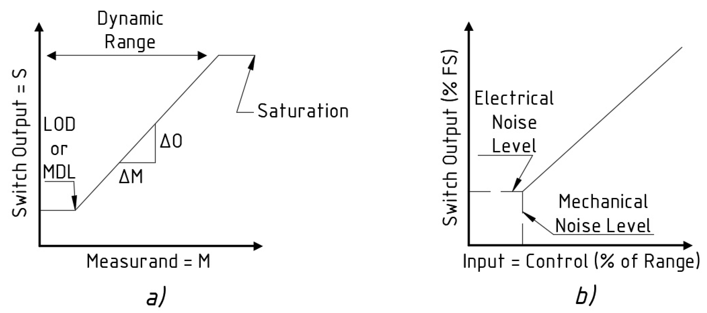
In general, noise includes both the unavoidable noise inherent in any electronic system and external noise, which can be reduced by shielding and other means. The problems caused by noise are well known. They fall into two categories. The first is a decrease in the performance of electronic devices, reducing the accuracy of information output. The second problem is related to the deterioration or limitation of the signal at the output of the electronic device. Almost all such systems have a calibration curve, as shown in
Figure 10. The calibration curves relate that is measured, the measured value
M, to the signal
S from the sensor or system. The slope
is the sensitivity of the sensor. Noise limits the small value of the measured value, which can be reliably determined. Thus, the noise determines the minimum detectable ‘limit of detection’ the measured value (LOD) for some specific measurement situation [
54].
Much attention is paid to LOD analytical and measuring radio–electronic systems. Sometimes LOD simply takes the value of the measured value at which the average signal is above the average noise value. Here is the standard deviation of the distribution of noise values obtained over time. Alternatively, ‘receiver operating characteristics’, called ROC curves, are used to pinpoint the exact but more complex tradeoffs associated with the definition of LOD. ROC curves allow you to rationally select the number of false positives that can be allowed for a given situation and sensor system.
Noise can limit the information at the output of electronic devices at low values of input (control) signals, as shown in
Figure 10. The control curves refer to the electrical input signal, which varies in some range with a mechanical output signal scale of 100% of the input value. For MEMS devices the measurement is most often stable, however, for MEMS actuators performance can be limited by the electrical noise of the input signal or mechanical noise output. Problems can be particularly acute for RF MEMS switches due to the relatively small size of these devices and their electronic and mechanical part
3.5. Other Noise Sources
Noise has many values, and therefore it is necessary to determine the type of noise of interest to RF MEMS switches. In components such as MEMS and in electronic systems containing them, there are two fundamental sources of noise: external and internal.
Noise from outside MEMS devices due to the influence of electromagnetic fields or mechanical movement, in particular sound, and vibration, may limit the performance of electronic systems. The magnitude of the external noise signals associated with the MEMS device is measured depending on the environment, and also depends on the sealing and installation method.
However, it is the internal noise sources in MEMS devices that impose strict restrictions on their performance. Reducing internal noise inherent MEMS devices is an important task in the design.
Fundamental causes of noise. The first is the detail of matter and energy in devices. Photons, electrons, atoms, molecules are all quanta. Their existence inside the devices or the impact on them is inevitably discrete. The second reason for the appearance of noise is the inevitable static variations of energies and movements of a large number of corresponding quanta. In large systems, the discrete and static nature of the presence and motion of energy and matter is often negligible. As the size of the systems decreases, the signals tend to decrease and the noise, in turn, tends to increase in relative scales. Together, this shows a double effect on the signal-to-noise ratio (SNR).
There is one noise mechanism that affects most types of MEMS devices, namely shot noise. This is due to the quantized nature of the signals MEMS material. The noise of the shot is caused by variable (random) arrival times of electrons or photons or necessarily by discrete movements of atoms or molecules inside or on the MEMS device.
Electronic noise is most important in RF MEMS switches because of the unavoidable electronic nature. There are several electronic noise mechanisms that have received the most attention from researchers:
- –
Thermal (Johnson or Nyquist) noise due to temperature fluctuations in carrier densities, as well as the movements of atoms and molecules;
- –
Noise of generation-recombination caused by random formation and annihilation of electron-hole pairs in semiconductors. It can also appear after ionization due to the absorption of energy quanta;
- –
Flicker noise (rattle), which is measured inversely to the frequency and is due to the variable capture and release of charge carriers in any conductors. Various types of flicker noise occurring in a variety of systems of widely varying nature of the system.
Mechanical noises, such as acoustics and vibrations, are usually caused by external sources, but there is one fundamental internal mechanical mechanism of noise, namely Brownian motion. This is due to dynamic unbalanced forces caused by random impacts of molecules on a small particle or structure. Also, this mechanism is called ‘random walk of noise’. Brownian motion becomes more significant as the size of the structure decreases. Adsorption-desorption noise is closely related to Brownian motion. This is due to the random arrival and departure of individual atoms and molecules on the surface of the MEMS device. Adsorption-desorption noise implies some non-zero arrival time of particles on the surface, in contrast to the transient effects that cause Brownian motion.
In the radio frequency domain, the ideal wave will look like an infinitely thin line in the frequency spectrum. However, a typical wave will have changes in the form of skirts that roughly follow the
distribution for frequencies relative to the wave. These skirts are the envelope of the sidebands due to the modulation of the wave and are inherently random in both frequency and amplitude, and are caused by various phenomena related to the physics of a particular oscillator. They are commonly referred to as phase noise. Phase noise is typically expressed in
units at different offsets from the carrier frequency. dBc—the noise intensity relative to the carrier force (tension). Phase noise can be measured and expressed as SSB (single sideband) and DSB (double sideband) values. Works containing expressions for calculating the contributions from various noise mechanisms in MEMS devices are limited to the following works [
55,
56,
57,
58,
59].
In addition, work [
60] reports noise associated with the mechanical deformation of the MEMS inductor. The device was manufactured using surface micro-processing technology. One of the problems associated with this approach and fabrication was in the suspension inductor or membrane supporting the inductor was susceptible to mechanical load. Therefore, in this study, an attempt is made to assess the change in electrical characteristics and the associated noise, which was caused by the physical deformation of the structure. A geometric model based on the manufactured inductor is developed. The noise caused by mechanical deformation was evaluated in three stages. Firstly, the deformation was calculated numerically as a function of mechanical loading. Secondly, the change in inductance was computed numerically as a function of displacement. Numerical simulation software was used to perform calculations at both stages. Finally, the noise power due to changes in the amplitude and phase of the RF signal is analytically calculated. From the data obtained, it was concluded that the amplitude of the noise signal can be equal to or greater than the thermal noise, depending on three factors, namely the system bandwidth, signal amplitude, and mechanical load.
In another work, the influence of Brownian noise, acceleration, acoustic noise, and power supply noise on the phase shifter (delay) circuit based on the switch was studied [
61]. The analysis was performed for capacitance-shunt and resistive switches. Several interesting observations were made about phase noise. Firstly, a well-designed switch has little phase noise from thermomechanical effects (Brownian noise). Phase noise was so low that it was difficult to measure even with the best equipment for measuring phase noise. However, it was also noted that low-impedance shunt switches and low-air-gap switches produce 20–40 dB higher phase noise. Secondly, the varactor phase shifters had a relatively high level of phase noise due to the tanks used in the construction. Thirdly, the distributed phase shifters had phase noise, which was about 20 dB lower than the varactor-based design, but still 20 dB higher than the switched network devices. Fourthly, the resistive switches had virtually no phase noise in the reflection mode, as their capacitance in the upper position was extremely low. In this paper, it is also concluded that the contributions of acceleration, acoustic noise to the bias voltage on phase shifters and RF MEMS switches were quite low. A similar approach in the following work was used to analyze the noise of RF MEMS switches, varactors and stop filters [
62]. Another article [
63] focuses on phase noise in oscillators based on microresonators with capacitive coupling.
In another study [
64], static phase noise and vibration sensitivity of a thin-film resonator (TFR) filter operating at frequencies of 640 and 2110 MHz were measured. [
65] this study provides an accurate simulation of phase noise in voltage control generator (VCO) circuits using numerical solutions of equations to calculate the capacitance of a MEMS capacitor. The phase noise was determined by combining the computed noise from the MEMS capacitor with nonlinear noise analysis at the circuit level. To provide accurate simulation, this capacitor model takes into account the influence of three noise sources: the generator phase noise, which consisted of electrical thermal noise,
noise, and mechanical thermal vibration noise.
Similar work on noise modeling of MEMS varactor is carried out in [
66]. Was represented by the mechanical noise exhibited by the MEMS varactor. It comes from the Brownian motion. Brownian motion is converted into noise current. Therefore, for the description of the conversion mechanism uses the model of the noise current, which was transformed into phase noise.
Noise resonator studies seem to have attracted the interest of many research groups. One study was conducted at Columbia University [
67] and the other by Stanford researchers [
68].
In general, phase noise is the dominant source of noise in RF MEMS devices from simple inductors and filters to complex systems such as voltage/current control generators (VCO). These noise components lead to a random change in the capacity of the switch, which leads to additional phase and amplitude noise at the output of the controlled MEMS generator or phase shifter.
3.5.1. Brownian Noise
These noise components lead to a random change in the capacitance of the RF MEMS switch, which in turn leads to additional phase and amplitude noise at the output of the RF transmission line. In this connection, a separate consideration of the effect of Brownian noise on RF MEMS switches is necessary.
The Brownian noise is due to the thermal energy accumulated in the mechanical structure with a constant stiffness
k, the damping coefficient
b and the mechanical resonance frequency
, with the Brownian noise component determined by the Equation (
19):
where
—the Boltzmann constant;
—the measure of quality of a MEMS structure;
—the mechanical resonance frequency;
m—the mass of the MEMS structure.
The force acting on the movable electrode RF MEMS switch, due to the influence of thermal noise is determined by the Equation (
20):
The damping factor b depends on the thickness of the moving electrode, the number of holes in it and the viscosity of the medium (usually air or nitrogen).
The damping coefficient also has a strong influence on the dynamic characteristics of RF MEMS switches. In practice, a well-designed switch has show quality Q within the following limits , so that the dynamic characteristics are limited only by the mechanical characteristics of the structure (mass, stiffness constant, etc.).
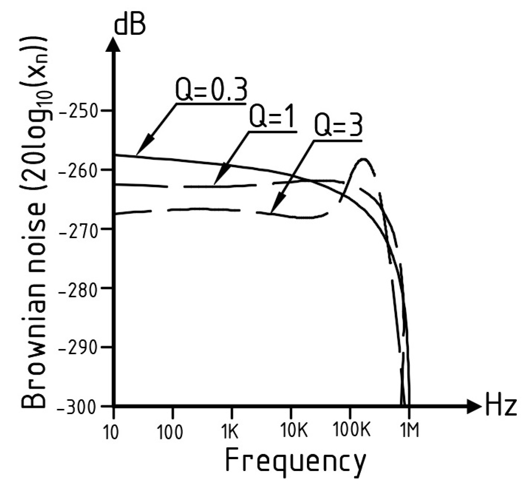
Thus, it can be seen that switches with a high stiffness coefficient of the structure and a low damping coefficient are characterized by a very low level of Brownian noise. For example, the Brownian noise of a movable switch electrode (membrane) with
N/m,
kHz,
K,
shown in
Figure 11.Adapted from [
69].
Brownian noise can be represented as the sum of sinusoidal signals with random amplitude and phase. A sine wave with a mechanical frequency
and an amplitude equal to the square root of the noise power in the frequency band 1 Hz around
is given by the Equation (
21):
3.5.2. The Effect of Brownian Noise on Capacitive RF MEMS Switches
As a capacitive RF MEMS switch can be a standard capacitive shunt RF MEMS switch developed by Raytheon with a central pull-down electrode [
70] or a shunt switch with two separate pull-down electrodes [
71,
72], as it can be a switch with a low coefficient of stiffness [
73]. It is important that in the case when the switching element of the structure, namely the movable membrane, is in the upper (initial) position, this allows the microwave energy to pass with very small insertion losses. In the case when the switching element of the structure is in the lower position, the signal coming to the RF input of the transmission line is shunted (closed) to the ground lines.
The capacity in the upper (initial) position of the switching element of the structure is determined by the Equation (
22):
where
—the fringing capacitance or parasitic capacitance;
—the variable capacitor with two parallel plates.
It is assumed that
, where
for shunt designs of RF MEMS switches. Taking into account Brownian noise, the capacitance of an alternating capacitor with two parallel plates can be determined using the Equation (
23):
where
—the component of Brownian noise motion of a moving structural element.
The capacitance in the upper position of the switching element of the structure taking into account the zero Brownian noise is determined by the Equation (
24):
where
– the capacitance in the upper position with zero Brownian noise.
The capacitance in the upper position leads to the dispersion of the microwave energy, determined by the Equation (
25):
where
—the RF transmission line impedance.
Phase noise. The phase
is the phase delay due to the capacitance in the upper position and is determined by the Equation (
26):
Using the Equation (
24), the phase delay with Brownian noise is determined by the Equation (
27):
If the RF signal is specified by the
distribution, then the RF output signal is determined by the Equation (
28):
Using Equation (
19) the RF output signal can be determined using the Equation (
29):
The power in each of the side bands relative to the carrier is an additional phase noise due to the switching element of the structure and is determined by the Equation (
30):
Four important points to consider when designing RF MEMS switches:
- (1)
the influence of the stiffness coefficient on the value of phase noise . If the stiffness coefficient decreases by 1 N/m, the phase noise increases by –160 dBc/Hz.
- (2)
strong dependence of phase noise on the air gap, and from the Equation (
30) it follows that the phase noise depends on the parameter
. For structures with a low coefficient of rigidity it is advisable to use sealing in a low-pressure environment (10–50 mtorr). This will significantly reduce the damping factor, which in turn will lead to much lower phase noise.
- (3)
the third point is that the phase noise is constant at low offset frequencies, and decreases rapidly after the mechanical resonance frequency (30–300 kHz depending on the design). However, for most radar applications, the end frequencies are between 5 and 100 kHz. Designing an RF MEMS switch design with a low mechanical resonance frequency will not necessarily result in improved performance, since these designs typically have a low stiffness coefficient, resulting in higher low-frequency phase noise. In addition, in this case, the dynamic characteristics are significantly reduced.
- (4)
The Equations (26) and (30) show that the phase noise depends on . However, this is not entirely true for narrowband systems. If the circuit is designed correctly, the same value must be selected at any operating frequency. In other words, at 60 GHz should be six times less than at 10 GHz. Therefore, the phase noise component is independent of the calculated frequency.
Amplitude noise. The value of
from Equation (
26) is determined by the Equation (
31):
The effect of Brownian noise on the RF output signal is determined by the Equation (
32):
Replacing
and
, using Equations (22) and (24) we obtain Equation (
33):
The power in each of the side bands relative to the carrier is an additional amplitude noise due to the switching element of the structure and is determined by the Equation (
34):
thus
.
3.5.3. The Effect of Brownian Noise Effects in Resistive RF MEMS Switches
Resistive RF MEMS switches are devoid of the influence of Brownian noise in the lower position of the switching element of the structure (cantilever), since the switch is fixed on the substrate. However, in the upper (initial) position, if the switch is used in phase filters, there is phase noise. The phase of reflection in resistive switches is determined by the Equation (
35):
In this case, when determining the
and
in accordance with Equations (21) and (24), the phase noise of the site with respect to the carrier corresponding to the reflection is determined by the Equation (
36):
It should be noted that = 2–6 pF and = 2–3 for most resistive RF MEMS switches, since most of the capacity in the upper position of the switching element of the design is due to the parasitic capacity between the parts of the RF transmission line. Thus, the phase noise of the resistive switch (in the reflection mode) is 100–300 times less than that of the shunt switch in the transmission mode.
4. Methods of Protection of RF MEMS Switches from Mechanical Destabilizing Effects
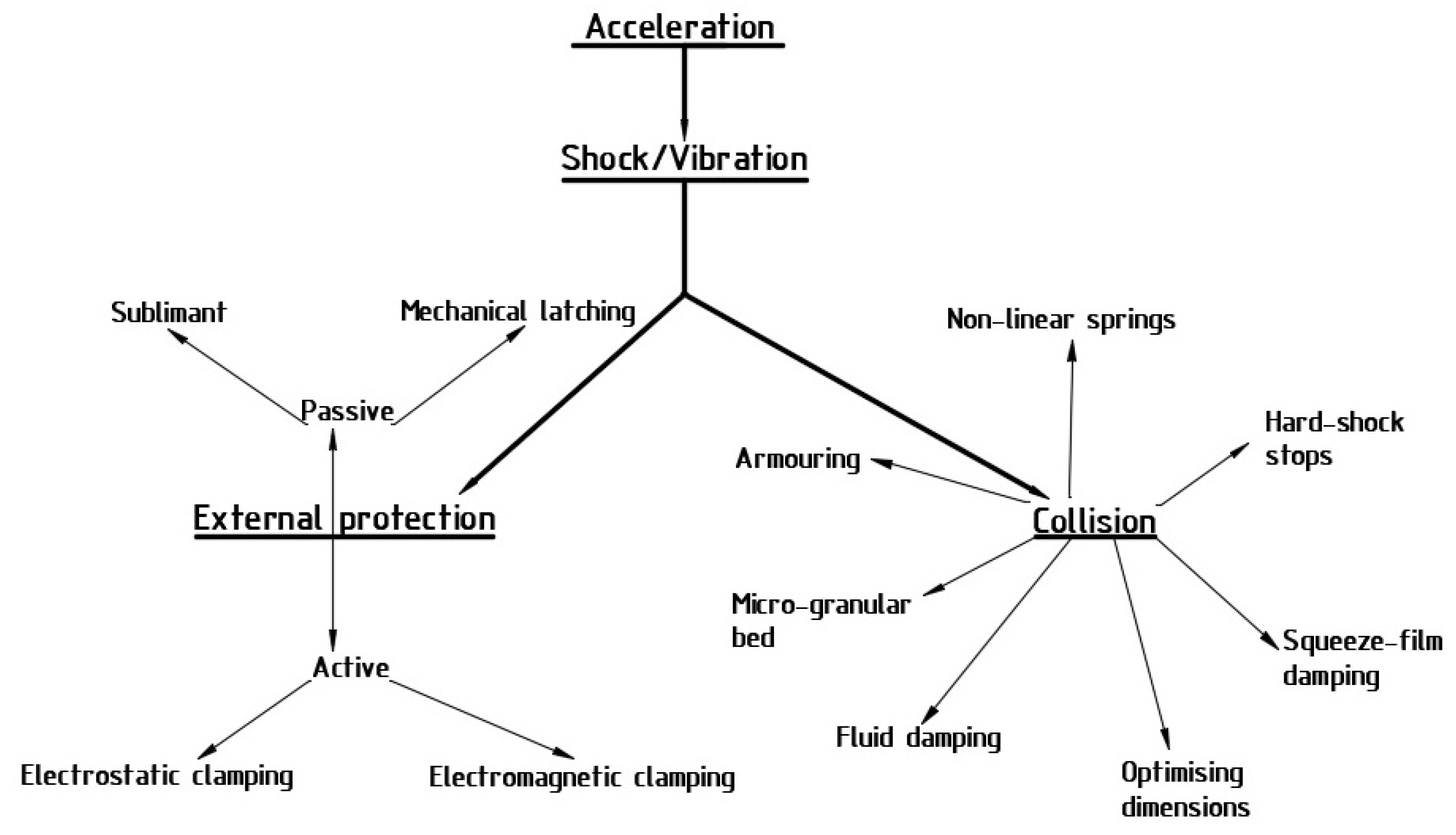
The numbers of methods presented in
Figure 12 are proposed as possible protection against mechanical destabilizing effects of RF MEMS switch design elements.
From the data of the diagram presented in
Figure 12, it follows that there are two directions that can be used for protection against mechanical destabilizing effects of RF MEMS switches: external protection or certain methods of collision prevention and control.
External protection measures include the use of a wax sublimate to prevent the movement of mechanical components during impact [
74], as well as mechanical fixation [
75], an electrostatic clamp [
76] and an electromagnetic clamp [
77] of the switching element of the RF MEMS design of switches. External protection can further be divided into two categories: active protection, where an external power source is required to maintain the clamp, and passive protection, where an external power source is not required [
78].
The advantage of using external protection is that the structural elements do not need to be reinforced, as any change can adversely affect the electromagnetic and dynamic characteristics and therefore it is better to avoid it. The electrostatic and electromagnetic clamps provide only a limited clamping force and both require an external power supply in case of impact. Mechanical clamping methods are also limited in their clamping force and, in the case of silicon fabrication, can potentially be destroyed. In addition, a necessary condition is that the structure must be released after the impact has ceased, which can be a problem if the clamp does not work in any way.
Internal protection measures include dimensional optimization, the using of a micro-granular base, damping of the compressible film, fluid damping, non-linear springs, rigid shock stops or metal reinforcement to dissipate the kinetic energy of the impact.
Size optimization. In the case of mechanical influences, structural failure can be minimized by optimizing the dimensions of the RF MEMS switch design in question so that the stresses do not exceed the tensile strength. [
79] it is shown that changing the size of some elements can minimize the effect of some known impact. However, the characteristics of the device can be reduced by the application of these protection measures, and it is applicable only in cases where the magnitude of the impact is known.
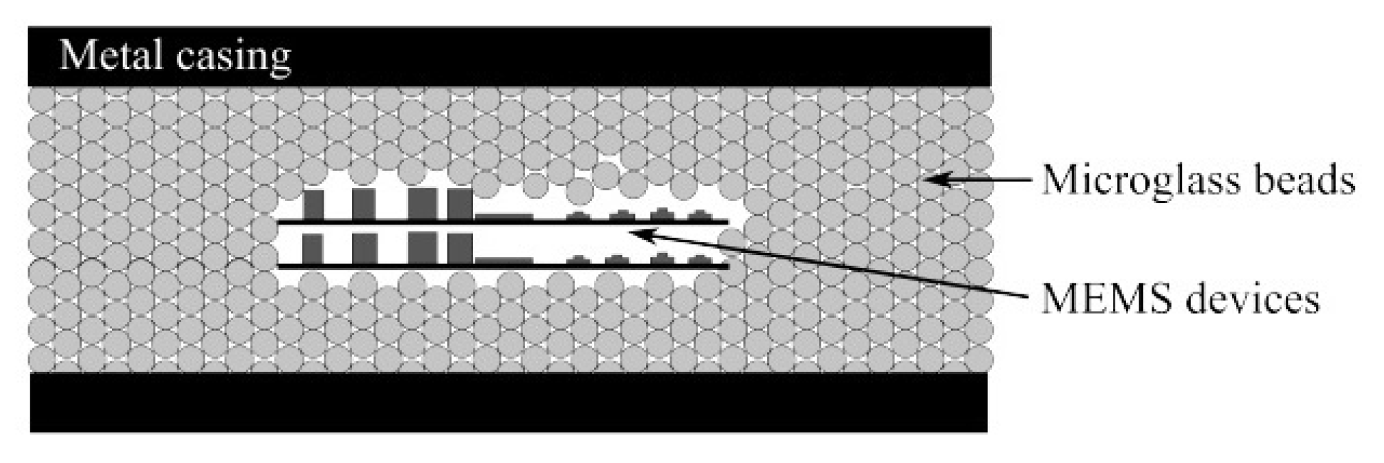
Layer of micro granules. [
80] a method of protection against high impact is presented, which uses a layer of micro-granules for military applications, as shown in
Figure 13. The densely packed layer of micro-granules finds inside the metal housing. Thus, the micro-granules reduce mechanical excitations transmitted to the structural elements, absorbing the kinetic energy of the applied impact.
However, if the normal operation of the MEMS device requires freedom of movement of structural elements, this method is not suitable.
Squeeze-film damping. In [
81] the influence of damping effect on the reduction of mechanical influences using a threshold accelerometer, which has a large perforated flat area at a short distance from the substrate, was investigated. Damping is increased by reducing the perforated holes. This minimizes out-of-plane movement of the microstructure, and thus reduces the likelihood of contact. However, as a method of protection against impact, it is very limited in its application and potential.
Fluid damping. Fluid dampers that dissipate energy through thermal and acoustic energy are generally too bulky to use in MEMS and are not suitable for harsh operating conditions [
80].
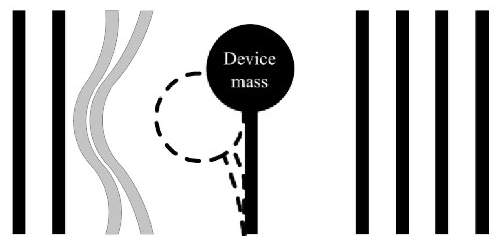
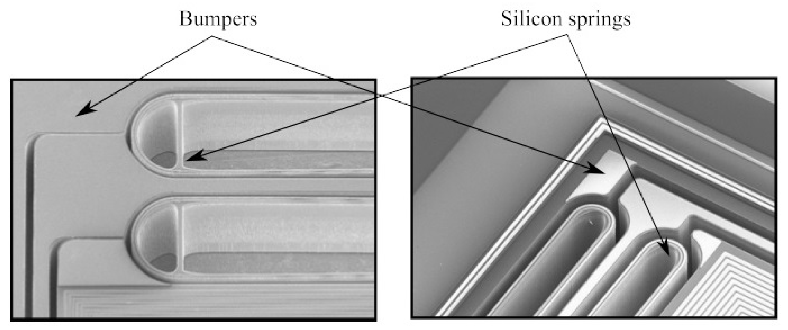
Nonlinear springs. [
82,
83] a compatible shock stop using non-linear springs has been created. This structure is achieved by adding elastic suspension elements in the form of beams, as shown in
Figure 14. However, due to the beams, a certain amount of kinetic energy is softened through the bend, but the movement of the sensitive mass increases, which requires an increase in the frame. In addition, the beams themselves are made of silicon and are therefore at risk of destruction and debris.
Hard shock stops. Rigid shock stops have been studied in [
84,
85] they are limited in protection due to the fact that they themselves can act as sources of the secondary shock and vibration effects. An example is included shock stops in the suspension design of the microseismometer, as shown in
Figure 15, to prevent compression and destruction of the sensitive mass by limiting its movement when applying force, but they are made of silicon, so they remain susceptible to destruction.
Metal reinforcement. The works [
82,
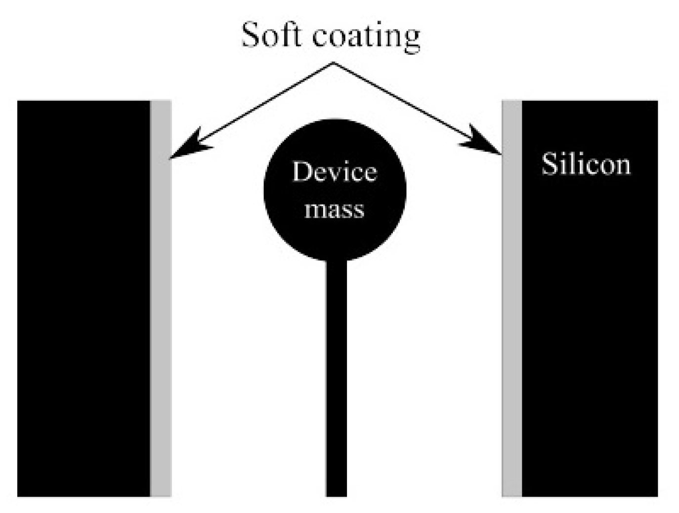
83] investigated the reinforcement of the colliding areas of the microstructure with thin layers of soft metal coatings, such as copper and gold, as shown in
Figure 16, which have lower reduction factors (
e) than the material of the microstructure. The recovery factor is the ratio of the velocities after and before the collision:
e = 0 for a completely inelastic material and
e = 1 for a completely elastic material. Although it is widely recognized that
e is not usually a constant value and depends on how the properties of the material, and an impact speed of [
86,
87,
88,
89,
90,
91], is defined
e = 0.7 for silicon and
e = 0.22 for copper and gold.
By using softer materials at the point of impact, the number of collisions is reduced, and the settling time of the system is reduced. In comparison with the non-laminated springs described by the same authors, the number of collisions is much less, and the mass of the sensing element of the structure is not increased.
It has been tested that at mechanical influences from 100 g to 2500 g, micro-stops of mechanical influences, as shown in
Figure 14 and
Figure 16, retained their design without permission in 4% of cases without shock protection, 88% when using non-linear springs, 94% when using a soft coating. For manufacturing, a parylene coating was used to create a soft coating [
83], and not the metal layers studied in the simulation [
82]. Parylene was chosen because of its chemical stability, the possibility of deposition at room temperature and conformal coating. The disadvantages of metal reinforcement include the fact that the deposition of side surfaces is a complex process, as well as the protective potential often depends on the thickness of the metal layer. Disadvantages of using parylene as the metal layer is to cover the entire design of the device, and not only in places of aprotinine or application of shock and vibration effects.
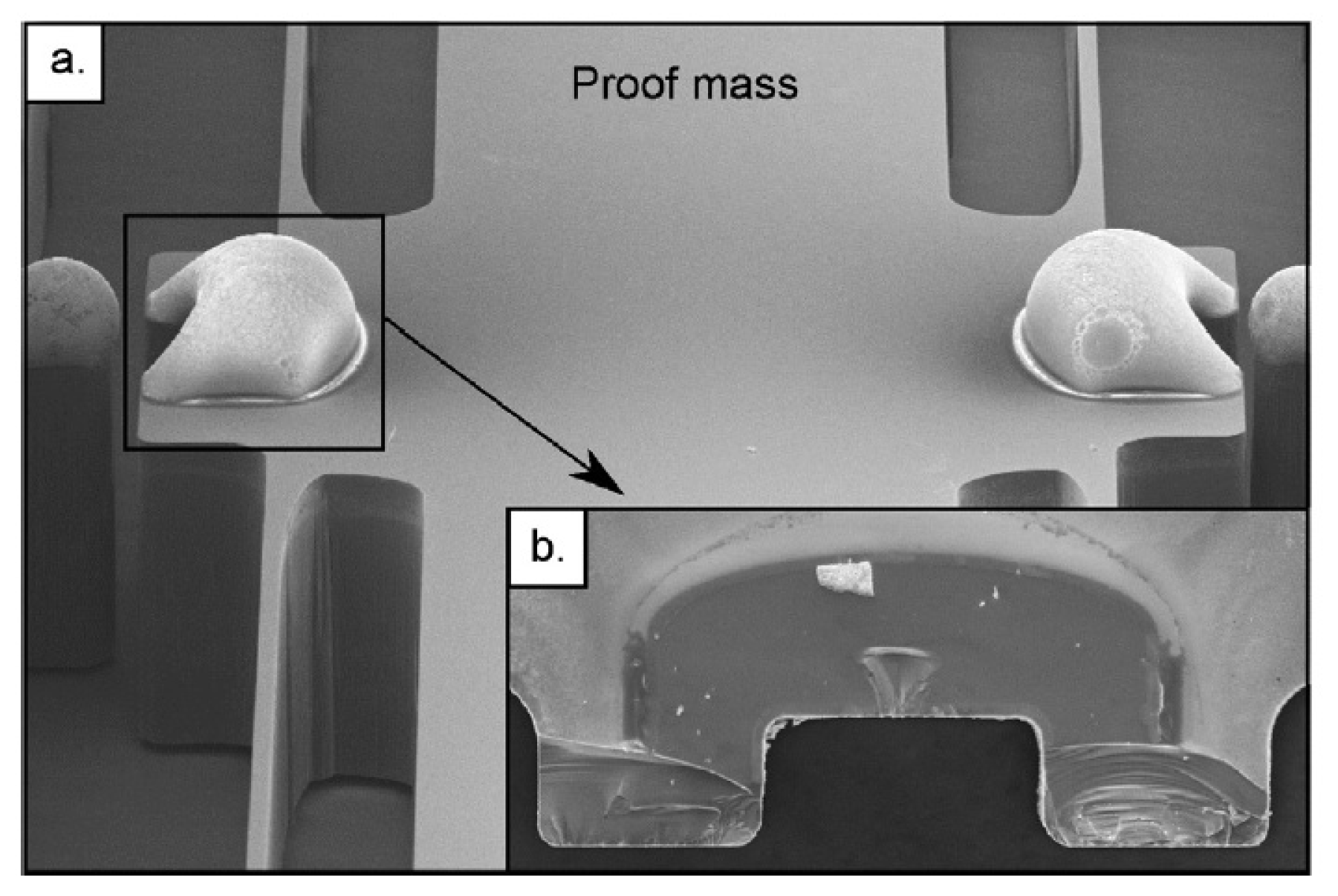
Solder as metal armor. A possible alternative is the use of solder in the form of metal armor, as shown in
Figure 17.
Solder, in this case, is a soft metal alloy, which is able to absorb large amounts and deform under impact. Solder also has the additional advantages that it is already widely used in the packaging of MEMS devices and is thus easily incorporated into the current manufacturing processes.
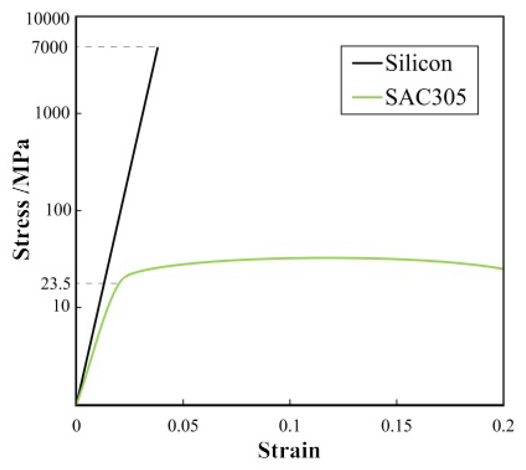
Table 6 shows the properties of lead-free solder Sn3.0Ag0.5 Cu and silicon, which is the main material of structural elements of most MEMS devices, and
Figure 18 shows the stress-strain curves. From the graph shown in
Figure 18, it is clear that the solder is much more malleable than silicon. When stress is applied, the solder continues to deform plastically at an almost constant rate, while silicon, on the contrary, has a higher final strength and, at a certain amount of stress and time, its mechanical destruction occurs because it has no plastic region.
After yield solder plastically deforms at a near-constant rate, while in contrast silicon has a so higher ultimate strength, but rather than yield a sudden brittle failure occurs; there is no plastic region.
5. Conclusions
RF MEMS switch is a device with a switch element suspended on the anchor areas by means of elastic suspension elements to achieve the closure or opening of an electric circuit. Mechanical instability, in this case, is used and controlled to switch between two stable states. However, despite the simplicity of this approach and the performance advantages, undesirable effects on the design of the switching element can lead to unstable behavior and distortion of the transmitted RF signal, and therefore to errors in the RF systems in which they are integrated.
The progress of research in the last decade in preventing and minimizing various undesirable effects has been very successful, especially with regard to the minimization and control of the dielectric layer charge, the effect of Brownian and other types of noise, the effects of spontaneous triggering when switching high power RF signals, the prediction of fatigue life, as well as the use of design solutions to improve temperature stability and ensure reliable and long-term contact. However, the full operation of these RF devices in wide commercial and military applications is limited by the impact of shock and vibration destabilizing effects on the design of the switching element.
In this regard, this review analyzes the relevant literature on the possible mechanical destabilizing effects on the design of the switching element, as well as the methods used to reduce their impact. Due to this, there was an understanding of the mechanisms of destabilizing effects. In addition, it was found that the reduction of the impact of shock and vibration effects is difficult to achieve only by the correct optimization of the switch design without the use of additional design methods.
Unlike external linear accelerations, vibrations, and noise, shock influence damage the structural elements of MEMS devices. Most shock protection techniques focus on limiting the displacement of moving structural elements so as to limit the maximum bending stress. One of the common methods to achieve this goal is the use of hard shock stops limiting movement. Despite their many advantages, hard shock stops can be a source of secondary shock and vibration, which in turn can lead to structural damage in some applications. Therefore, the use of shock protection based on nonlinear spring shock absorbers and shock stops with a soft coating is promising. Both technologies are compatible with microsystem manufacturing technology and can be integrated into many MEMS devices without major design changes.
Further research on this topic will be devoted to analytical and numerical modeling of mechanical characteristics of the structural methods of protection against shock and vibration. In particular, checking the effectiveness methods from strong shock and vibration effects of the environment by dissipating a large amount of energy through the nonlinear spring shock absorbers and shock stops with a soft coating.
