Article

A New High Voltage Gain DC to DC Converter with Low Voltage Stress for Energy Storage System Application

1
Department of Electrical Engineering, National Taiwan University of Science and Technology, No. 43, Keelung Rd., Sec.4, Da’an Dist., Taipei City 10607, Taiwan
2
Department of Electrical Engineering, ZHCET, Aligarh Muslim University, Aligarh, Uttar Pradesh 202002, India
3
Industrial Engineering Department, College of Engineering, King Saud University, P.O. Box 800, Riyadh 11421, Saudi Arabia
4
Department of Statistics and Operations Research, College of Science, King Saud University, P.O. Box 800, Riyadh 11421, Saudi Arabia
*
Author to whom correspondence should be addressed.
Electronics 2020, 9(12), 2067; https://doi.org/10.3390/electronics9122067
Submission received: 5 November 2020 / Revised: 27 November 2020 / Accepted: 30 November 2020 / Published: 4 December 2020
(This article belongs to the Section Power Electronics)

Abstract

:
Increasing energy demand globally has led to exploring ways of utilizing renewable resources for sustainable development. More recently, the integration of renewable distributed resources in small- and large-scale grid has been seriously researched. Development in renewable power sources and its integration with the grid require voltage level conversion to match the grid/micro-grid level. The voltage level conversion is brought about by employing Direct Current-Direct Current (DC-DC) converters with boosting features. The paper presents a wide gain range DC-DC boost converter with a low-stress on switching devices. The proposed converter’s voltage gain is high compared with the conventional quadratic boost converter and other recently developed high gain boost converters. The topology has been compared with recently proposed topologies, and comparative analysis based on various performance parameters has shown that the topology is suitable for renewable and sustainable energy storage and grid integration. The power loss analysis has been done by incorporating the switching and conduction losses. A hardware prototype of 150 W has been developed to validate the converter’s performance in steady-state as well as in dynamic conditions.

1. Introduction

DC-DC converter works on the principle of energy transfer between energy storage elements. By controlling this transfer of energy in one complete cycle, constant and high voltage can be obtained at the output. Conventional boost converter uses a single inductor and capacitor to obtain high voltage at the output. Other variants such as Cuk converters, Single Ended Primary Inductor Converters (SEPIC), and ZETA converters are also being developed to get high DC voltage output. These converters have a simple structure, but the voltage gain is limited [1]. Moreover, the stress across the switching devices is high, and efficiency is low. The converter cannot be operated at very high duty ratios as the conduction losses become elevated due to parasitic resistances and voltage gain decreases. Due to these problems, high gain DC-DC converters employing more than one inductor, and multiple capacitors can be employed to increase the converter’s gain [2].
High gain DC-DC converters have increasingly become popular due to their suitability in solar Photovoltaic (PV) systems and electric vehicles. The output voltage from solar PV modules, fuel cells, and batteries is generally low and needs to be boosted up to maintain the DC-link voltage at the inverter’s input [3]. The power flow in DC-DC converters can be unidirectional or bidirectional. Isolated topologies are suitable for high power applications and where efficiency required is high. Non-isolated topologies are usually used in low and [4] medium power applications where efficiency and electromagnetic interference are not significant concerns. Several isolated and non-isolated topologies use voltage multiplier cells (VMC) made up of switched inductors and capacitors to increase the converter’s output voltage. In some topologies, a coupled inductor is also used in VMC to increase the gain of the converter. Another advantage of using VMC is that a high output voltage can be obtained at lower duty ratios [5].
Multilevel DC-DC structures use multiple switched capacitors [6] at the output stage to boost the output voltage. Authors have proposed a novel buck-boost and boost converters with continuous input current in [7] and [8], but the voltage gain is limited at higher duty ratios. A single switch modified SEPIC converter with a high voltage gain, and low voltage stress is proposed in [9]. Switched inductor topologies have an advantage that peak transient current through the switch is avoided as the capacitor is not charged directly through the source. The input current is also continuous if the inductor is on the input side. However, the gain is less as compared to the switched capacitor topology. The use of many inductors increases the weight and size of the circuit. Whereas multiple switched capacitors can easily enhance the converter’s voltage gain substantially [10,11,12]. Switched capacitors, when employed with DC-DC converters, increase the gain of the converter substantially but the high charging current decreases the efficiency of the converter. In steady-state, the capacitors are in series and transfer their energy to load. Inductors are charged in the ON cycle, and during the OFF mode, the inductor discharges [13], and capacitors are charged in parallel. A new buck-boost converter with continuous input current with a quadratic gain is proposed [14].
Coupled inductor topologies have a high voltage gain, higher efficiency, and reduced voltage and current stresses across switches. The problem with coupled inductor topologies is that energy trapped in the leakage inductance needs to be recycled to avoid voltage transients across the switch and increase the circuit’s overall efficiency. For this, an additional clamped circuit needs to be designed for these topologies [15,16,17,18], which increases the circuit’s complexity. A new triple mode converter is proposed in [19], but many switches and inductors are required to obtain high voltage gain. The converter in [20] uses a Cockcroft-Walton based VMC to increase the gain of the converter. A new converter boost converter with VMC with switched capacitors is presented. The topology uses only a single inductor with switched capacitors, but the voltage gain [21] is limited. At lower duty ratios, the gain is little. Interleaved boost converters are characterized by a low ripple in current and low stress across the switches but require multiple VMCs (Voltage Doublers, Dickson Cells) at the output to boost the voltage.
Researchers have made efforts to optimize the number of VMCs to be used at the output so that a smaller number of components are required [22,23,24]. Another family of the DC-DC converter is quasi z source converters. The input current for these converters is continuous, and the stress across switching devices and capacitors are low. However, these converters have limited voltage gain [25], [26], and cannot be operated at higher duty ratios. The DC-DC converter performance with non-ideal components is discussed in [27]. It is shown that at low input voltages and high duty ratios, the converter performance deteriorates. The voltage gain and efficiency both decreases substantially. Some other new and efficient topologies of the DC-DC converter with high gain is discussed in [28] and [29]. Quadratic boost topologies have the advantage that very high gain ratios can be obtained at [30] low duty ratios. Low duty ratio operation reduces the stress across devices and improves the efficiency of the converter. Quadratic boost converters (QBC) generally use switched inductors and capacitors to increase the converter’s gain. Non-isolated QBC provides high gain with reduced stress on switches but at the cost of reducing the efficiency at higher duty ratios efficiency [31,32,33]. The advantages of non-isolated QBC over other topologies makes it a suitable choice for low and medium power applications [34,35]. The DC power supply can be given to a high gain converter and can be used even for a DC-AC high conversion application [36,37]. The switched capacitor application has also been discussed in [38,39,40,41].
This work’s motivation and objective is to develop a new quadratic boost converter with voltage multiplier cells. The proposed converter’s performance is an improvement over conventional QBC (CQBC) and other recently developed topologies. The voltage gain of the proposed converter is much higher than the conventional boost and CQBC. Along with low voltage stress across all components, the proposed converter’s input current is also continuous, which is another desired feature of the proposed converter. The converters utilize only two inductors with the same gate signal to generate a high output voltage. The converter has a simple structure, and its control is easy. The convertor performance is analysed in an open loop structure, and the converter’s working in CCM is shown in Section 2. Voltage stress and design of passive components are shown in Section 3. A comparison of the proposed converter with other topologies is discussed in Section 4. The simulation and experimental results along with efficiency calculation discussed in Section 5 and Section 6, respectively. The working of the proposed converter in dynamic conditions is discussed in Section 7. Discussion and conclusion are in Section 8 and Section 9, respectively.

2. Proposed Topology

The conventional quadratic boost converter has one switch. The switch is connected across the load and hence has to bear the voltage stress equal to the output voltage (Vo). It utilizes two inductors, but the voltage gain remains limited.
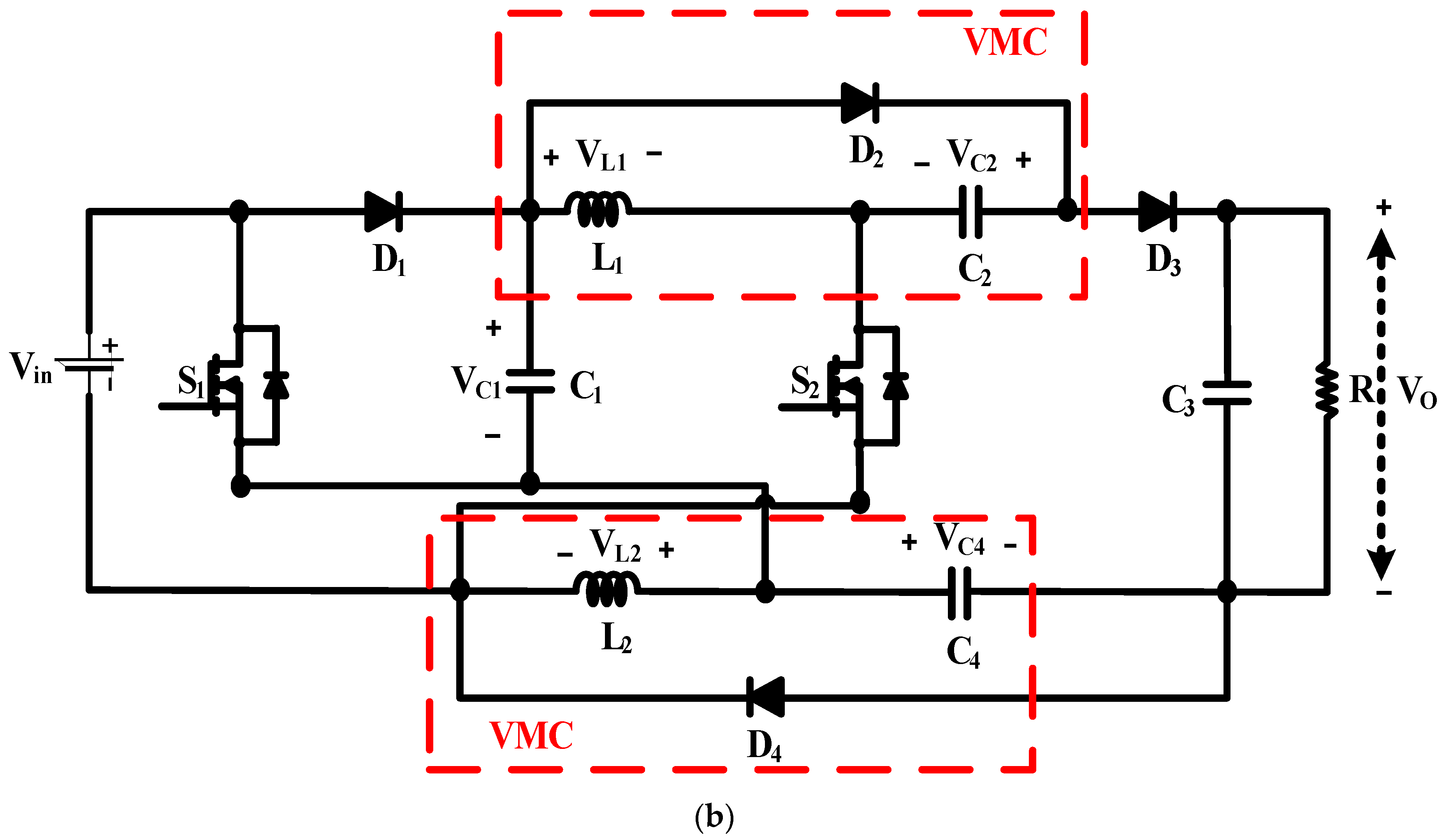
The Proposed converter topology is shown in Figure 1. It has six passive components, namely two inductors and four capacitors. The proposed converter comprises two voltage multiplier cells (VMC), as shown in Figure 1. These VMCs are used to improve the voltage gain further and reduce the voltage stress on the switching components.
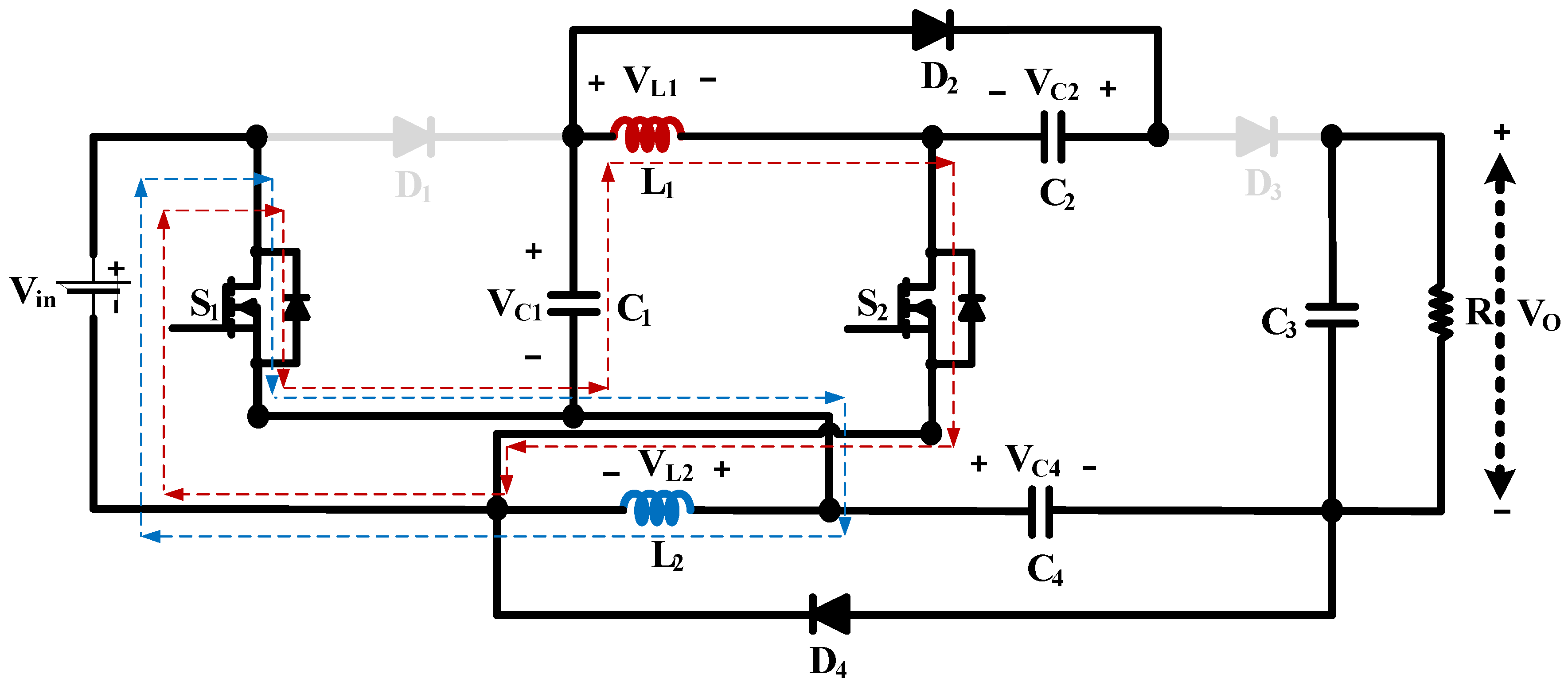
The proposed converter has two switches, and the same switching signal controls both. That is, both the switches are turned ON and turned OFF simultaneously. During the first mode of operation, when the control signal is high, both the switches are turned ON, diode D2 and D4 are conducting as shown in Figure 2.
The KVL equations during the first mode of operation are as follows:
V L 1 = V i n + V C 1 = V C 2
V L 2 = V i n = V C 4
During the first mode of operation, the current in both the inductor increases, capacitor C2 and C4 charged while C1 and C2 discharged, as shown in Figure 3.
During the second mode of operation, when both the switches are turned OFF, diode D1 and D3 are conducting while reaming two diodes are reversed biased as shown in Figure 4. The current in both the inductor decreases, capacitor C1 and C3 are charged while the other two capacitors are discharged. The related equations during this mode of operation are as follows:
V L 1 = 2 V i n + 2 V C 1 V O
V L 2 = V i n V C 1
Now applying volt-sec balance in inductor L2.
0 T V L 2 ( t ) · d t = 0
V i n × D T + ( V i n V C 1 ) × ( 1 D ) T = 0
V C 1 = V i n 1 D
Now applying volt-sec balance in inductor L1.
0 T V L 1 ( t ) · d t = 0
( V i n + V C 1 ) × D T + ( 2 V i n + 2 V C 1 V O ) × ( 1 D ) T = 0
After combining Equations (7) and (9), the voltage gain (M) of the converter can be written as:
V O = V i n ( 4 4 D + D 2 ) ( 1 D ) 2

Effect of Inductor’s Parasitic Resistance on Voltage Gain

Due to the circuit’s various components’ internal resistance, there are some power losses in the circuit. Because of these power losses, the voltage gain is not the same as explained before; it is reduced to some lower value. The output voltage, considering the power loss in the inductors, could be calculated as follows:
P i n = P o + P L l o s s t o t a l
P i n = V i n V O ( 4 4 D + D 2 ) R ( 1 D ) 2
P L l o s s t o t a l = ( V O R ( 1 D ) ) 2 r L 1 + ( V O ( 2 D ) R ( 1 D ) 2 ) 2 r l 2
P o = V O 2 R
After combining the above equations, the output voltage obtained as:
V O = V i n R ( 1 D ) 2 ( 4 4 D + D 2 ) R ( 1 D ) 4 + r L 1 ( 1 D ) 2 + r l 2 ( 2 D ) 2
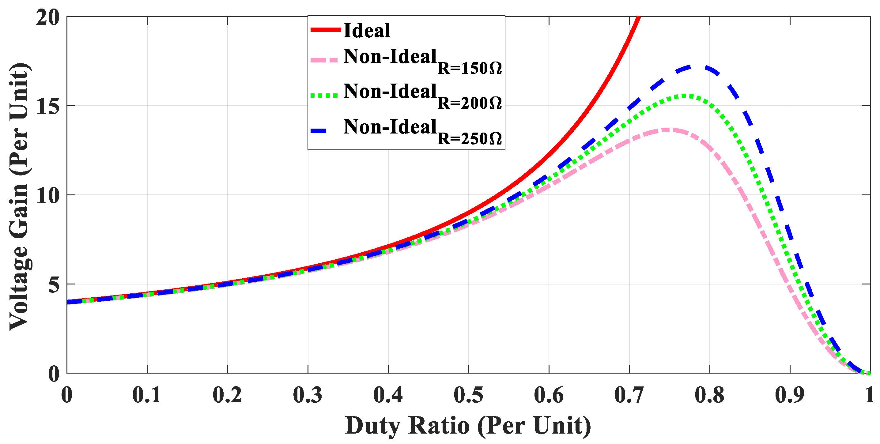
Using Equation (15), the proposed converter’s non-ideal voltage gain is calculated with the inductor’s parasitic resistance, which is 0.3 Ω for each inductor. The results are compared with the ideal conditions and presented in Figure 5. At lower duty ratios, both the ideal and real voltage gains are the same, but as the duty ratio increases, the deviation between these two becomes large. Further, the deviation increases with the decrease in the load resistance because a reduction in the load resistance increases the current in the circuit, which increases the power loss in the circuit. As the duty ratio is increased, the current in the circuit also increases, which increases conduction power loss in the circuit. Due to this reason, the efficiency of the DC-DC converters decreases at higher duty ratios, and the output voltage gain starts decreasing after reaching its maximum value. It is always recommended to use these converters below a certain value of a duty ratio.

3. Voltage Stress, Current and Passive Component Selection

The voltage stress across S1, S2, D2, and D4 is obtained by applying KVL during the second mode of operation, as shown in Figure 4. The voltage stress across diodes D1 and D3 could be obtained by applying KVL during the first mode of operation. The voltage stress and current across the switches and the diodes are shown in Table 1. It can be inferred from Table 1 that the voltage stress across switches and diodes is much less than the output voltage, which makes the converter highly efficient. The low voltage stress across capacitors, switches, and diodes and the high voltage gain at lower duty ratios is the distinguishing feature of the proposed converter, making it superior to the literature’s proposed topologies.
For the continuous mode of operation, the minimum current of each inductor should be greater than zero. The minimum current of the inductor depends on the current ripple and average current. The average current of each inductor and the minimum value of inductance of each inductor could be calculated as follows:
I L 1 = V O R ( 1 D )
I L 2 = V O ( 2 D ) R ( 1 D ) 2
L 1 R ( 1 D ) 2 ( 2 D ) D 2 f s ( 4 4 D + D 2 )
L 2 R ( 1 D ) 4 D 2 f s ( 4 4 D + D 2 ) ( 2 D )
The selection of the capacitors is based on the switching frequency as well as the permissible ripple in the voltage across the relationship between the capacitance, and other parameters are as follows:
C 1 = V O R ( 1 D ) f s Δ V C 1 = V i n ( 4 4 D + D 2 ) R ( 1 D ) 3 f s Δ V C 1
C 2 = V O R D f s Δ V C 2 = V i n ( 4 4 D + D 2 ) R D ( 1 D ) 2 f s Δ V C 2
C 3 = V O D R f s Δ V C 3 = V i n D ( 4 4 D + D 2 ) R ( 1 D ) 2 f s Δ V C 3
C 4 = V O R f s Δ V C 4 = V i n ( 4 4 D + D 2 ) R ( 1 D ) 2 f s Δ V C 4

4. Comparison with Other Recent Topologies

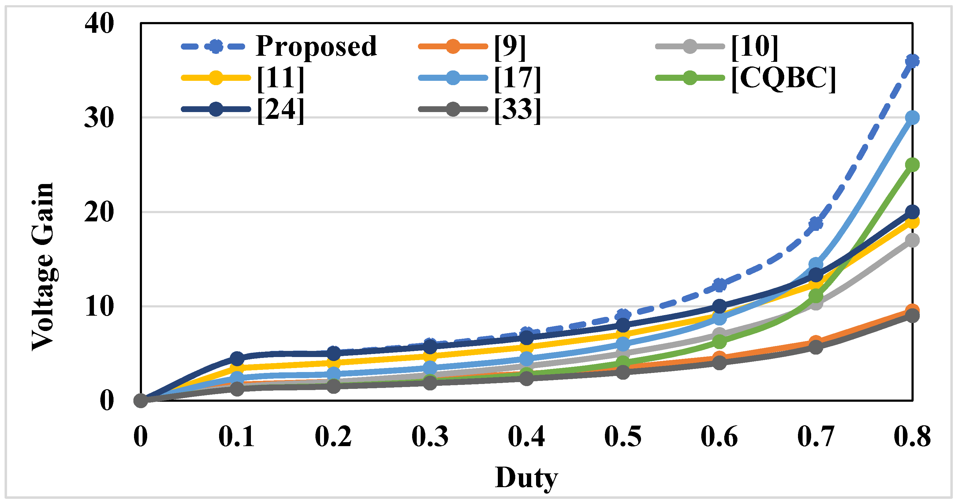
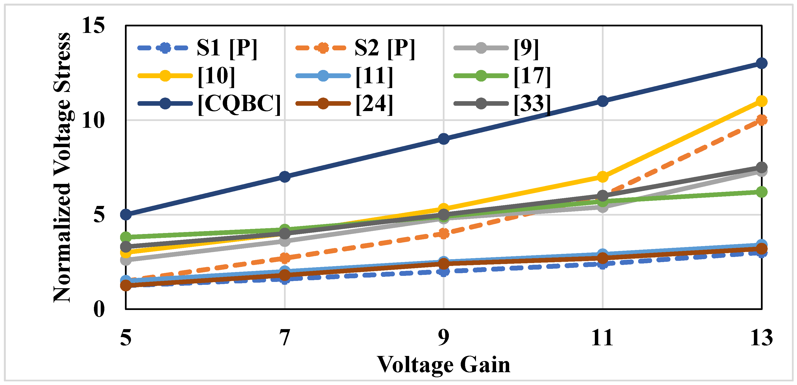
This section compares the proposed topology with some other recent structures of step-up converters. The proposed topology is compared with topologies with quadratic gain and ultra-high gain boost converter [24]. Table 2 shows the overall comparison of the proposed topology with other recent topologies, where N denotes the number of components. As depicted in Figure 6, the proposed topology has the highest gain in the entire operation range in the non-isolated category of converters with 12 components. The topology’s gain in [9] is less than the proposed converter, although it utilizes four inductors and a total of 14 components. The ultra-high gain boost converter is proposed in [24] and employs 12 components, but its gain is less than the proposed topology. The normalized voltage stress curve versus voltage gain is shown in Figure 7. The switch S1 has the lowest stress across all compared to the stress on all other topologies. The voltage stress across S2 is greater than S1, but for the voltage gain up to 10 times, it is lower than the stress of the converters in [9,10], [CQBC], and [33].

5. Simulation Results and Experimental Verification of the Proposed Converter

5.1. Simulation Results

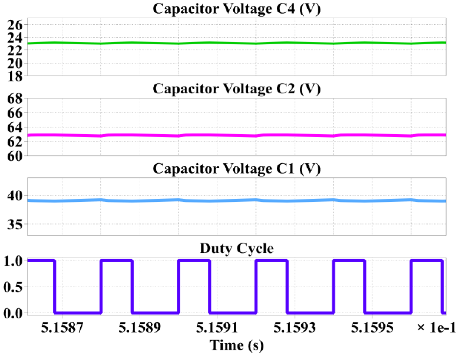
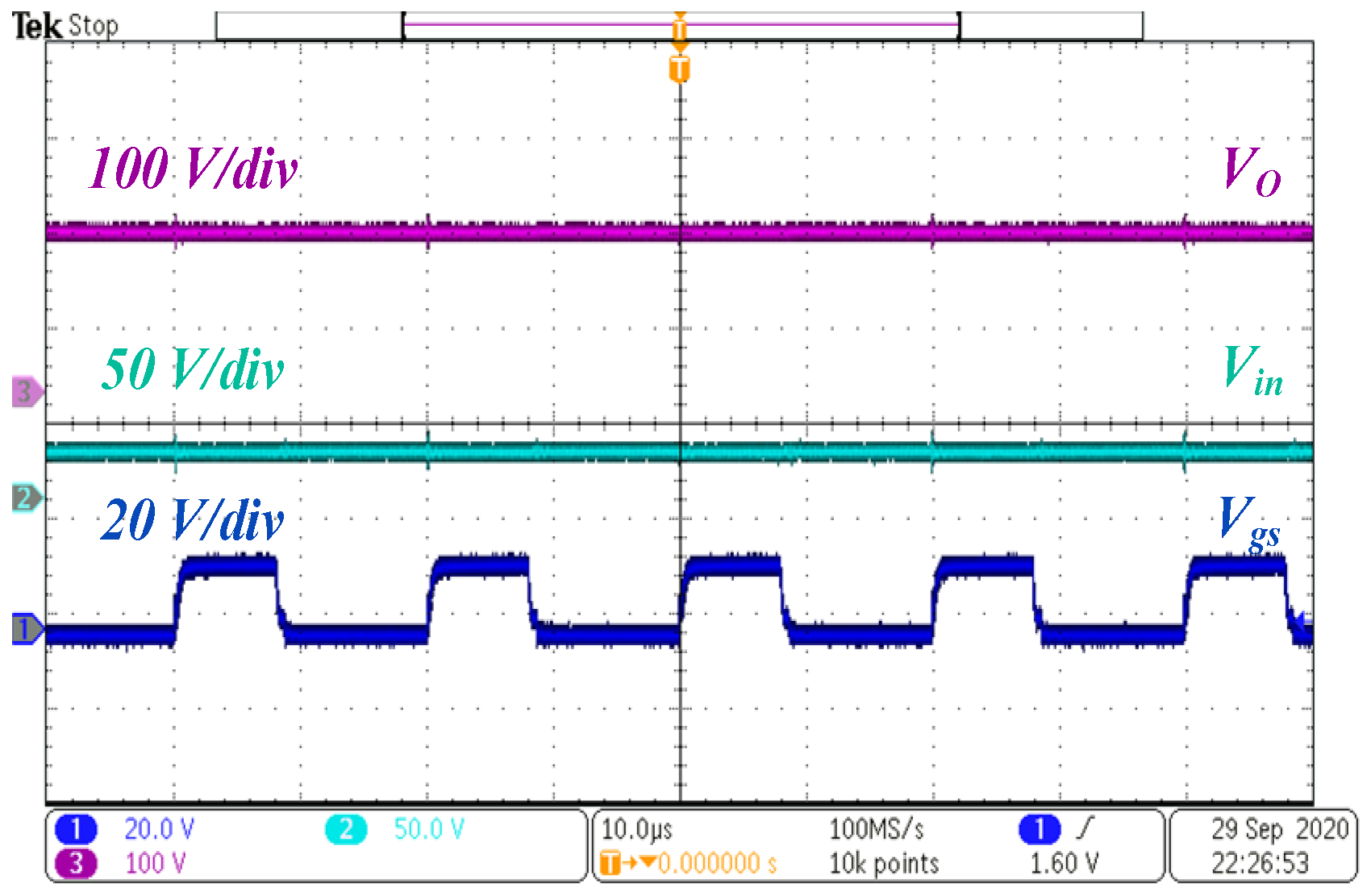
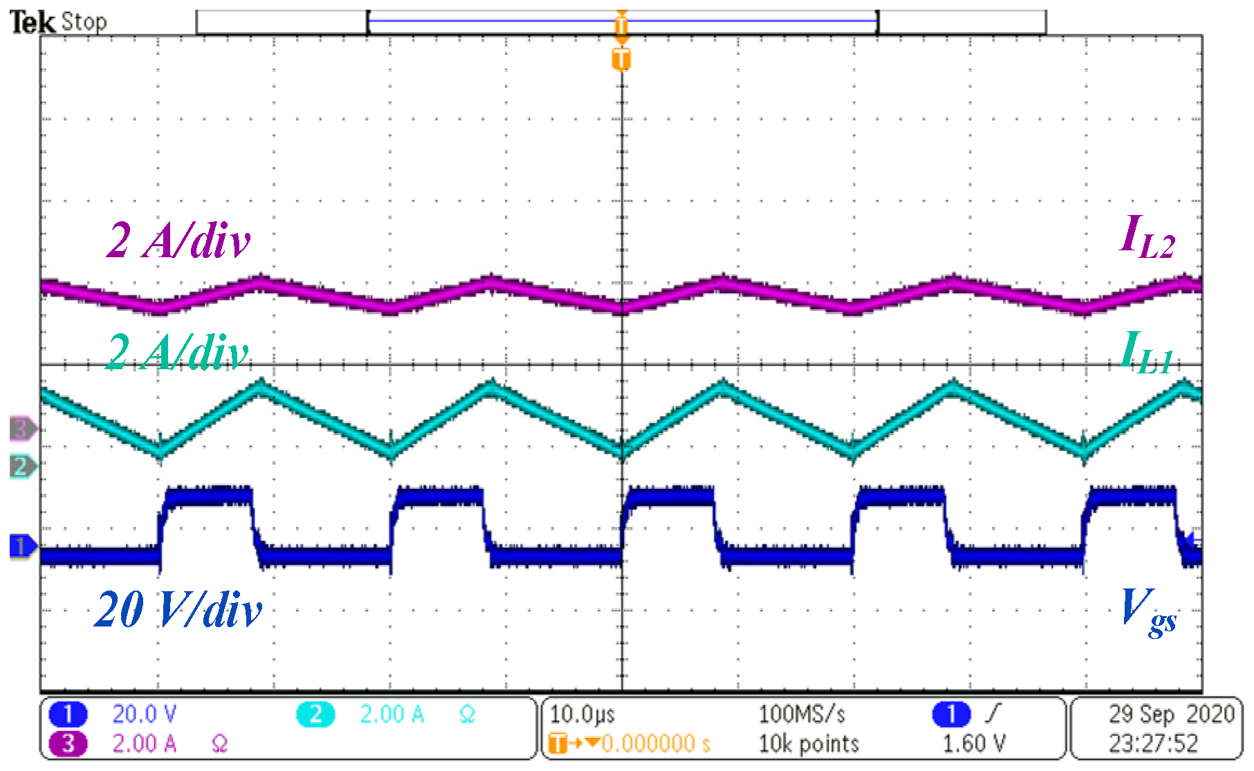
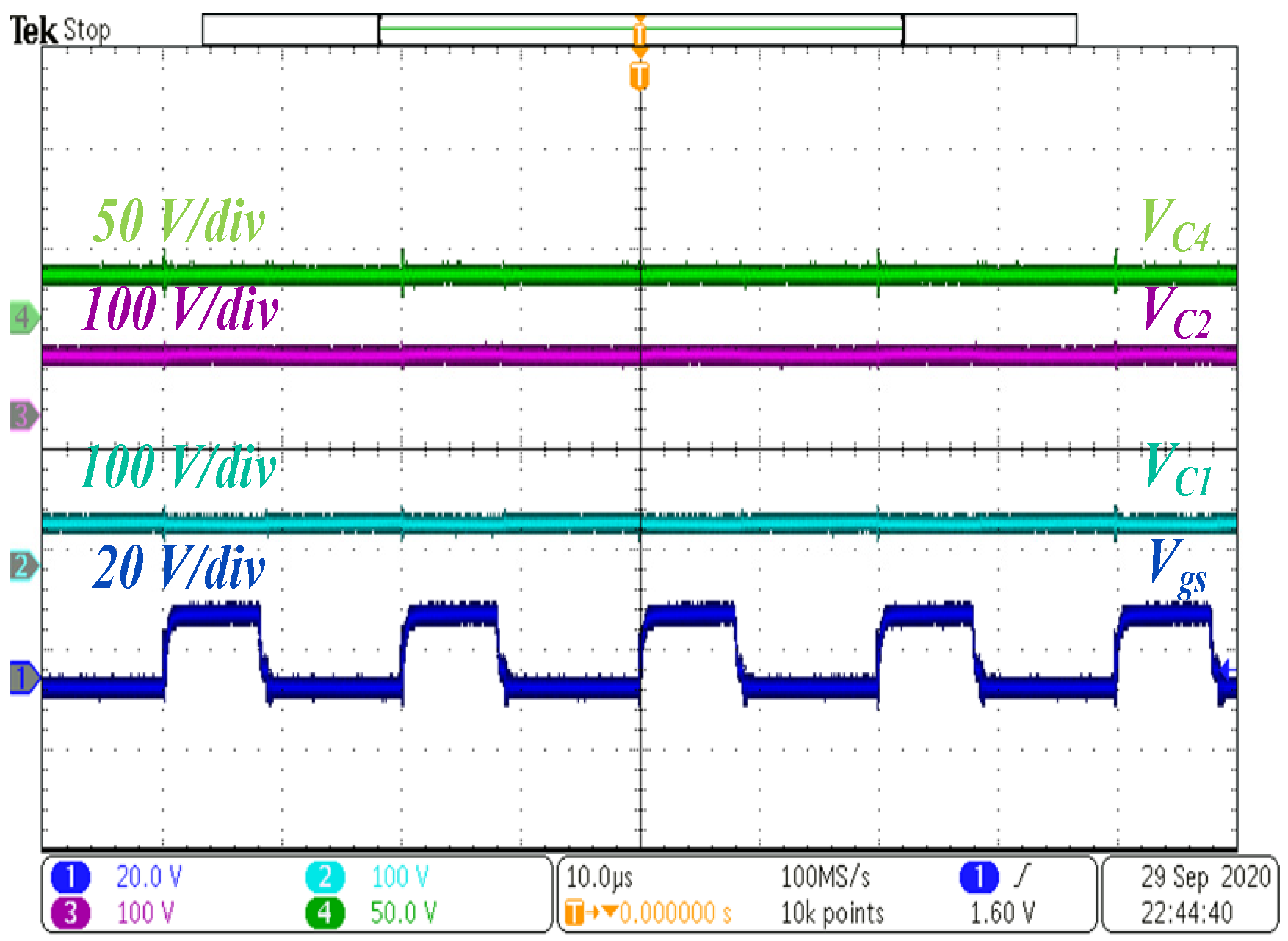
To test the effectiveness of the proposed converter, the simulations are performed using PLECS software. The Vo at Vin of 24 V and D = 0.4 is found to be 167 V, as shown in Figure 8. The small voltage drop is because of the parasitic and ON state resistances of the converter. The inductor current is continuous, and the average value of IL1 and IL2 is found to be 1.1 A and 3.3 A, respectively, as shown in Figure 9. The capacitor voltages are shown in Figure 10. The capacitor voltages of C1. C2 and C4 are 39 V, 63 V, and 23 V, respectively, which is an agreement with the theoretical analysis. The voltage stress across the capacitor is much less than the Vo, which leads to the selection of capacitors of low voltage rating. The choice of low rating components increases the efficiency of the converter. The stress across switch S1 and S2 is 40 V and 66 V, as depicted in Figure 11.

5.2. Experimental Verification

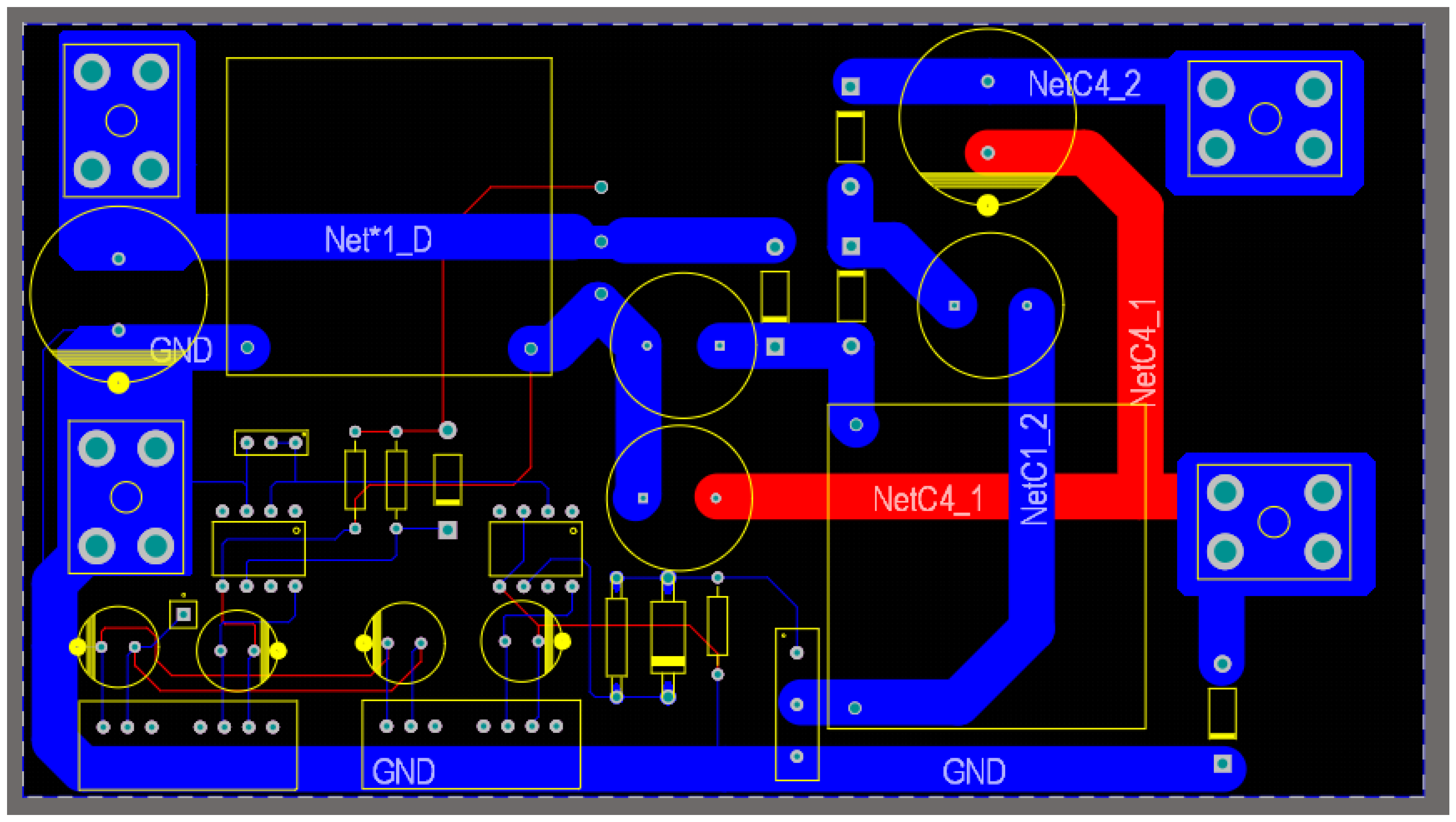
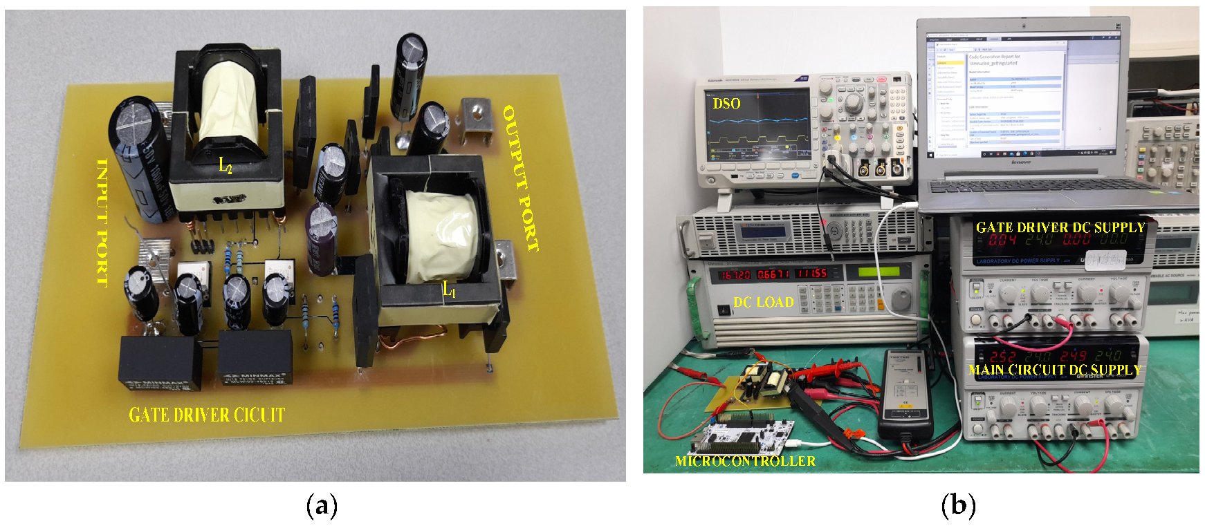
The hardware prototype is developed on the power circuit board (PCB) by using Altium Designer software. The designed PCB layout is shown in Figure 12. The hardware prototype is shown in Figure 13a, and the experimental setup is shown in Figure 13b. The specifications of the developed hardware prototype are shown in Table 3. The theoretical and simulation results are confirmed by developing a prototype and of 150 W in the lab. Figure 14 shows the experimental waveform of the Vo at Vin = 24 V and D = 0.4. Vo is found to be 167 V, which in agreement with the derived voltage gain. The high gain of 7 times is obtained at a low-duty ratio is the converter’s main advantage. The experimental inductor current waveforms are shown in Figure 15. The capacitor voltages are shown in Figure 16. The capacitor voltages of C1, C2, and C4 are much less than the output voltage Vo, which means that except for the output capacitor C3 all the other capacitors have low voltage stress across them.
The stress across switch S1 and S2, as depicted in Figure 17, is found to be 40 V and 66 V, which is also much less than the VO.

6. Efficiency Calculation

For the calculation of efficiency, the power loss in each component needs to be determined. The losses in switches are bifurcated into switching and conduction losses. The parasitic and ON state resistances are shown in Table 2. The total switching loss in switches S1 and S2 is found to be 0.298 W. The total conduction loss is found to be 0.773 W. The loss in capacitors:
{ P S l o s s c o n d u c t i o n = P S 1 l o s s c o n d u c t i o n + P S 2 l o s s c o n d u c t i o n P S l o s s c o n d u c t i o n = i S 1 R M S 2 × r S 1 + i S 2 R M S 2 × r S 2 = ( V O ( 2 D ) D R ( 1 D ) 2 ) 2 r S 1 + ( V O D R ( 1 D ) ) 2 r S 2 P S l o s s c o n d u c t i o n = 0.285   W P S l o s s s w i t c h i n g = ( t o n + t o f f ) ( I S 1 o n V S 1 o f f + I S 2 o n V S 2 o f f ) × f s 2 = 0.298   W P S l o s s ( c o n d u c t i o n + s w i t c h i n g ) = 0.583   W
The diode cut-in voltage for all diodes is 0.6 V the resistance is 0.06 Ω. The power loss for each of the diodes for an output voltage of 167 V and output power of 111.56 W can be calculated as shown.
{ P D 1 l o s s = V D 1 I D 1 a v g + i 2   D 1 R M S r D 1 P D 1 l o s s = 1.386   W P D 2 l o s s = V D 2 I D 2 a v g + i 2 D 2 R M S r D 2 P D 2 l o s s = 0.57 W P D 3 l o s s = V D 3 I D 3 a v g + i 2 D 3 R M S r D 3 P D 3 l o s s = 0.475   W P D 4 l o s s = V D 4 I D 4 a v g + i 2 D 4 R M S r D 4 P D 4 l o s s = 0.57   W P D l o s s t o t a l = 3.001   W
The total conduction losses in diodes are found to be 3 W.
The total conduction losses in capacitors are found to be 2.04 W.
{ P C l o s s t o t a l = i 2 C 1 R M S r C 1 + i 2 C 2 R M S r C 2 + i 2 C 3 R M S r C 3 + i 2 C 4 R M S r C 4 = ( V O R ( 1 D ) 1 + D D 2 D ) 2 r C 1 + ( V O R 1 D ( 1 D ) ) 2 r C 2 + ( V O R D ( 1 D ) ) 2 r C 3 + ( V O R 1 D ( 1 D ) ) 2 = 0.9   W + 0.55   W + 0.22   W + 0.37   W P C l o s s t o t a l = 2.04   W
The parasitic resistance of each coil is found to be 0.3 Ω. The loss in coils L1 and L2 can be computed as:
{ P L l o s s t o t a l = i 2 L 1 R M S r L 1 + i 2 L 2 R M S r L 2 = ( V O R ( 1 D ) ) 2 r L 1 + ( V O ( 2 D ) R ( 1 D ) 2 ) 2 r l 2 = 0.372   W + 2.64   W = 3.01   W
The total conduction losses in inductors are found to be 3.01 W. The bifurcation of losses in various components are shown in Figure 18. The loss in diodes and switches constitute around 46 percent of the total losses. The total loss in the converters is found to be 8.634 W.
Efficiency (η) of the converter can be expressed as:
{ η = P 0 P 0 + P , l o s s + P D , l o s s + P C , l o s s + P L ,   l o s s η % = 167 2 250 167 2 250 + 8.634 × 100 = 92.82 %
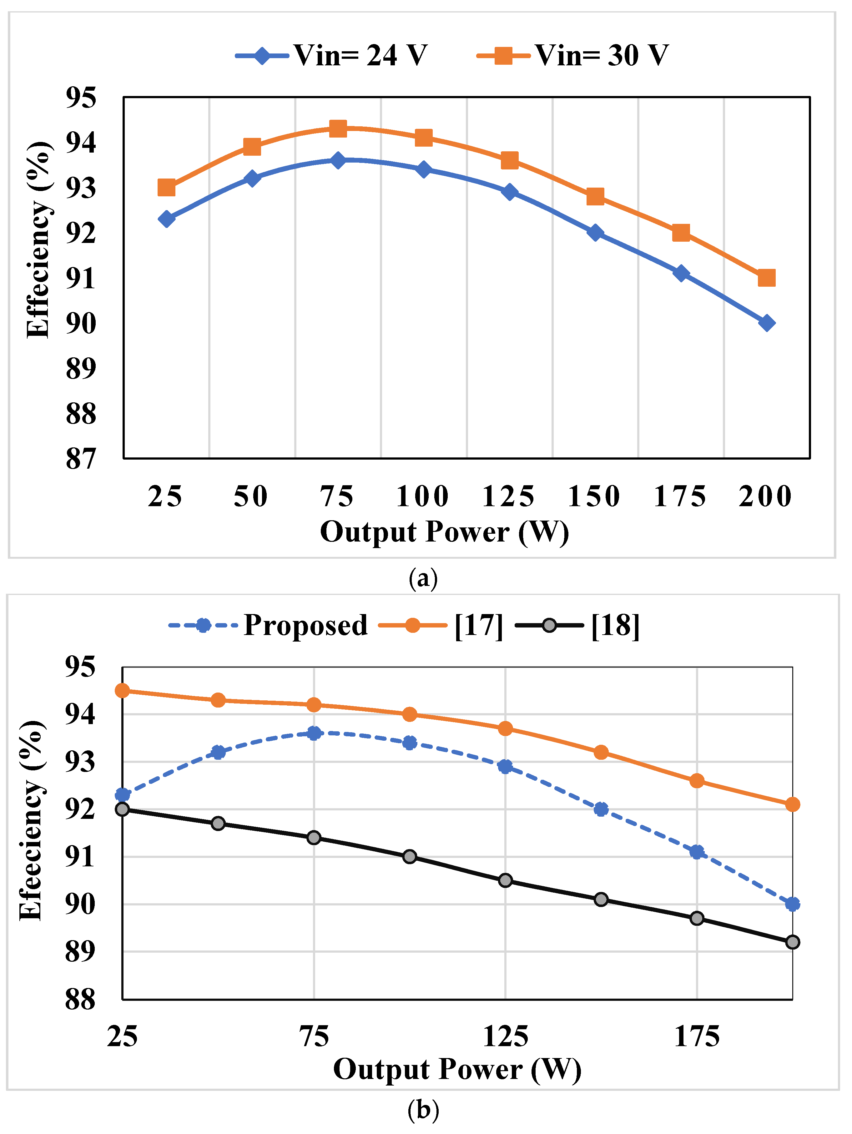
For an output power of 111.56 W, the efficiency is found to be 92.82%. The variation of efficiency with output power is shown in Figure 19a. The efficiency of the converter increases as the input voltage is increased. This increase in efficiency is because at higher input voltages, a small duty ratio is required to get the same amount of voltage gain, and hence conduction losses are significantly reduced. In Figure 19b, the comparison of efficiency at an input voltage of 24 V is shown. The coupled inductor topology proposed in [17] has higher efficiency than the proposed converter.

7. Performance of the Proposed Converter in Dynamic Conditions

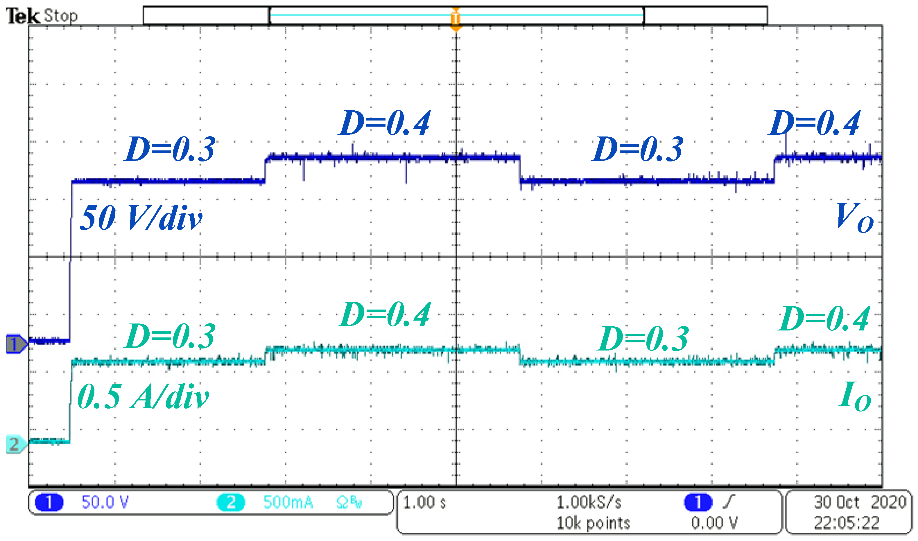
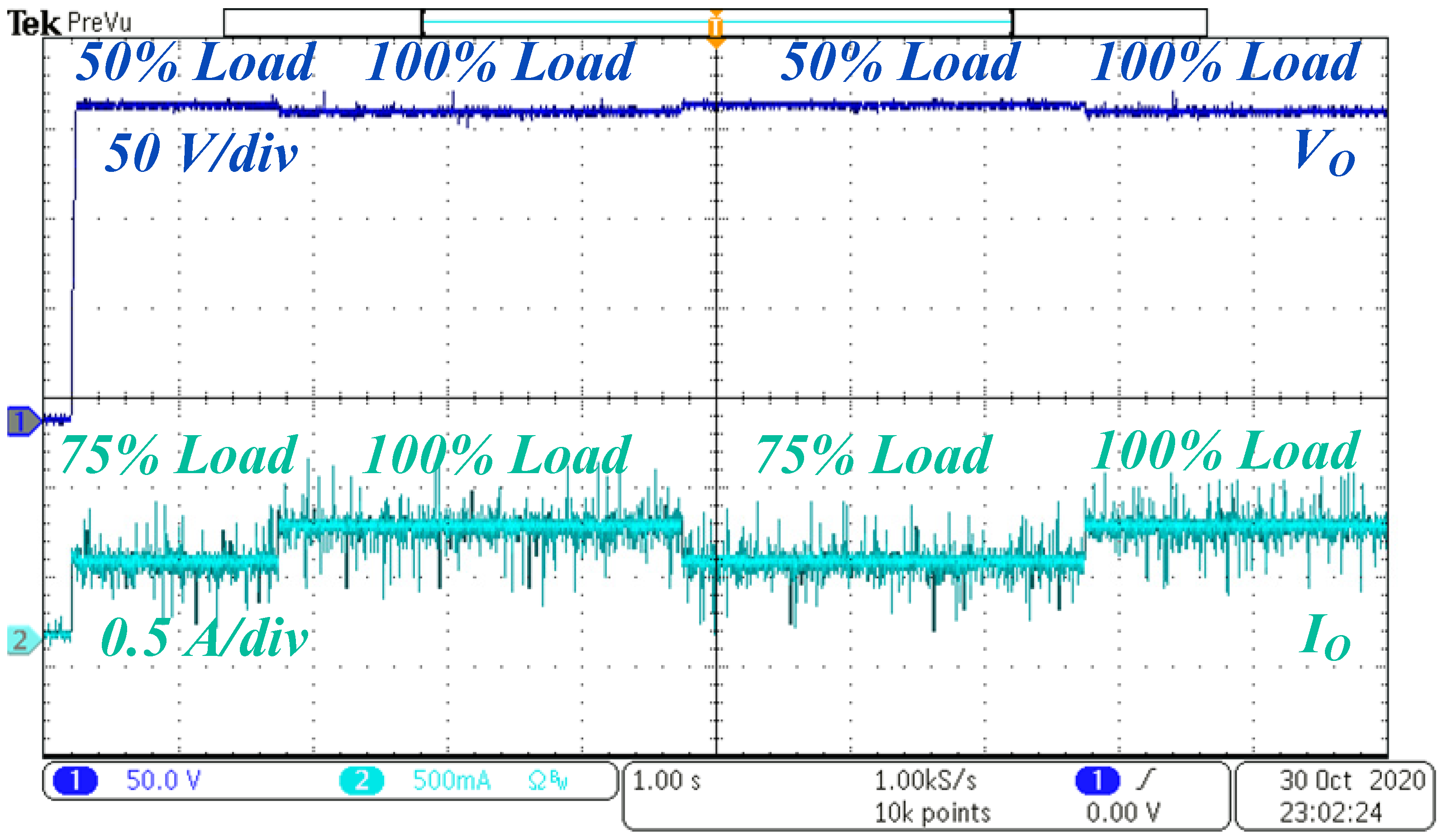
The dynamic conditions are presented in Figure 20 and Figure 21. While changing the duty ratio, the load resistance is kept constant at 200 Ω. With the increase in the duty ratio, the voltage gain increases without any transient, as shown in Figure 20. To capture the dynamic load change, the electronic load is set to change its load between 100% and 75% of the rated load, and the duty ratio is kept constant at 0.4. With the increase in the load, the output current increases, which increases the internal power losses in the circuit, and output voltage decreases a little bit, as shown in Figure 21.

8. Discussion

From the steady-state and dynamic performance, it can be observed that the converter is working satisfactorily in an open loop. The output voltage and currents obtained through experimental investigations closely match the theoretical and simulation results. Further, the stress across switches capacitors and diodes is less than the output voltage. The low voltage stress leads to the selection of devices with low voltage ratings, which ultimately improves efficiency and decreases the converter’s cost. The proposed converter is suitable for low and medium power applications. It is to be noted that the parasitic resistances of inductors decrease the voltage gain and the efficiency of the converter [38,39]. To increase the converter’s gain and efficiency at high duty ratios, a coupled inductor can also be used in the proposed topology instead of two separate inductors.

9. Conclusions

The main challenge in developing high gain DC-DC converters is to get high voltage gain by keeping the stress across devices low. Further, the number of components should also be optimized so that the converter cost is low and high efficiency can be obtained. These features are obtained in the proposed high gain converter. The converter has been successfully developed, and its performance is validated through simulation and experimental results. The converter’s loss analysis reveals its good performance with more than 91% efficiency throughout the input power range. The peak efficiency was found to be 93.6% at 66 W output power. The voltage gain of the converter is high at low duty ratios. A gain of more than 12 times can be achieved in ideal conditions at a duty ratio of 0.6. However, the actual gain depends on the parasitic values of different components and the load resistance. Overall, the proposed converter has shown good performance in non-isolated category of converters and can be employed in industrial, energy storage, and PV applications.

Author Contributions

Data curation, M.Z. (Mohammad Zaid) and M.F.; formal analysis, J.A., M.Z. (Mohammad Zaid) and A.S.; funding acquisition, S.A., M.S. and M.Z. (Mazen Zaindin); investigation, J.A., M.Z. (Mohammad Zaid) and A.S.; methodology, J.A., M.Z. (Mohammad Zaid), A.S., S.A., M.S. and M.F.; project administration, C.-H.L., S.A., M.S. and M.Z. (Mazen Zaindin); resources, C.-H.L., M.S. and M.Z. (Mazen Zaindin); software, C.-H.L., M.S., M.Z. (Mazen Zaindin), and M.F.; supervision, C.-H.L., A.S., M.Z. (Mohammad Zaid) and S.A.; validation, J.A., C.-H.L., M.Z. (Mohammad Zaid), A.S., and M.F; visualization, A.S., M.Z. (Mohammad Zaid), M.Z. (Mazen Zaindin) and M.F; writing—original draft preparation, J.A. and M.Z. (Mohammad Zaid); writing—review and editing, A.S., J.A., M.Z. (Mohammad Zaid) and S.A. All authors have read and agreed to the published version of the manuscript.

Funding

This research received funding from Deputyship for Research & Innovation, “Ministry of Education” in Saudi Arabia through the project number IFKSURG-1438-089.

Acknowledgments

The authors extend their appreciation to the Deputyship for Research & Innovation, “Ministry of Education” in Saudi Arabia for funding this research work through the project number IFKSURG-1438-089.

Conflicts of Interest

The authors declare no conflict of interest.

Abbreviation

V i n Input Voltage
V O Output Voltage
V L Inductor Voltage
V C Capacitor Voltage
Δ V C Capacitor Voltage Ripple
Δ I L Inductor Current Ripple
RLoad Resistance
DDuty Ratio
P i n Input Power
P O Output Power
P l o s s Power Loss
rL1,rL2Parasitic resistance of inductor
rC1,rC2,rC3,rC4Parasitic resistance of capacitors
rD1,rD2,rD3,rD4Parasitic resistance of diodes

References

  1. Almalaq, Y.; Matin, M. Three Topologies of a Nonisolated High Gain Switched-Inductor Switched-Capacitor Step-Up Cuk Converter for Renewable Energy Applications. Electronics 2018, 7, 94. [Google Scholar] [CrossRef] [Green Version]
  2. Padmanaban, S.; Bhaskar, M.S.; Maroti, P.K.; Blaabjerg, F.; Fedák, V. An Original Transformer and Switched-Capacitor (T & SC)-Based Extension for DC-DC Boost Converter for High-Voltage/Low-Current Renewable Energy Applications: Hardware Implementation of a New T & SC Boost Converter. Energies 2018, 11, 783. [Google Scholar] [CrossRef] [Green Version]
  3. Bhaskar, M.S.; Ramachandaramurthy, V.K.; Padmanaban, S.; Blaabjerg, F.; Ionel, D.M.; Mitolo, M.; Almakhles, D. Survey of DC-DC Non-Isolated Topologies for Unidirectional Power Flow in Fuel Cell Vehicles. IEEE Access 2020, 8, 178130–178166. [Google Scholar] [CrossRef]
  4. Forouzesh, M.; Siwakoti, Y.P.; Gorji, S.A.; Blaabjerg, F.; Lehman, B. Step-Up DC–DC Converters: A Comprehensive Review of Voltage-Boosting Techniques, Topologies, and Applications. IEEE Trans. Power Electron. 2017, 32, 9143–9178. [Google Scholar] [CrossRef]
  5. Tofoli, F.L.; De Pereira, D.C.; Josias de Paula, W.; de Oliveira Júnior, D.S. Survey on nonisolated high-voltage step-up dc–dc topologies based on the boost converter. IET Power Electron. 2015, 8, 2044–2057. [Google Scholar] [CrossRef] [Green Version]
  6. Rosas-Caro, J.C.; Ramirez, J.M.; Peng, F.Z.; Valderrabano, A. A DC-DC multilevel boost converter. IET Power Electron. 2010, 3, 129–137. [Google Scholar] [CrossRef]
  7. Sarikhani, A.; Allahverdinejad, B.; Hamzeh, M. A Non-Isolated Buck-Boost DC-DC Converter with Continuous Input Current for Photovoltaic Applications. IEEE J. Emerg. Sel. Top. Power Electron. 2020. [Google Scholar] [CrossRef]
  8. Shahir, F.M.; Babaei, E.; Farsadi, M. Extended Topology for a Boost DC–D.C. Converter. IEEE Trans. Power Electron. 2019, 34, 2375–2384. [Google Scholar] [CrossRef]
  9. Saravanan, S.; Babu, N.R. Design and Development of Single Switch High Step-Up DC–D.C. Converter. IEEE J. Emerg. Sel. Top. Power Electron. 2018, 6, 855–863. [Google Scholar] [CrossRef]
  10. Tang, Y.; Fu, D.; Wang, T.; Xu, Z. Hybrid Switched-Inductor Converters for High Step-Up Conversion. IEEE Trans. Ind. Electron. 2015, 62, 1480–1490. [Google Scholar] [CrossRef]
  11. Tang, Y.; Wang, T.; He, Y. A Switched-Capacitor-Based Active-Network Converter With High Voltage Gain. IEEE Trans. Power Electron. 2014, 29, 2959–2968. [Google Scholar] [CrossRef]
  12. Arunkumari, T.; Indragandhi, V.; Arunkumar, G.; Sanjeevikumar, P.; Holm-Nielsen, J.B. Implementation of high-gain nonisolated DC-DC converter for PV-fed applications. Int. Trans. Electr. Energy Syst. 2020, 30, e12165. [Google Scholar] [CrossRef]
  13. Wu, G.; Ruan, X.; Ye, Z. Nonisolated High Step-Up DC–D.C. Converters Adopting Switched-Capacitor Cell. IEEE Trans. Ind. Electron. 2015, 62, 383–393. [Google Scholar] [CrossRef]
  14. Miao, S.; Wang, F.; Ma, X. A New Transformerless Buck–Boost Converter With Positive Output Voltage. IEEE Trans. Ind. Electron. 2016, 63, 2965–2975. [Google Scholar] [CrossRef]
  15. Saadat, P.; Abbaszadeh, K. A Single-Switch High Step-Up DC–D.C. Converter Based on Quadratic Boost. IEEE Trans. Ind. Electron. 2016, 63, 7733–7742. [Google Scholar] [CrossRef]
  16. Moradpour, R.; Tavakoli, A. A DC–D.C. boost converter with high voltage gain integrating three-winding coupled inductor with low input current ripple. Int. Trans. Electr. Energy Syst. 2020, 30, e12383. [Google Scholar] [CrossRef]
  17. Lee, S.-W.; Do, H.-L. Quadratic Boost DC–D.C. Converter With High Voltage Gain and Reduced Voltage Stresses. IEEE Trans. Power Electron. 2019, 34, 2397–2404. [Google Scholar] [CrossRef]
  18. Wang, Y.; Qiu, Y.; Bian, Q.; Guan, Y.; Xu, D. A Single Switch Quadratic Boost High Step Up DC–D.C. Converter. IEEE Trans. Ind. Electron. 2019, 66, 4387–4397. [Google Scholar] [CrossRef]
  19. Bhaskar, M.S.; Almakhles, D.J.; Padmanaban, S.; Holm-Nielsen, J.B.; Kumar, A.R.; Masebinu, S.O. Triple-Mode Active-Passive Parallel Intermediate Links Converter With High Voltage Gain and Flexibility in Selection of Duty Cycles. IEEE Access 2020, 8, 134716–134727. [Google Scholar] [CrossRef]
  20. Abdel-Rahim, O.; Funato, H.; Haruna, J. A comprehensive study of three high-gain DC-DC topologies based on Cockcroft-Walton voltage multiplier for reduced power P.V. applications. IEEJ Trans. Electr. Electron. Eng. 2018, 13, 642–651. [Google Scholar] [CrossRef]
  21. Mohammadzadeh Shahir, F.; Babaei, E. A new structure for nonisolated boost dc-dc converter based on voltage-lift technique. In Proceedings of the 2017 8th Power Electronics, Drive Systems Technologies Conference (PEDSTC), Mashhad, Iran, 14–16 February 2017; pp. 25–30. [Google Scholar]
  22. Alzahrani, A.; Ferdowsi, M.; Shamsi, P. A Family of Scalable Non-Isolated Interleaved DC-DC Boost Converters With Voltage Multiplier Cells. IEEE Access 2019, 7, 11707–11721. [Google Scholar] [CrossRef]
  23. Meraj, M.; Bhaskar, M.S.; Iqbal, A.; Al-Emadi, N.; Rahman, S. Interleaved Multilevel Boost Converter With Minimal Voltage Multiplier Components for High-Voltage Step-Up Applications. IEEE Trans. Power Electron. 2020, 35, 12816–12833. [Google Scholar] [CrossRef]
  24. Pan, C.-T.; Chuang, C.-F.; Chu, C.-C. A Novel Transformer-less Adaptable Voltage Quadrupler DC Converter with Low Switch Voltage Stress. IEEE Trans. Power Electron. 2014, 29, 4787–4796. [Google Scholar] [CrossRef]
  25. Padmavathi, P.; Natarajan, S. Single switch quasi Z-source based high voltage gain DC-DC converter. Int. Trans. Electr. Energy Syst. 2020, 30, e12399. [Google Scholar] [CrossRef]
  26. Abbasi Aghdam Meinagh, F.; Yuan, J.; Yang, Y. Analysis and design of a high voltage-gain quasi-Z-source D.C.–D.C. converter. IET Power Electron. 2020, 13, 1837–1847. [Google Scholar] [CrossRef]
  27. Martinez, W.; Cortes, C.; Yamamoto, M.; Imaoka, J. Effect of inductor parasitic resistances on the voltage gain of high step-up D.C.–D.C. converters for electric vehicle applications. IET Power Electron. 2018, 11, 1628–1639. [Google Scholar] [CrossRef]
  28. Banaei, M.R.; Bonab, H.A.F. High-efficiency transformerless buck–boost D.C.–D.C. converter. Int. J. Circuit Theory Appl. 2017, 45, 1129–1150. [Google Scholar] [CrossRef]
  29. Lakshmi, M.; Hemamalini, S. Nonisolated High Gain DC–D.C. Converter for D.C. Microgrids. IEEE Trans. Ind. Electron. 2018, 65, 1205–1212. [Google Scholar] [CrossRef]
  30. Yang, P.; Xu, J.; Zhou, G.; Zhang, S. A new quadratic boost converter with high voltage step-up ratio and reduced voltage stress. In Proceedings of the 7th International Power Electronics and Motion Control Conference, Harbin, China, 2–5 June 2012; Volume 2, pp. 1164–1168. [Google Scholar]
  31. Jalilzadeh, T.; Rostami, N.; Babaei, E.; Maalandish, M. Nonisolated Topology for High Step-Up DC-DC Converters. IEEE J. Emerg. Sel. Top. Power Electron. 2018. [Google Scholar] [CrossRef]
  32. Hu, D.; Yin, A.; Ghaderi, D. A transformer-less single-switch boost converter with high-voltage gain and mitigated-voltage stress applicable for photovoltaic utilizations. Int. Trans. Electr. Energy Syst. 2020, 30, e12569. [Google Scholar] [CrossRef]
  33. Shahir, F.M.; Babaei, E.; Farsadi, M. Voltage-Lift Technique Based Nonisolated Boost DC–D.C. Converter: Analysis and Design. IEEE Trans. Power Electron. 2018, 33, 5917–5926. [Google Scholar] [CrossRef]
  34. Park, H.; Kim, S. Single Inductor Multiple Output Auto-Buck-Boost DC–D.C. Converter with Error-Driven Randomized Control. Electronics 2020, 9, 1335. [Google Scholar] [CrossRef]
  35. Shi, F.; Song, D. A Novel High-Efficiency Double-Input Bidirectional DC/DC Converter for Battery Cell-Voltage Equalizer with Flyback Transformer. Electronics 2019, 8, 1426. [Google Scholar] [CrossRef] [Green Version]
  36. Ahmad, A.; Anas, M.; Sarwar, A.; Zaid, M.; Tariq, M.; Ahmad, J.; Beig, A.R. Realization of a Generalized Switched-Capacitor Multilevel Inverter Topology with Less Switch Requirement. Energies 2020, 13, 1556. [Google Scholar] [CrossRef] [Green Version]
  37. Ahmad, J.; Zaid, M.; Sarwar, A.; Tariq, M.; Sarwer, Z. A New Transformerless Quadratic Boost Converter with High Voltage Gain. Smart Sci. 2020, 8, 163–183. [Google Scholar] [CrossRef]
  38. Bellar, M.D.; Watanabe, E.H.; Mesquita, A.C. Analysis of the dynamic and steady-state performance of Cockcroft-Walton cascade rectifiers. IEEE Trans. Power Electron. 1992, 7, 526–534. [Google Scholar] [CrossRef]
  39. Ballo, A.; Bottaro, M.; Grasso, A.D.; Palumbo, G. Regulated Charge Pumps: A Comparative Study by Means of Verilog-AMS. Electronics 2020, 9, 998. [Google Scholar] [CrossRef]
  40. Ballo, A.; Grasso, A.D.; Palumbo, G. A Review of Charge Pump Topologies for the Power Management of IoT Nodes. Electronics 2019, 8, 480. [Google Scholar] [CrossRef] [Green Version]
  41. Liu, M. Demystifying Switched Capacitor Circuits; Elsevier: Amsterdam, The Netherlands, 2006. [Google Scholar]
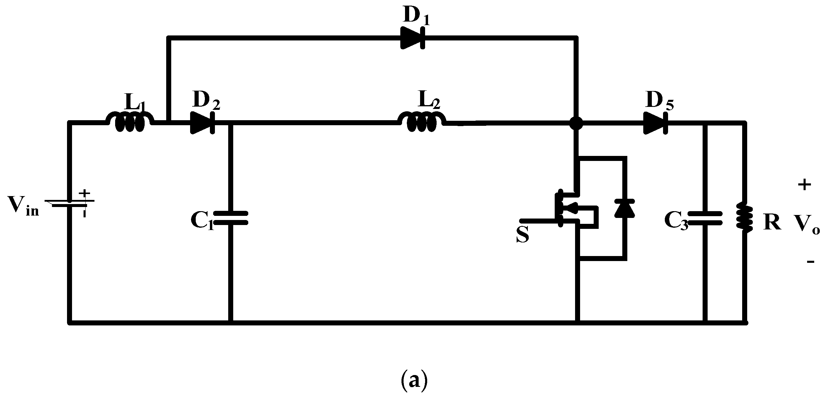
Figure 1. (a) Conventional quadratic boost converter (CQBC); (b). Proposed converter.
Electronics 09 02067 g001aElectronics 09 02067 g001b
Figure 2. First mode of operation.
Electronics 09 02067 g002
Figure 3. Related waveforms in continuous conduction mode (CCM).
Electronics 09 02067 g003
Figure 4. The second mode of operation.
Electronics 09 02067 g004
Figure 5. Ideal voltage gain and real voltage gain.
Electronics 09 02067 g005
Figure 6. Comparison of Voltage gain vs. Duty ratio of proposed converter with other converters.
Electronics 09 02067 g006
Figure 7. Normalized voltage stress vs. Voltage gain.
Electronics 09 02067 g007
Figure 8. Output Voltage at 24 V input and D = 0.4.
Electronics 09 02067 g008
Figure 9. Inductor currents of L1 and L2 at D = 0.4.
Electronics 09 02067 g009
Figure 10. Capacitor voltages of C1, C2, and C4 at D = 0.4.
Electronics 09 02067 g010
Figure 11. Output voltage and voltage stress across switch S1 and S2 at D = 0.4.
Electronics 09 02067 g011
Figure 12. Proposed Converter power circuit board (PCB) Layout.
Electronics 09 02067 g012
Figure 13. (a) Proposed converter; (b) experimental set-up.
Electronics 09 02067 g013
Figure 14. Output voltage at 24 V input and D = 0.4.
Electronics 09 02067 g014
Figure 15. Inductor currents of L1 and L2 at D = 0.4.
Electronics 09 02067 g015
Figure 16. Capacitor voltages of C1, C2, and C4 at D = 0.4.
Electronics 09 02067 g016
Figure 17. Output voltage and voltage stress across switch S1 and S2 at D = 0.4.
Electronics 09 02067 g017
Figure 18. Bifurcation of losses in the proposed converter.
Electronics 09 02067 g018
Figure 19. (a) Experimental efficiency of the converter; (b) Comparison of efficiency of the proposed converter.
Electronics 09 02067 g019
Figure 20. Effect of the change in duty on VO and IO.
Electronics 09 02067 g020
Figure 21. Effect of change in load on VO and IO.
Electronics 09 02067 g021
Table 1. Voltage stress and current across the switches and diodes.
ComponentVoltage Stress (Volt)Average Current during Their Conduction (Amp)Average Current for the Complete Cycle (Amp)RMS Current (Amp)
S1 V i n ( 1 D ) = V O ( 1 D ) ( 4 4 D + D 2 ) V O ( 2 D ) R ( 1 D ) 2 V O ( 2 D ) D R ( 1 D ) 2 V O ( 2 D ) D R ( 1 D ) 2
S2 V i n ( 1 D ) 2 = V O ( 4 4 D + D 2 ) V O R D ( 1 D ) V O D R D ( 1 D ) V O D R ( 1 D )
D1 V i n ( 1 D ) = V O ( 1 D ) ( 4 4 D + D 2 ) V O ( 2 D ) R ( 1 D ) 2 V O ( 2 D ) R ( 1 D ) V O ( 2 D ) R ( 1 D ) 3 / 2
D2 2 V i n ( 1 D ) = 2 V O ( 1 D ) ( 4 4 D + D 2 ) V O R D V O R V O R D
D3 V i n ( 2 D ) ( 1 D ) 2 = V O ( 2 D ) ( 4 4 D + D 2 ) V O R ( 1 D ) V O R V O R 1 D
D4 V i n ( 1 D ) = V O ( 1 D ) ( 4 4 D + D 2 ) V O R D V O R V O R D
Table 2. Comparison of the proposed topology with other similar topologies.
TopologyNL
(Inductors)
NC
(Capacitors)
NSW
(Switches)
ND
(Diodes)
M
( V o / V i n )
S
( V S / V i n )
[9]2414 3 + D 2 ( 1 D ) 1 1 D
[10]4127 1 + 3 D ( 1 D ) 1 + D 1 D
[11]2323 3 + D ( 1 D ) 1 1 D
[17]1+1 coupled inductor315 2 D ( 1 D ) 2 n = 1 2 1 D
[CQBC]2213 1 ( 1 D ) 2 1 ( 1 D ) 2
[24]2424 4 ( 1 D ) 1 1 D
[33]2313 1 + D 1 D 1 1 D
Proposed2424 4 4 D + D 2 ( 1 D ) 2 S 1 = 1 1 D
S 2 = 1 ( 1 D ) 2
Table 3. Specifications of the proposed converter.
ElementsSpecification
Input Voltage (Vin)24 V
Maximum Output Power150 W
Switching Frequency50 kHz
Load ResistanceR = 250 Ω, Electronic load simulator
InductorsL1 = L2 = 330 µH, ESR = 0.3 Ω
CapacitorsC1 = 47 µF/100 V ESR = 0.26 Ω, C2 = C3 = 33 µF/200 V ESR = 0.3 Ω & C4 = 220 µF/50 V ESR = 0.20 Ω
Power MOSFET (S1 & S2)SPW52N50C3, RDSon = 70 mΩ
Diodes (D1, D2, D3 & D4)SF8L60USM, Vd = 0.6 V
Gate Drivers ICTLP250H
Gate Driver Voltage Regulator ICMCWI03-48S15
MicrocontrollerSTM32 Nucleo H743ZI2
Publisher’s Note: MDPI stays neutral with regard to jurisdictional claims in published maps and institutional affiliations.