Article

Improvement of Multilevel DC/DC Converter for E-Mobility Charging Station

1
Department of Electrical Engineering, Chonnam National University, Buk-gu, Gwangju 61186, Korea
2
Department of Automotive Engineering, Honam University, Gwangsan-gu, Gwangju 62399, Korea
*
Author to whom correspondence should be addressed.
Electronics 2020, 9(12), 2037; https://doi.org/10.3390/electronics9122037
Submission received: 6 November 2020 / Revised: 24 November 2020 / Accepted: 27 November 2020 / Published: 1 December 2020
(This article belongs to the Section Power Electronics)

Abstract

:
Considerable efforts are being made to reduce CO2 emissions and thereby solve the problems of environmental pollution and global warming. Technologies for environmentally friendly transportation are being developed using batteries. In particular, with the increase in urbanization and one-person households, e-mobility products are drawing increasing attention as short-distance transportation devices. Among these vehicles, personal mobility devices (PMDs) are receiving attention as new transportation devices that are simple to operate. This paper proposes a new multilevel charging system that is advantageous in responding to the charging voltage specifications of various mobile devices with a single charging system while ensuring a low charging current ripple. The proposed diode-parallel multilevel converter consists of an independent Buck converter in series. The switch of the buck converter is configured at the negative terminal of the input power source so that the gate amplifier voltage is used as the power supply voltage; it can therefore be simply configured without a separate gate amplifier power supply. In addition, it is improved so as to have a wider charging voltage range in a low output voltage region and a better efficiency than the existing diode series multilevel converter. To verify the feasibility of the proposed system, simulations were performed using the software PowerSIM(PSIM), and, in order to verify the validity, a prototype charging system was fabricated to compare and analyze losses according to operating conditions.

1. Introduction

Currently, urbanization is increasing rapidly around the world. According to the World Urbanization Prospects, the number of megacities with a population of 10 million people or more is predicted to increase from 14 in 1995 to 46 in 2035 (Figure 1). Accordingly, an increasing number of people are moving from rural areas to cities, and the global share of the urban population is expected to increase from 45% in 1995 to 62% in 2035. This is because massive centralized cities where production, consumption, education, and cultural development can be realized in a single region are advantageous in terms of economic efficiency [1,2,3].
In many developed countries, urbanization has naturally developed as a measure to improve the return on investment and secure the services of talented people. However, because of the increase in the number of megacities and population density, several threats are affecting the quality of life of urban residents, and these threats are increasing rapidly. One of these threats is excessive energy consumption and environmental pollution due to the increase in the number of industrial complexes and high-rise buildings aimed at improving public convenience, and due to the resulting traffic overload on the transportation infrastructure resulting from the use of vehicles running on internal combustion engines. Many methods have been attempted to solve this problem. One of these methods is the paradigm shift from internal combustion engine vehicles using fossil fuels to electric vehicles (EVs) using environmentally friendly electrical energy. However, although the use of EVs can solve some environmental problems, it is still difficult to solve parking and traffic congestion problems by using EVs. In particular, because of the centralization of population and the operation of passenger vehicles with one or two passengers per vehicle, the number of vehicles in the city center is increasing sharply, resulting in parking and traffic congestion problems [4,5].
Accordingly, the development of various types of e-mobility devices that are environmentally friendly and capable of improving mobility is being accelerated in order to solve environmental and social problems simultaneously. E-mobility is a general term for the use of personal means of transportation for one or two persons using an ecofriendly electric drive method that is different from that used in existing passenger cars. E-mobility devices can be largely classified into micromobility devices, smart mobility devices, and personal mobility devices (PMDs). In addition, there are different types of e-mobility devices, such as upright-type devices, electric bicycles, and two- and three-wheeled vehicles.
Among e-mobility devices, PMDs are used in downtown areas, large-scale development areas, and residential areas for commuting, leisure, and business, and they are expected to make significant contributions to the development of solutions to traffic difficulties and the prevention of environmental pollution. Consequently, the PMD market is rapidly growing. Bird, an American startup company, has confirmed the marketability of PMDs through its electric kickboard sharing business, and automakers and large companies are actively promoting the PMD business [6,7].
However, a few challenges must be overcome for the successful introduction of PMDs. First, the definition of PMDs and their distinction from other vehicles are not clear, and from a legal perspective operational regulations need to be established and postaccident handling problems must be solved. Thus, the proper environment for using PMDs must be created through the establishment of systems and laws. In this regard, governments and institutions are striving to improve related laws and systems to promote the introduction of PMDs. Once PMDs have stably established their place in the market as short-distance transportation devices through the aforementioned improved environment, another critical challenge would be to build the charging infrastructure. Charging stations for EVs are widely distributed. However, e-mobility devices, including PMDs, use various voltages and currents for their batteries according to various device types, manufacturers, and equipment characteristics. Therefore, they are charged using exclusive external-adapter-type chargers. However, these chargers have an excessive volume and weight because their circuits must be configured to satisfy various safety regulations and certification standards for electrical appliances; hence, carrying them is inconvenient. Therefore, to facilitate the spread of PMDs, which can cover only short-to-medium distances, charging stations that can charge various types of PMDs need to be developed [8,9,10,11].
The requirements for charging stations for PMDs can be primarily divided into two categories. First, ultrasmall PMDs such as electric wheels and electric kickboards are designed for 250 W or lower and mainly use 12-, 24-, 36-, or 48-V power supplies, whereas PMDs such as electric motorcycles and ultrasmall EVs are designed for 750–1500 W and mainly use 48-, 60-, or 72-V power supplies. Therefore, PMD chargers must have a broad control range of output voltages to charge batteries of various voltages depending on the PMD type. Second, the charging current ripple rate of a battery must be satisfied in order to preserve the lifespan of the battery, regardless of the charging current required in all charging voltage ranges. To meet both these requirements, this study develops an improved multilevel charging topology that can satisfy a wide range of battery charging voltages and charging current ripple rates. In the present study, a system is set up using an existing insulation-type AC/DC converter that can be mass-produced at a low cost and can provide the insulation characteristics required for e-mobility charging systems. The proposed multilevel charging system for e-mobility devices can supply power from a single system to various types of power sources and can thereby satisfy the wide-ranging charging voltage specifications of various e-mobility devices. Furthermore, the topology is designed to provide a simple configuration without a separate independent gate amplifier power supply by placing a switch from a multilevel buck converter at the negative side of the input power supply [12,13,14,15]. Furthermore, not only can the proposed topology improve efficiency, but it can also provide a broader range of charging currents by using a structure that can lower the switching loss when compared to the topology proposed in a previous paper [16]. The feasibility of the proposed e-mobility topology is verified through simulations and experiments. The remainder of this paper is organized as follows. Section 2 compares the topologies of the existing and proposed multilevel converters and describes the loss and output voltage. Section 3 presents the simulation and experimental results. Section 3.1 outlines the results of the simulation performed using the software PSIM, and Section 3.2 verifies the feasibility of the proposed system through experiments by fabricating and using a 1000-W-class multilevel charging system. Finally, Section 4 presents the conclusions of this study.

2. Comparison of Diode Series Structure Multilevel Converter (DSS-MLC) and Diode Parallel Structure Multilevel Converter (DPS-MLC) for E-Mobility

2.1. Comparison between Structures and Operational Characteristics of DSS-MLC and DPS-MLC

According to IEC 61851-23 (Electric vehicle conductive charging system: DC electric vehicle charging station), which gives the requirements for DC charging stations for EVs, the DC supply voltage provided by charging systems to small EVs such as PMDs should be less than 60 V. Hence, charging systems need to generate a very wide range of output voltages to charge e-mobility devices with various voltage specifications in the range of 12–60 V from a single charging system, depending on the manufacturer and product type. Studies on such charging systems are in progress.
Figure 2 and Figure 3 show a recently studied multilevel converter and the new type of multilevel converter proposed in this paper. To distinguish between these two converter topologies, the existing multilevel converter is referred to as the DSS-MLC and the proposed multilevel converter as the DPS-MLC. Multilevel converters are generally used to respond to high-voltage converters by overcoming the internal pressure limit of the switching device. However, the multilevel converters for e-mobility devices are characterized by the use of voltages as low as the driving voltage of the switching device for the input voltage of the converter. Based on this characteristic, the converter circuit can be simplified by removing the gate amplifier power supply of the multilevel topology, which uses multiple switching devices according to the circuit configuration. Thus, a field effect transistor of the multilevel converter, excluding the lowest level of buck converters configured in series in the multilevel converter, is configured in the negative terminal of the input power supply, and the gate amplifier voltage is used as the power supply voltage, thus simplifying the circuit configuration [17,18,19,20].
The output voltage of the DSS-MLC and DPS-MLC can be controlled according to the state of the switch in the system and the duty ratio. The range of the output voltage can be adjusted based on the sum of independent input voltages in the multilevel converter, starting from zero voltage. For convenience, the operation according to each switching state is analyzed using a multilevel converter with three levels. Figure 4 and Figure 5 show the operational states of the DSS-MLC and DPS-MLC according to the switching states.
The independent input power supply configured in the multilevel converter is represented as V i M L , and the total output voltage of the multilevel converter is V M L . The output voltages in each mode of the DSS-MLC and DPS-MLC according to the switching state shown in Figure 4 and Figure 5 are listed in Table 1. If a switching method with two adjacent modes is used, the output voltage can be formed in such a way that the output voltage displacement of the multilevel converter becomes the low input voltage.
In general, the inductor current ripples in the converter are determined by the applied voltage, frequency, and duty ratio, regardless of the converter type. Because the DSS-MLC and DPS-MLC are arranged as single buck converters connected in series, the inductor current ripples and output voltage ripples can be expressed by a relational equation of buck converters. Equations (1)–(3) represent the input and output relational equations of single buck converters, inductor current ripples, and output voltage ripples. As can be seen in the equations, the single buck converter system is determined in the hardware design stage by the input voltage V i , switching cycle T s , and output filters L and C . In addition, the maximum ripple is reached when the duty ratio d is 0.5.
V o = V i × d ,
Δ i L = T s L × V i × d × ( 1 d ) ,
Δ v o = V i × d × ( 1 d ) × T s 2 8 × L × C .
In the case of the DSS-MLC and DPS-MLC, the relational equations can be expressed using Equations (1)–(3), as follows:
V o = V i M L × ( N M L 1 + d ) ,
d = V o   ( V i M L × ( N M L 1 ) ) V i M L ,
Δ i L = T s L × V iML × d × ( 1 d ) ,
Δ v o = V iML   ×   d   ×   ( 1     d )   ×   T s 2 8   ×   L   ×   C .
To obtain the maximum inductor current ripple and voltage ripple according to the number of levels and the duty ratio of the converter, the DSS-MLC and DPS-MLC have the same number of conditions as a multilevel converter. This can be explained in more detail as follows. First, the input voltage V iML of the multilevel converter has a size V i / N , where N is the number of levels and V i is the input voltage of a single buck converter. The number of multilevel converters is determined by the output voltage, and if this number is called N M L , the input and output relational equations and duty ratio d can be expressed as Equations (4) and (5). Furthermore, the inductor current ripples Δ i L and output voltage ripples Δ v o can be determined using Equations (2) and (3) and are found to be determined by the input voltage V i M L and duty ratio d. As a result, according to the number of levels of the multilevel converter, the input voltage V i M L of the multilevel converter is reduced when compared to that of the single buck converter, which means that the inductor current and output voltage ripples can be reduced. Figure 6 and Figure 7 show the normalized input current ripples according to the number of levels (up to six levels) and the duty ratio of the DSS-MLC and DPS-MLC. As can be seen in these figures, the higher the number of levels in the multilevel charging system, the lower the inductor current ripple and the smaller the ripple current that flows to the filter capacitor. Consequently, when the number of multilevel converters is increased, this has the same effect of increasing the frequency. Hence, the values of the inductor and capacitor of the output L-C filter can be reduced, thereby reducing the converter size. This means that it is possible to control a wide range of output voltages and satisfy the current ripple rates required by various batteries with different electrical characteristics [21,22,23,24,25,26,27,28].

2.2. Comparison between Losses and Output Voltages of DSS-MLC and DPS-MLC

A comparison of the operational characteristics of the DSS-MLC and DPS-MLC indicates that the input and output current ripples of the two multilevel converters have the same characteristics but that the number of diodes used in the freewheeling section of the converters is different. When the two topologies use the same passive device and power semiconductor device, the difference in the total loss depends on the losses of the diode.
The losses of the diode can be largely divided into the conduction loss ( P D ,   c ) and reverse recovery loss ( P D ,   r e v ). The conduction loss is the power consumed by the diode during the forward conduction of the diode and can be expressed as follows [29,30]:
P D , c = v D ( t )   ×   i f ( t )   =   v f ( t )   ×   i f ( t )   +   R D   ×   i f 2 ( t ) .
Equation (8) is expressed as an instantaneous value and can be integrated over the diode switching cycle. Accordingly, the equation can be expressed in terms of the average loss as follows:
P D ,   c =   1 T S W 0 T S W P D ,   c ( t ) d t =   1 T S W 0 T S W ( v f ( t ) × i f ( t )   +   R D × i f 2 ( t ) ) d t = V T H ×   I F , a v e + R D × I F , r m s 2 ,
where v D , v f , i f ,   I F , a v e , and I F , r m s denote the voltage across the diode, forward voltage drop of the diode, forward instantaneous current of the diode, forward average current of the diode, and forward effective current of the diode, respectively. V T H and R D are dependent on T v j , and this can be represented as a graph, as shown in Figure 8. As shown in this graph, when the two points of V F , which are determined by I F and T v j , are known, the slope between these two points is 1/ R D . Thus, V T H is the V F value of the point where I F becomes zero when the two V F points are interconnected and a tangent is drawn.
The reverse recovery losses of the diode can be largely divided into losses caused by turn-on and turn-off operations. The reverse recovery loss due to the turn-on operation is determined by the peak forward voltage ( V F P ) and forward reverse recovery time ( t f r ). The loss caused by the turn-on operation is determined by the rate of change in the forward current over time. Because t f r is usually a very short time (in nanoseconds), the loss caused by the turn-on operation is negligible. The loss caused by the turn-off operation of the diode generates a switching loss that cannot be ignored due to the reverse recovery voltage and current.
As shown in Figure 9, the current begins to decrease from t 0 and passes 0 at t 1 , and a reverse voltage begins to be applied to the diode from t 2 . After t 2 , the current contains the maximum reverse recovery current ( I R R M ), which is affected by the rate of change in the current. Because the power loss is generated for the reverse recovery time, only the t A +   t B section in the total switching time t R +   t A +   t B can be calculated as the loss caused by the reverse recovery of the diode. The reverse recovery charge Q R R is the charge at which the bias is switched to the reverse direction and passes through the diode. Q R R is determined by the area surrounded by the path of the recovery current and can be approximately expressed as follows [31,32,33]:
Q R R =   t A t B I D ( t ) d t     1 2 I R R M t A +   1 2 I R R M t B =   1 2 I R R M t r r .
Consequently, the reverse recovery loss of the diode can be expressed as follows:
P D , r e v =   1 T s w t A t B V D ( t )   ×   I D ( t ) d t     Q R R   × V R R   ×   f s w   =   1 2 I R R M ×   t r r   ×   V R R   ×   f s w ,
where I D , V D , I R R M , Q R R , and V R R are the diode current, diode voltage, maximum reverse current, reverse recovery charge, and voltage across the diode during reverse recovery. The total loss due to the diode is as follows:
P D , l o s s =   P D , c +   P D , r e v =   V T H ×   I F , a v e + R D × I F , r m s 2 +   1 2 I R R M · t r r · V R R · f s w .
The two topologies show different differences in the total loss ( Δ P T , l o s s ) generated by the diode depending on the number of output levels. The lower the number of output levels, the larger the difference in the total loss ( Δ P T , l o s s ) . The difference between the total losses of the two topologies can be expressed as follows:
Δ P T , l o s s =   P D , l o s s   × ( N T o t a l _ M L N M L 1 ) .
Considering the voltage drop caused by the diode, when the multilevel converter has the maximum level output, the output voltage is expressed by Equation (4) for both topologies. However, if the level output is not at the maximum, the output voltages of the DSS-MLC and DPS-MLC are expressed as Equations (14) and (15), respectively:
V o , D S S = V i M L × ( N M L 1 + d )   V F × ( N T o t a l _ M L N M L ) .
V o , D P S = V i M L × ( N M L 1 + d )   V F .
In the case of the DSS-MLC, the lower the output level, the larger the voltage drop caused by the diode. As a result, the loss increases, and the range of the charging voltage that can respond to each level decreases. In contrast, in the case of the DPS-MLC, only the diode is used in the freewheeling section, regardless of the output level. Thus, it has a higher efficiency and a broader range of charging control regions than the DSS-MLC. Here, N T o t a l _ M L , V o , D S S , and V o , D P S denote the total number of multilevel converters, output voltage of DSS-MLC, and output voltage of DPS-MLC.
Figure 10 shows the output characteristics considering the diode voltage drop. At level 1, the difference in the output voltages between the two topologies is V F × ( N T o t a l _ M L 2 ) , and when the total number of multilevel converters increases this difference has a considerable influence on the output characteristics. In contrast, the proposed DPS-MLC generates a constant voltage drop regardless of the number of levels. Therefore, the DPS-MLC is more appropriate for the charging system of e-mobility devices that must respond to a very wide range of charging voltages.

3. Validation of DPS-MLC
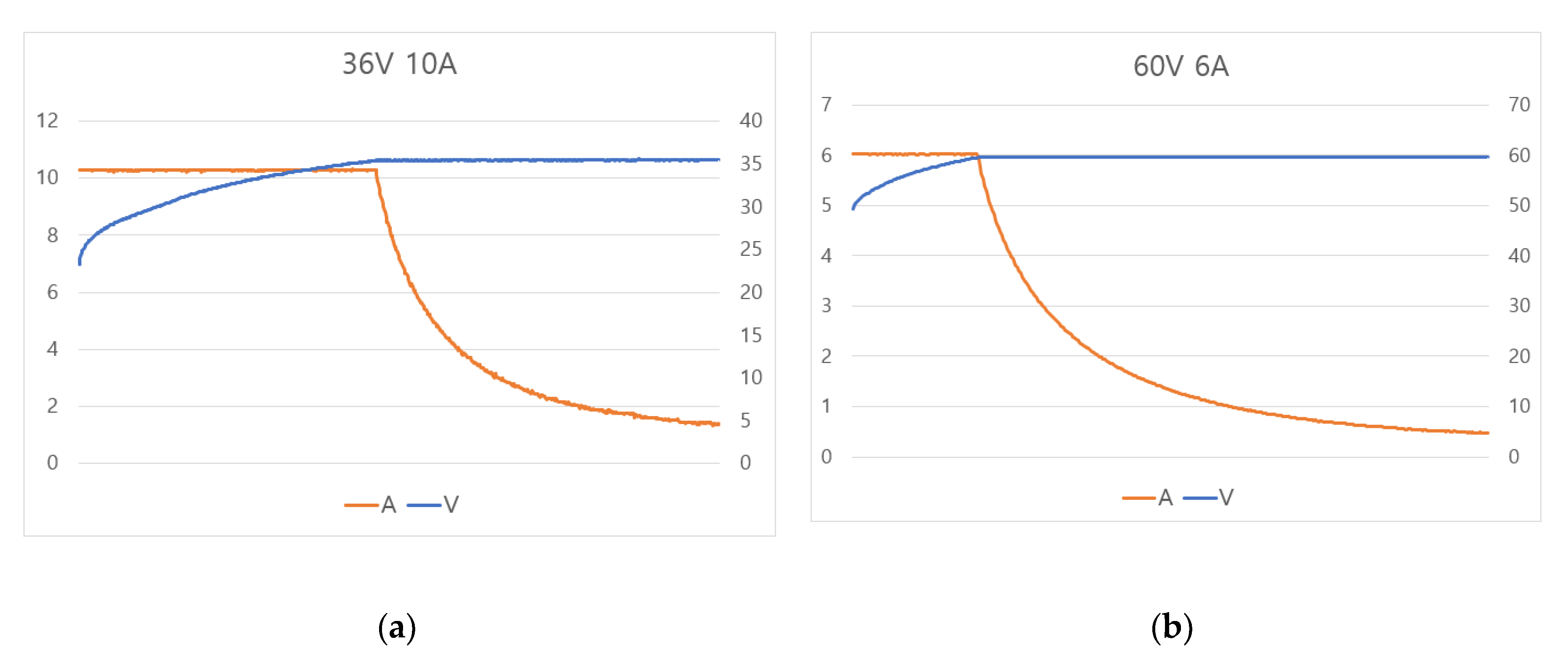
3.1. Simulation

Figure 11 shows the simulation circuits used to verify the validity of the proposed DPS-MLC. The circuits consist of the existing buck converter, the DSS-MLC, and the proposed DPS-MLC. To facilitate the verification of the size of the current through the reactor and the ripple rate, a reactance value was designed for the switching of the reactor current in the continuous mode. To compare the characteristics of a general buck converter and the two topologies, the parameters of the passive elements used for the simulation were designed as identical values. The parameters used in this simulation are listed in Table 2.
Figure 12 shows the voltage and reactor current waveforms obtained by PWM (Pulse Width Modulation) using the existing buck converter and the two multilevel converters. First, to verify the reactor current ripple and PWM voltage ripple according to each voltage region, the voltage and current were simulated so as to increase linearly from 0 V to 70 V and from 0 A to 12 A, respectively, for all three converters.
As indicated by the simulation waveforms, the proposed DPS-MLC considerably decreases the voltage and output current ripples by PWM when compared to the existing single buck converter. In addition, the voltage and output current ripples of the proposed DPS-MLC are the same as those of the DSS-MLC.
Figure 13 shows the simulation results of the output voltage drops for the existing single buck converter and two multilevel converters in terms of the diode voltage drop. The simulation conditions were as follows: the duty ratio was linearly increased from 0 to 100% for each level, and the level was increased from 1 to 6 to compare the output voltages between the two multilevel converters and the single buck converter. As can be seen from the resulting waveforms, the DSS-MLC generates the largest difference in the output voltage at level 1, and the output voltage decreases as the number of levels of the converter increases. Furthermore, in the level 1 converter mode, the output voltage is not generated because of the diode voltage drop at a low duty ratio. The DPS-MLC exhibits a constant voltage drop regardless of the number of levels of the converter, and the voltage drop caused by the diode disappears when the number of levels of the converter is at a maximum. The proposed DPS-MLC exhibits an improvement in the output voltage drop caused by the diode and can generate an output at level 1 even at a low duty ratio.
Figure 14 shows the battery charge simulation waveforms of the charging system composed of the existing buck converter and the charging systems composed of the two types of multilevel converters. Here, Vob, Vo_DSS, and Vo_DPS denote output voltage of the existing single buck converter, output voltage of DSS-MLC, and output voltage of DPS-MLC. And they have all the same condition with duty 50%. The Randles model was used for the battery equivalent circuit, and the parasitic inductance at the battery terminal caused by a high frequency was ignored. For a smooth simulation, the battery equivalent model was configured by assuming a charge start voltage of 55 V and a charge stop voltage of 60 V. The model was operated in the CC-CV mode during the charging section, and the current reference value in the CC mode was set to 8 A.
Figure 14a shows the results of the battery charge simulation for the single buck converter. The current ripple Δ i L is approximately 2.45 A, and the current ripple rate is 30.6%. Figure 14b shows the results of the battery charge simulation for the DSS-MLC. The current ripple Δ i L is 0.3 A on average, and the current ripple rate is 3.7%. Figure 14c shows the results of the battery charge simulation for the DPS-MLC. Here, the current ripple rate is almost the same as that of the DSS-MLC in all the sections and is reduced eightfold when compared to that of the single buck converter.
The simulation results show that the DPS-MLC reduces the current ripples in all the charging regions when compared to the existing single buck converter. The DPS-MLC shows the same current ripple rate as the DSS-MLC and a lower voltage drop caused by the diode than the DSS-MLC. Therefore, the DPS-MLC can respond to a broader range of charging voltages. Furthermore, a more efficient operation of the charging system is possible because of the small switching loss caused by the diode.

3.2. Experiment

To verify the operation of the proposed DPS-MLC, a charging system was fabricated, as shown in Figure 15. It was composed of 1000-W-class multilevel converters with six levels in total, a controller with a DSP, and a multilevel power supply using a switched-mode power supply (SMPS). The six converters were controlled using the onboard-type TMS320F28027 kit, and the size of the multilevel charging board was minimized.
In this study, experiments were performed to compare the operational characteristics of the proposed DPS-MLC with those of a single buck converter. A resistance load was used instead of the battery load to observe the dynamic characteristics when the number of levels changed while controlling the output voltage continuously from the minimum value to the maximum level. For a stable output voltage control, the output capacitor was designed to be 220 µF. The other parameter conditions are listed in Table 3.
For the experimental conditions, the controller and voltage ref were designed in such a way that the output voltage would increase linearly with the same time constant from 0 V to 70 V. Among the operational characteristics of the two converters, the PWM output voltage ripple and reactor current ripple were observed.
On Figure 16 for ch1: yellow shows the waveforms resulting from the experiment when using the reactor current ripple, and for ch2: green shows voltage V P W M obtained by PWM. As can be seen from the experimental waveforms, the DPS-MLC achieves a stable control even in the section where the number of levels changes, and the current ripple is also constant regardless of the level. Furthermore, the current ripple of the multilevel converter decreases in every region when compared to that of the single buck converter. In addition, the voltage ripple obtained by PWM is also small and is 16.7% of that of the single buck converter. Thus, the DPS-MLC is expected to generate fewer instances of electromagnetic interference caused by switching.
Figure 17 shows the experimental charging waveforms for the proposed topology. The experimental conditions were as follows: two battery voltages (36 and 60 V) were used, and a CC-CV control was used for the charging method. The battery charge voltage and current data were collected using the data logger midi LOGGER GL240. Variations in the voltage and current were recorded over time and represented as a graph. As shown in the figure, the experimental results confirm that the proposed topology charges e-mobility devices with various charge voltages.
Figure 18 shows the experimental results comparing the proposed topology with existing topologies. The experimental conditions were as follows: a 1-kW-class SMPS with an efficiency of approximately 90% was used. The charging current was set to 16.7 A, and the power was measured in 150-W units using the power analyzer WT-3000 while increasing the charging voltage from 12 V to 72 V. As can be seen from the obtained waveforms, the proposed DPS-MLC has the highest efficiency at 750 W in every section excluding the single buck converter. The result for 150 W, which is a low charging voltage region where the efficiency difference is large, shows that the efficiencies of the general buck converter, DSS-MLC, and DPS-MLC are 73.1%, 87.5%, and 88.5%, respectively. Thus, the efficiency of the DPS-MLC is 15.1% higher than that of the general buck converter and 0.7% higher than that of the DSS-MLC. This demonstrates that the DPS-MLC exhibits an improved efficiency while maintaining the advantages of a multilevel converter for various charging voltages.

4. Conclusions

Various charging technologies are being researched and developed for e-mobility devices. This paper proposed a new topology for a charging system for e-mobility devices. The validity of the proposed multilevel charging system was verified through simulations and experiments. The conclusions of this study can be summarized as follows:
  • The DPS-MLC exhibits an improved efficiency by reducing the switching loss of the diode while providing the same operational characteristics as the existing multilevel converter DSS-MLC. The serial connection structure of the diodes at the output side of the multilevel design is changed to a parallel connection structure. Therefore, the loss can be reduced regardless of the number of levels by using only one output diode in the freewheeling switching section.
  • The voltage drop caused by the diode is minimized to increase the control region of the charging voltage. This region, which can be responsible for each multilevel converter, is expanded to a wider range. As the number of multilevel converters increases, the advantages of the DPS-MLC become more prominent. However, the operation of the DSS-MLC is limited because the voltage drop caused by the diode increases at a lower level. The DPS-MLC solves this problem and can control a wide range of charging voltages regardless of the number of levels. In particular, it has a high efficiency when compared to DSS-MLC in the low output voltage section. It is more advantageous in the PMD field because the charging voltage range of the PMD is from 12 V to 36 V.
  • The DPS-MLC has a considerably better efficiency than the single buck converter and can improve the charging power quality by reducing the current ripple. Furthermore, it can also reduce the electromagnetic interference caused by the charging system by reducing the voltage ripples obtained by PWM.
Therefore, the proposed multilevel charging system improves existing multilevel charging systems. It is expected to make great contributions to the field of charging technology and enable e-mobility devices to be established as short-distance mobile transportation vehicles.

Author Contributions

Software, writing—review, formal analysis, and writing-original draft, J.-H.L.; Funding acquisition, and resources, S.-J.P.; Supervision and project administration, S.-K.L. All authors have read and agreed to the published version of the manuscript.

Funding

This study was supported by research fund from Honam University, 2020.

Conflicts of Interest

The authors declare no conflict of interest.

References

  1. Rigas, E.S.; Ramchurn, S.D.; Bassiliades, N.; Koutitas, G. Congestion Management for Urban EV Charging Systems. In Proceedings of the 2013 IEEE International Conference on Smart Grid Communications (SmartGridComm), Vancouver, BC, Canada, 21–24 October 2013; pp. 121–126. [Google Scholar]
  2. ElBanhawy, E.Y. Investigating the evolution of e-mobility in its urban context a longitudinal study in Newcastle-Gateshead area. In Proceedings of the 5th IET Hybrid and Electric Vehicles Conference (HEVC 2014), London, UK, 5–6 November 2014; pp. 1–11. [Google Scholar]
  3. Creutzig, F.; Baiocchi, G.; Bierkant, R.; Seto, K.C. Global typology of urban energy use and potentials for an urbanization mitigation wedge. Proc. Natl. Acad. Sci. USA 2015, 112, 6283–6288. [Google Scholar] [CrossRef] [PubMed] [Green Version]
  4. Momirlan, M.; Veziroglu, T. The properties of hydrogen as fuel tomorrow in sustainable energy system for a cleaner planet. Int. J. Hydrogen Energy 2005, 30, 795–802. [Google Scholar] [CrossRef]
  5. Li, C.; Cao, Y.; Zhang, M.; Wang, J.; Liu, J.; Shi, H.; Geng, Y. Hidden Benefits of Electric Vehicles for Addressing Climate Change. Sci. Rep. 2015, 5, 9213. [Google Scholar] [CrossRef] [PubMed] [Green Version]
  6. Hawkins, T.R.; Singh, B.; Majeau-Bettez, G.; Strømman, A.H. Comparative environmental life cycle assessment of conventional and electric vehicles. J. Ind. Ecol. 2013, 17, 53–64. [Google Scholar] [CrossRef]
  7. Ahmad, F.; Alam, M.S.; Asaad, M. Developments in xEVs charging infrastructure and energy management system for smart microgrids including xEVs. Sustain. Cities Soc. 2017, 35, 552–564. [Google Scholar] [CrossRef]
  8. Schlund, J.; Steinert, R.; Pruckner, M. Coordinating E-Mobility charging for frequency containment reserve power provision. In Proceedings of the e-Energy ’18: The Ninth International Conference on Future Energy Systems, Karlsruhe, Germany, 12–15 June 2018; pp. 556–563. [Google Scholar]
  9. Deventer, P.; Steen, M.; Schelven, R.; Rubin, B.; Kotter, R. Large-Scale Deployment of Public Charging Infrastructure: Identifying Possible Next Steps Forward; Springer International Publishing: Berlin/Heidelberg, Germany, 2015; pp. 107–124. [Google Scholar]
  10. Nikulina, V.; Simon, D.; Ny, H.; Baumann, H. Context-adapted urban planning for rapid transitioning of personal mobility towards sustainability: A systematic literature review. Sustainability 2019, 11, 1007. [Google Scholar] [CrossRef] [Green Version]
  11. Kaya, K.; Poyrazoglu, G. A Platform for Personal E-Mobility with Route Forecasting. In Proceedings of the 2020 International Conference on Electrical, Communication, and Computer Engineering (ICECCE), Istanbul, Turkey, 12–13 June 2020; pp. 1–5. [Google Scholar]
  12. Kuo, J.Y.; Sayeed, A.; Tangirala, N.T.; Han, V.C.Y.; Dauwels, J.; Mayer, M.P. Pedestrians’ acceptance of personal mobility devices on the shared path: A structural equation modelling approach. In Proceedings of the 2019 IEEE Intelligent Transportation Systems Conference (ITSC), Auckland, New Zealand, 27–30 October 2019; pp. 2349–2354. [Google Scholar]
  13. Thomas, D.; Klonari, V.; Vallée, F.; Ioakimidis, C.S. Implementation of an e-bike sharing system: The effect on low voltage network using pv and smart charging stations. In Proceedings of the 2015 International Conference on Renewable Energy Research and Applications (ICRERA), Palermo, Italy, 22–25 November 2015; pp. 572–577. [Google Scholar]
  14. Mauromicale, G.; Raciti, A.; Rizzo, S.A.; Susinni, G.; Parise, G.; Parise, L. E-mobility: Safety, Service Continuity and Penetration of Charging Systems. In Proceedings of the 2019 AEIT International Conference of Electrical and Electronic Technologies for Automotive (AEIT AUTOMOTIVE), Torino, Italy, 2–4 July 2019; pp. 1–6. [Google Scholar]
  15. Ivan, P.; Hrvoje, P.; Tomislav, C. Electric vehicle based smart e-mobility system–Definition and comparison to the existing concept. Appl. Energy 2020, 272, 115153. [Google Scholar]
  16. Lim, S.; Lee, H.; Cha, H.; Park, S. Multi-Level DC/DC Converter for E-Mobility Charging Stations. IEEE Access 2020, 8, 48774–48783. [Google Scholar] [CrossRef]
  17. Dimitrov, B.; Hayatleh, K.; Barker, S.; Collier, G.; Sharkh, S.; Cruden, A. A Buck-Boost Transformerless DC–DC Converter Based on IGBT Modules for Fast Charge of Electric Vehicles. Electronics 2020, 9, 397. [Google Scholar] [CrossRef] [Green Version]
  18. Abronzini, U.; Attaianese, C.; D’Arpino, M.; Di Monaco, M.; Genovese, A.; Pede, G.; Tomasso, G. Multi-source power converter system for EV charging station with integrated ESS. In Proceedings of the 2015 IEEE 1st International Forum on Research and Technologies for Society and Industry Leveraging a Better Tomorrow (RTSI), Turin, Italy, 16–18 September 2015; pp. 427–432. [Google Scholar]
  19. Dahidah, M.S.A.; Liu, H.; Agelidis, V.G. Reconfigurable Converter with Multiple-Voltage Multiple-Power for E-Mobility Charging. In Proceedings of the 2018 International Power Electronics Conference (IPEC-Niigata 2018-ECCE Asia), Niigata, Japan, 20–24 May 2018; pp. 3215–3222. [Google Scholar]
  20. Kesler, M.; Kisacikoglu, M.C.; Tolbert, L.M. Vehicle-to-Grid Reactive Power Operation Using Plug-In Electric Vehicle Bidirectional Offboard Charger. IEEE Trans. Ind. Electron. 2014, 61, 6778–6784. [Google Scholar] [CrossRef]
  21. Malik, M.Z.; Chen, H.; Nazir, M.S.; Khan, I.A.; Abdalla, A.N.; Ali, A.; Chen, W. A New Efficient Step-Up Boost Converter with CLD Cell for Electric Vehicle and New Energy Systems. Energies 2020, 13, 1791. [Google Scholar] [CrossRef] [Green Version]
  22. Huang, W.; Abu Qahouq, J.A. Input Voltage Ripple-Based Sensorless Current Sharing Autotuning Controller for Multiphase DC–DC Converters. IEEE Trans. Ind. Appl. 2016, 52, 4117–4125. [Google Scholar] [CrossRef]
  23. Ferreira, J.A. The Multilevel Modular DC Converter. IEEE Trans. Power Electron. 2013, 28, 4460–4465. [Google Scholar] [CrossRef]
  24. Nguyen, M.K.; Choi, Y.O. Voltage Multiplier Cell-Based Quasi-Switched Boost Inverter with Low Input Current Ripple. Electronics 2019, 8, 227. [Google Scholar] [CrossRef] [Green Version]
  25. Ismail, A.A.A.; Elnady, A. Advanced Drive System for DC Motor Using Multilevel DC/DC Buck Converter Circuit. IEEE Access 2019, 7, 54167–54178. [Google Scholar] [CrossRef]
  26. Thinh, Q.; Ngoc, C.; Lee, S.H.; Kim, S.M.; Kim, H.C.; Eel, H. Analyzing Modulation Techniques for the Modular Multilevel Converter. Int. J. Comput. Electr. Eng. 2016, 8, 259–271. [Google Scholar] [CrossRef] [Green Version]
  27. Babaei, E. A Cascade Multilevel Converter Topology with Reduced Number of Switches. IEEE Trans. Power Electron. 2008, 23, 2657–2664. [Google Scholar] [CrossRef]
  28. Prozorov, A.M.; Nikitin, D.A.; Tarasov, A.D. Techniques for reducing output current ripple in a flyback converter with PFC. In Proceedings of the 2019 Ural Symposium on Biomedical Engineering, Radioelectronics and Information Technology (USBEREIT), Yekaterinburg, Russia, 25–26 April 2019; pp. 391–393. [Google Scholar]
  29. Xiong, Y.; Sun, S.; Jia, H.; Shea, P.; John Schen, Z. New Physical Insights on Power MOSFET Switching Losses. IEEE Trans. Power Electron. 2009, 24, 525–531. [Google Scholar] [CrossRef]
  30. Bazzi, A.M.; Krein, P.T.; Kimball, J.W.; Kepley, K. IGBT and Diode Loss Estimation under Hysteresis Switching. IEEE Trans. Power Electron. 2012, 27, 1044–1048. [Google Scholar] [CrossRef]
  31. Chen, J.; Zhu, J.; Guo, Y. Calculation of Power Loss in Output Diode of a Flyback Switching DC-DC Converter. In Proceedings of the 2006 CES/IEEE 5th International Power Electronics and Motion Control Conference, Shanghai, China, 14–16 August 2006; pp. 1–5. [Google Scholar]
  32. Jiang, H.; Wei, J.; Dai, X.; Ke, M.; Zheng, C.; Deviny, I. Silicon carbide split-gate MOSFET with merged Schottky barrier diode and reduced switching loss. In Proceedings of the 2016 28th International Symposium on Power Semiconductor Devices and ICs (ISPSD), Prague, Czech Republic, 12–16 June 2016; pp. 59–62. [Google Scholar]
  33. Xu, Y.; Ho, C.N.M.; Ghosh, A.; Muthumuni, D. An Electrical Transient Model of IGBT-Diode Switching Cell for Power Semiconductor Loss Estimation in Electromagnetic Transient Simulation. IEEE Trans. Power Electron. 2020, 35, 2979–2989. [Google Scholar] [CrossRef]
Figure 1. Growing urban population and increasing number of cities. * UN World Urbanization Prospects, POSRI (2017).
Electronics 09 02037 g001
Figure 2. Topology of the existing diode series structure multilevel converter (DSS-MLC).
Electronics 09 02037 g002
Figure 3. Topology of the proposed diode parallel structure multilevel converter (DPS-MLC).
Electronics 09 02037 g003
Figure 4. Operational state of DSS-MLC according to the switching state.
Electronics 09 02037 g004
Figure 5. Operational state of DPS-MLC according to the switching state.
Electronics 09 02037 g005
Figure 6. Normalized input ripple current versus duty cycle.
Electronics 09 02037 g006
Figure 7. Normalized output current ripple versus duty cycle.
Electronics 09 02037 g007
Figure 8. V T H and R D values according to T v j .
Electronics 09 02037 g008
Figure 9. Reverse recovery characteristics of the diode.
Electronics 09 02037 g009
Figure 10. Output characteristics considering the diode voltage drop.
Electronics 09 02037 g010
Figure 11. Simulation circuit diagram.
Electronics 09 02037 g011
Figure 12. Comparison between the operational output characteristics of the existing converter and proposed converter.
Electronics 09 02037 g012
Figure 13. Comparison between the output voltages of the existing converter and proposed converter: (a) output voltage waveforms of three converters (b) differences between the output voltages of three converters.
Electronics 09 02037 g013
Figure 14. Comparison between the battery charge simulation results of the (a) buck converter, (b) DSS-MLC, and (c) DPS-MLC.
Electronics 09 02037 g014
Figure 15. DPS-MLC used for the experiment.
Electronics 09 02037 g015
Figure 16. Current ripples of the reactor and voltage waveforms obtained by PWM for the (a) buck converter and (b) DPS-MLC.
Electronics 09 02037 g016
Figure 17. Battery charging results for (a) 36 V/10 A and (b) 60 V/6 A.
Electronics 09 02037 g017
Figure 18. Comparison between the efficiency curves of three topologies.
Electronics 09 02037 g018
Table 1. Output voltages according to the switching state in each mode.
Q1Q2Q3DSS-MLC V M L DPS-MLC V M L
Mode 100000
Mode 2100 V i M L V i M L
Mode 3110 2 × V i M L 2 × V i M L
Mode 4111 3 × V i M L 3 × V i M L
Table 2. Specifications and parameters of the simulation circuits.
ParameterSymbolValue
Buck converter input voltageVinb72 V
Multilevel converter input voltageV1V612 V
Output reactor inductanceRL1, RL3, RL4200 μH
Output capacitor capacitanceCb, Cdss, Cdps10 μF
Output load resistanceRload6 Ω
Switching frequencyfs20 kHz
Table 3. Specifications and parameters of the experiment.
ParameterValue
Output inductor inductance200 μH
Output capacitor capacitance220 μF
Output load resistance13.5 Ω
Switching frequency20 kHz
Publisher’s Note: MDPI stays neutral with regard to jurisdictional claims in published maps and institutional affiliations.

