X-Type Step-Up Multi-Level Inverter with Reduced Component Count Based on Switched-Capacitor Concept

 ,
,  ,
,  ,
,  ,
, 
 ,
,  and
and
Abstract
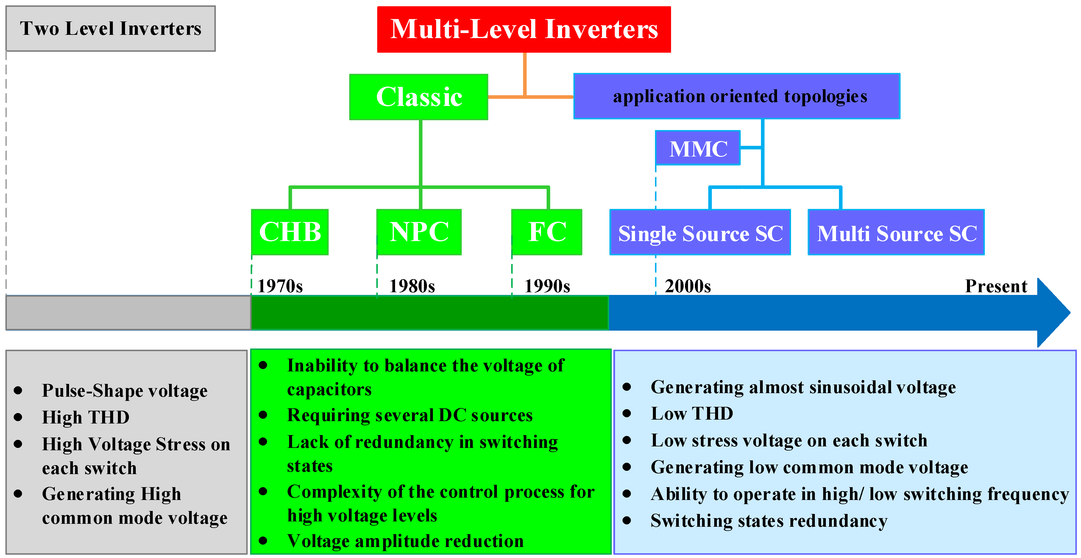
1. Introduction
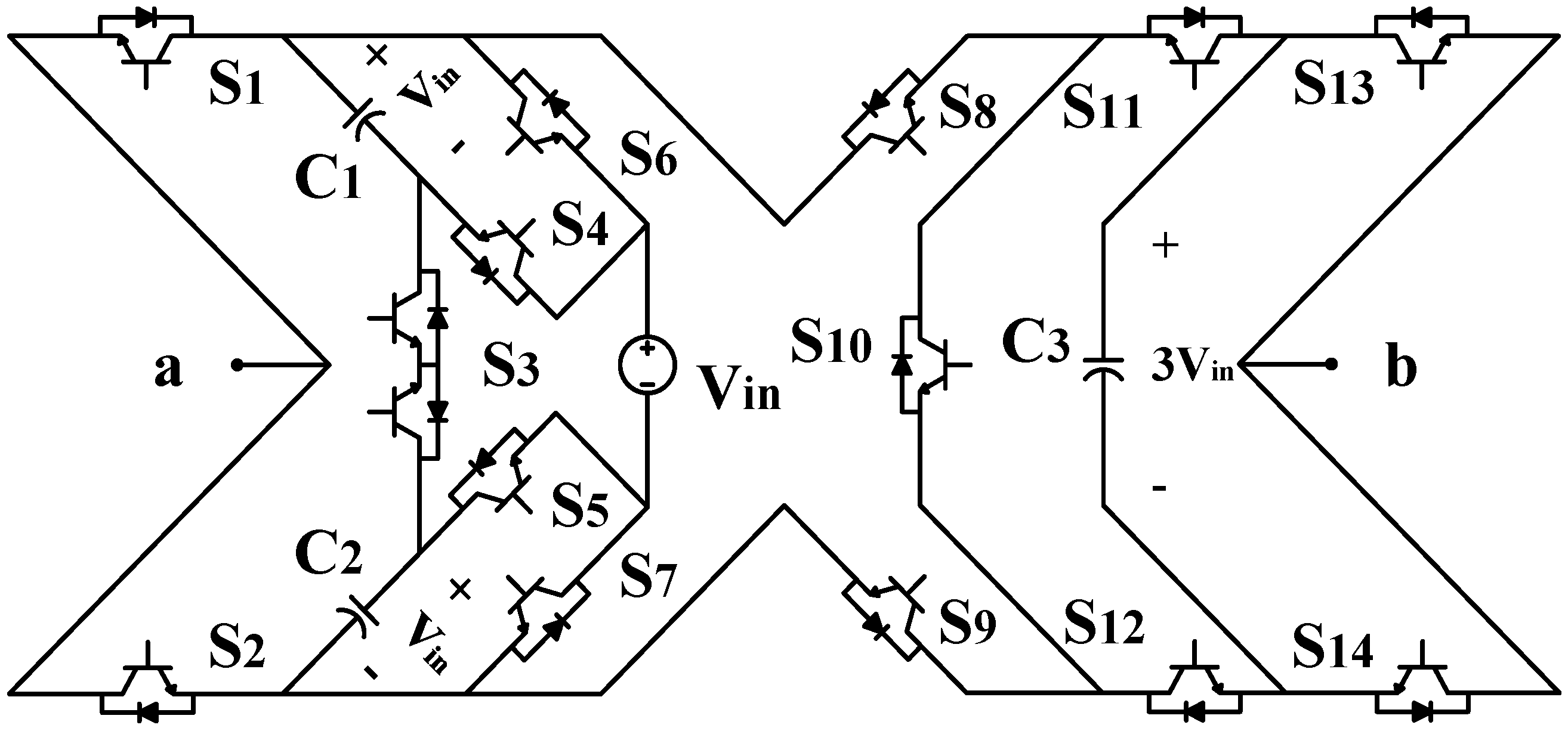
2. Proposed Topology: Structure and Operating Principals
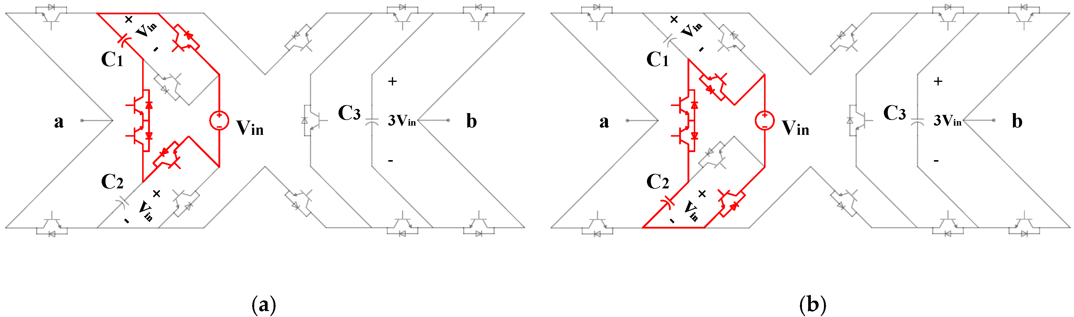
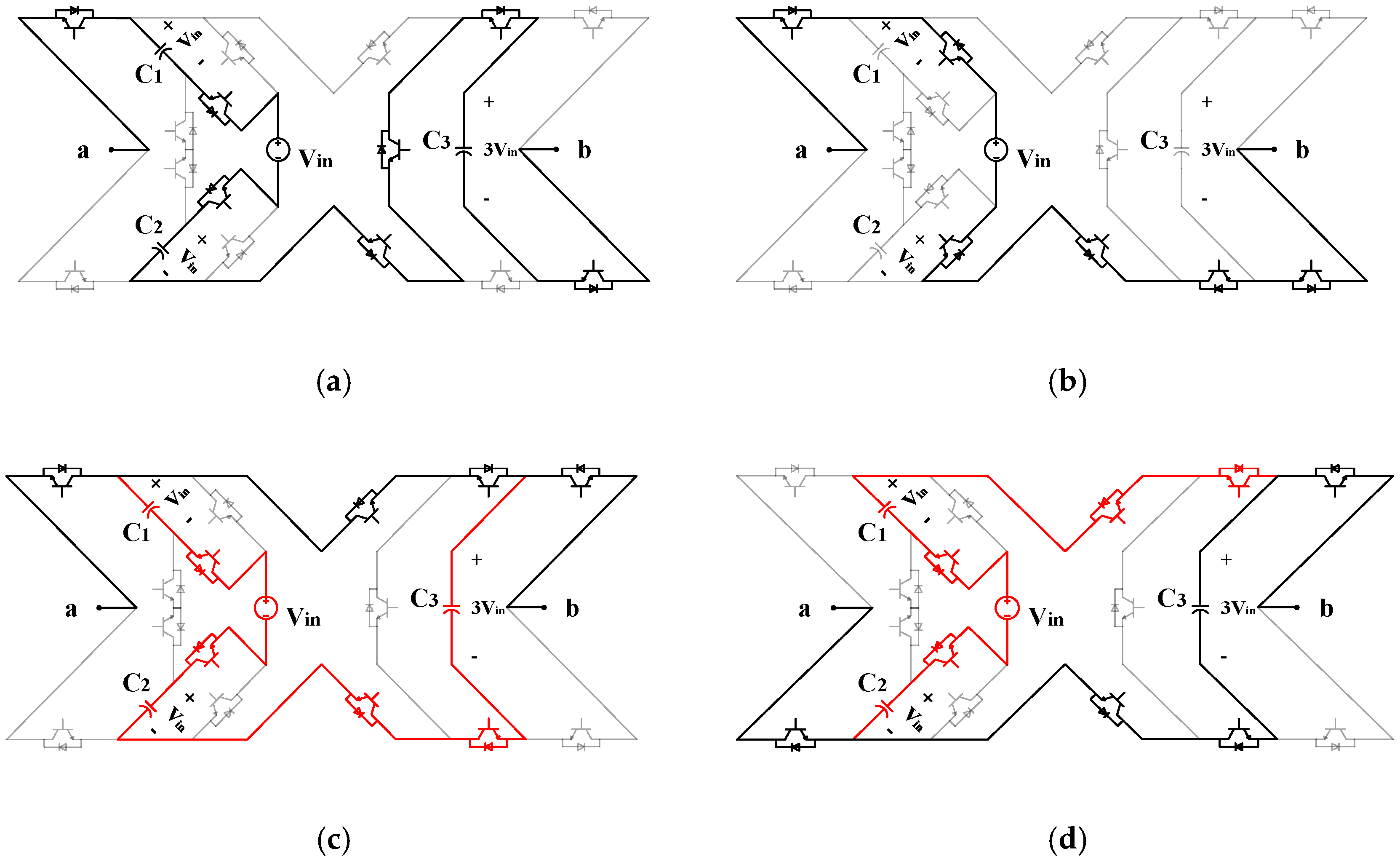
- Level +6Vdc: Figure 4a illustrates the current path for generating this level. Capacitors C1, C2, and C3 are discharged across the load in series with the input source.
- Level +5Vdc: Two different switching states can be used to make this level. One is through the series connection of C1, C3, and DC source while charging C2 simultaneously. The other is through series connection of C2, C3, and DC source while charging C1 simultaneously.
- Level +4Vdc: C3 and DC source make this level together.
- Level +3Vdc: This level is built with the help of C1 and C2 along with the DC source. Moreover, C3 can be charged at the same time.
- Level +2Vdc: To make this level, there are two switching states. First, C1 is discharged across the load with the DC source and at the same time C2 is charged. Second, the capacitor C2 and the input source supply the load and simultaneously C1 is charged.
- Level +1Vdc: The voltage source is only used to make this voltage level (Figure 4b).
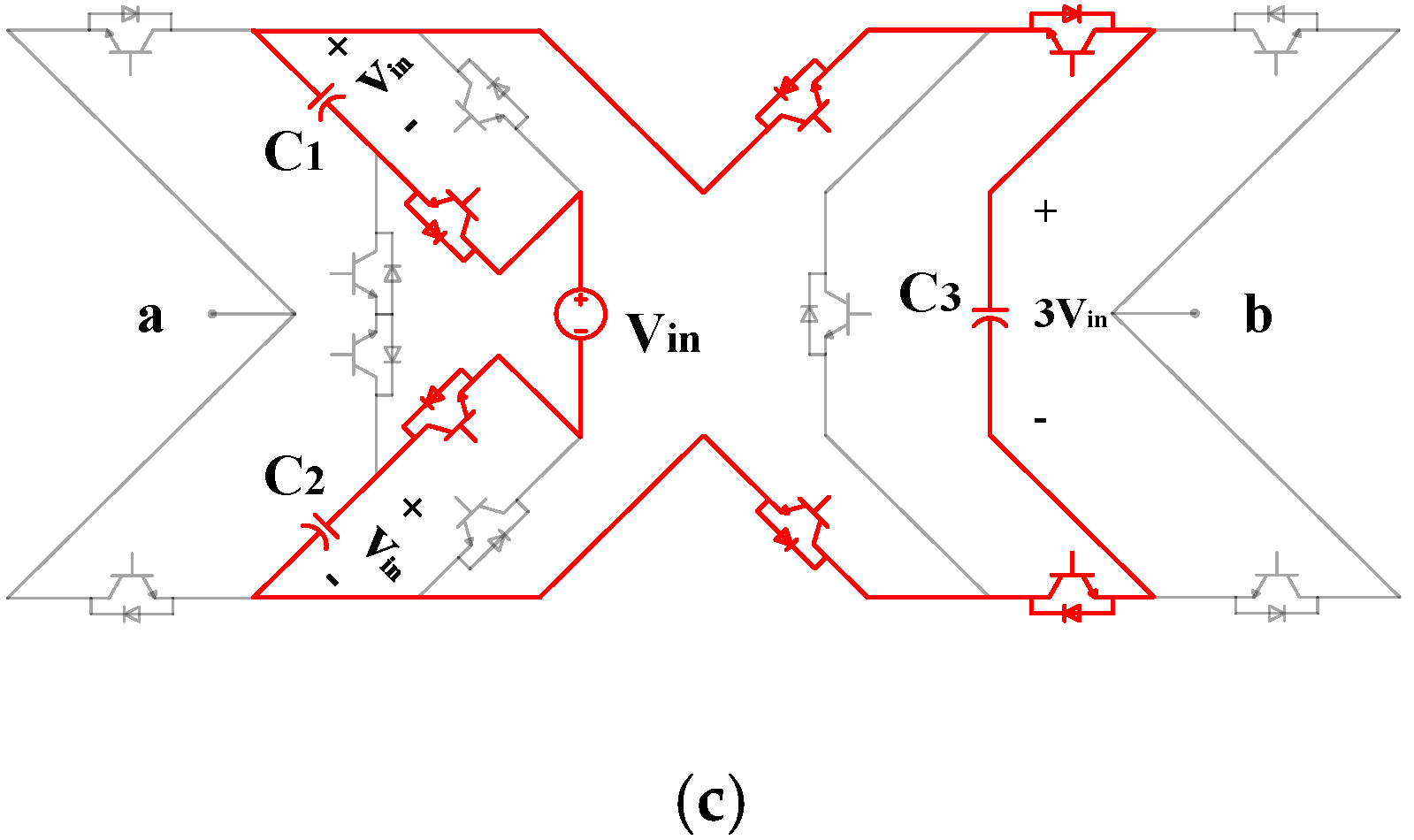
- Level zero: There are two switching states to form the level zero: First by turning the S1, S8, S11, and S13 switches on. Second using the switches S2, S9, S12, and S14. Moreover, C3 can be charged through the C1, C2, and DC source, as shown in Figure 4c.
- Negative voltage levels of −1Vdc, −2Vdc, …, −6Vdc are obtained similarly.
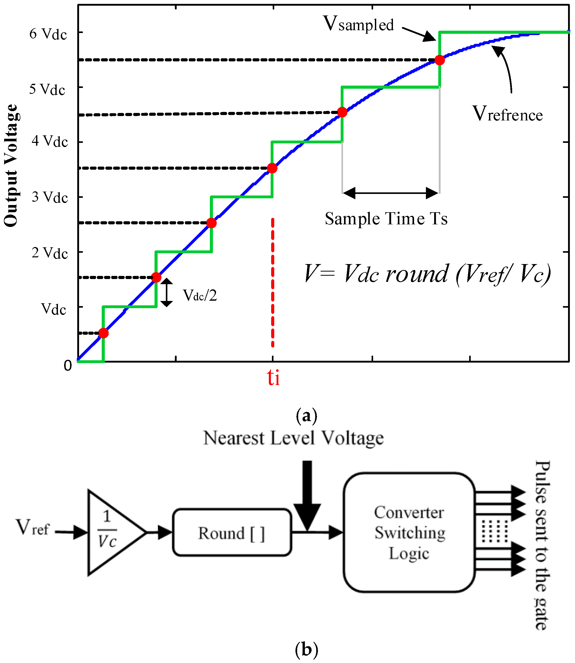
2.1. Modulation Strategy
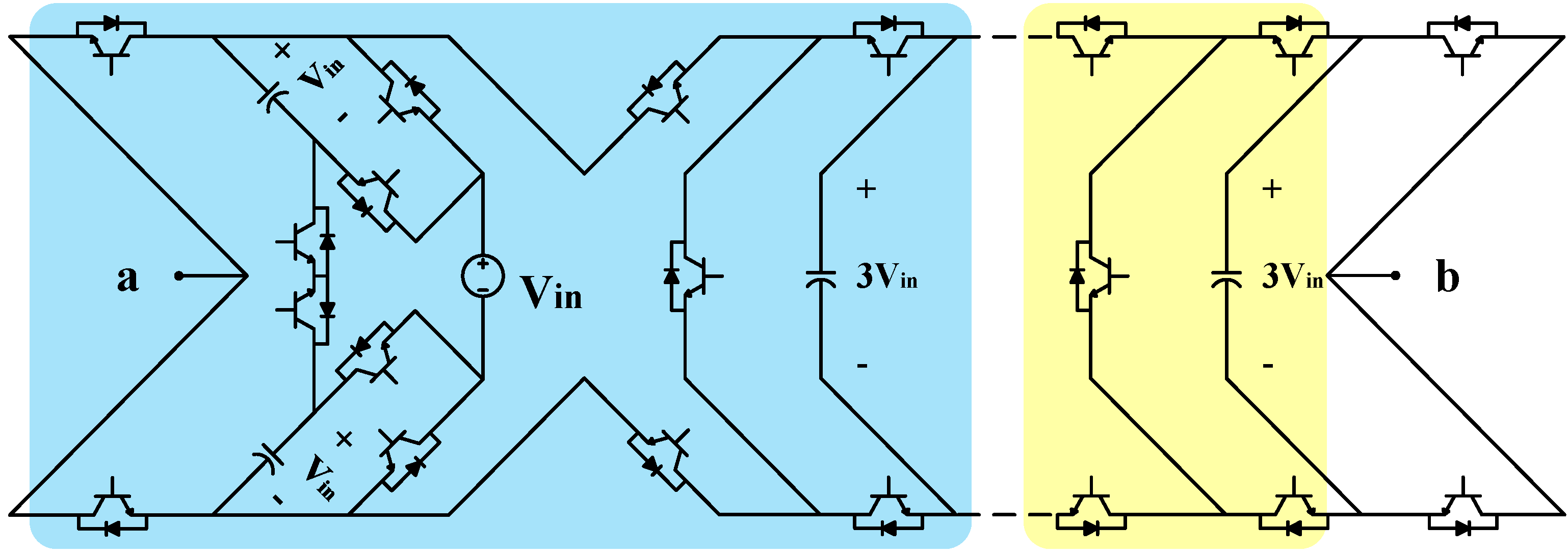
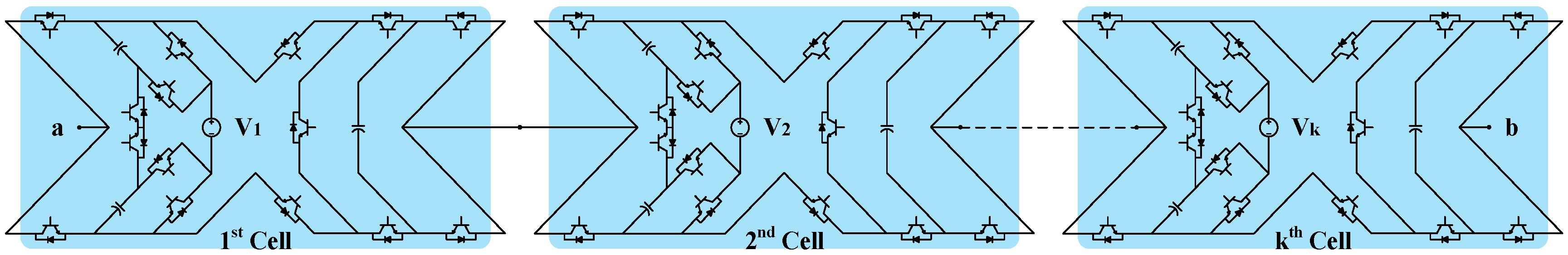
2.2. Extended Topology
3. Discussion
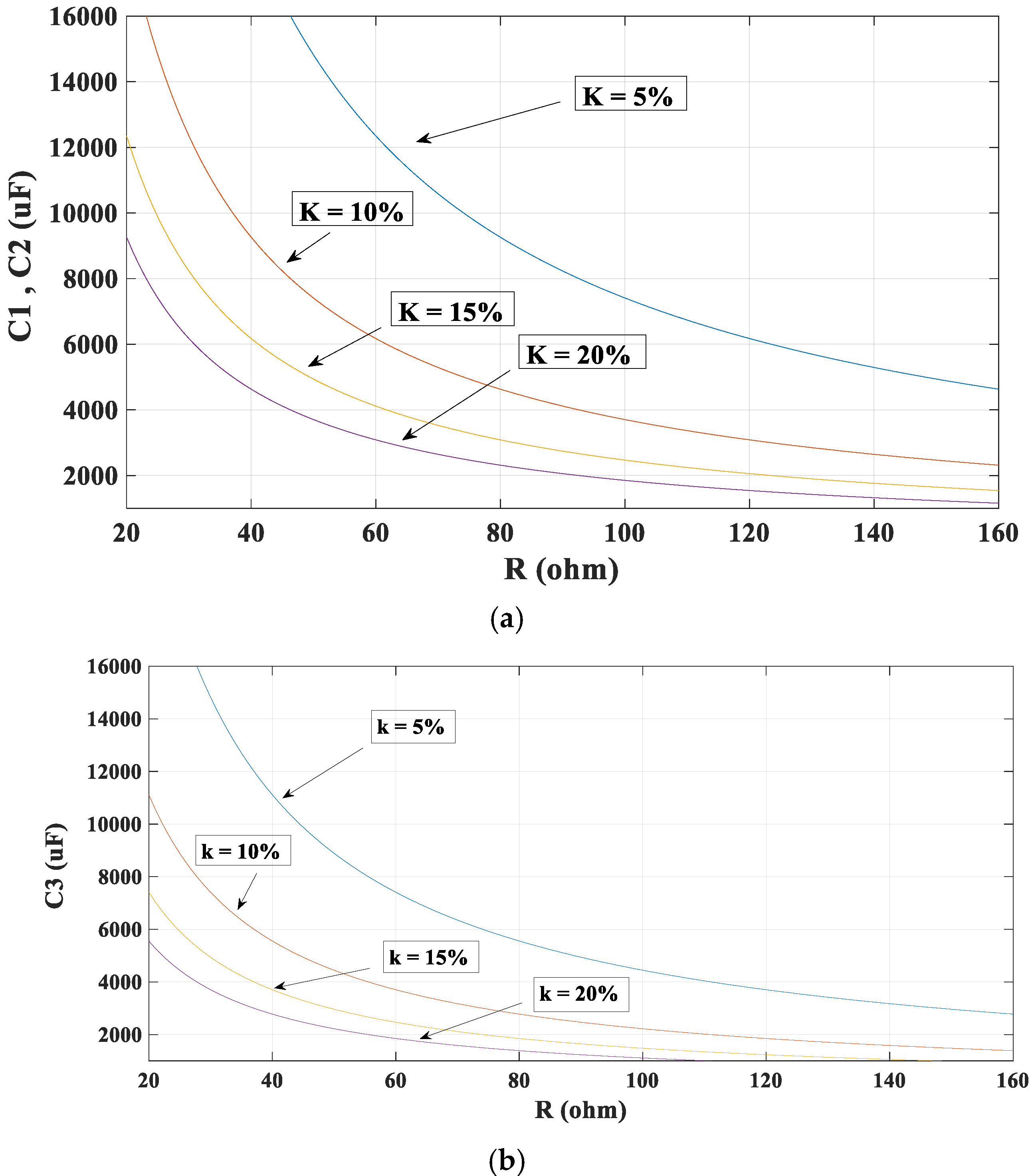
3.1. Determination of Capacitance
3.2. Power Loss Analysis
3.2.1. Switching Losses
3.2.2. Conduction Losses
3.2.3. Losses Due to the Capacitors Voltage Ripple
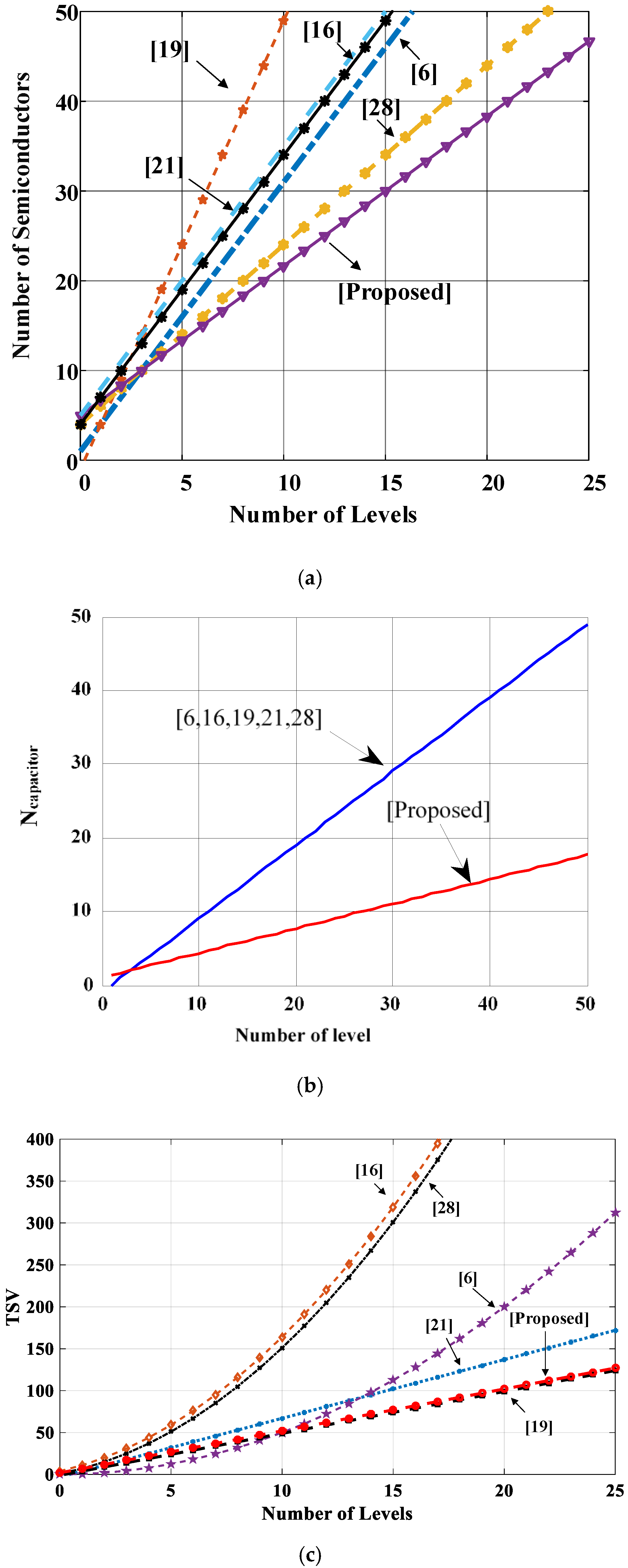
3.3. Comparative Study
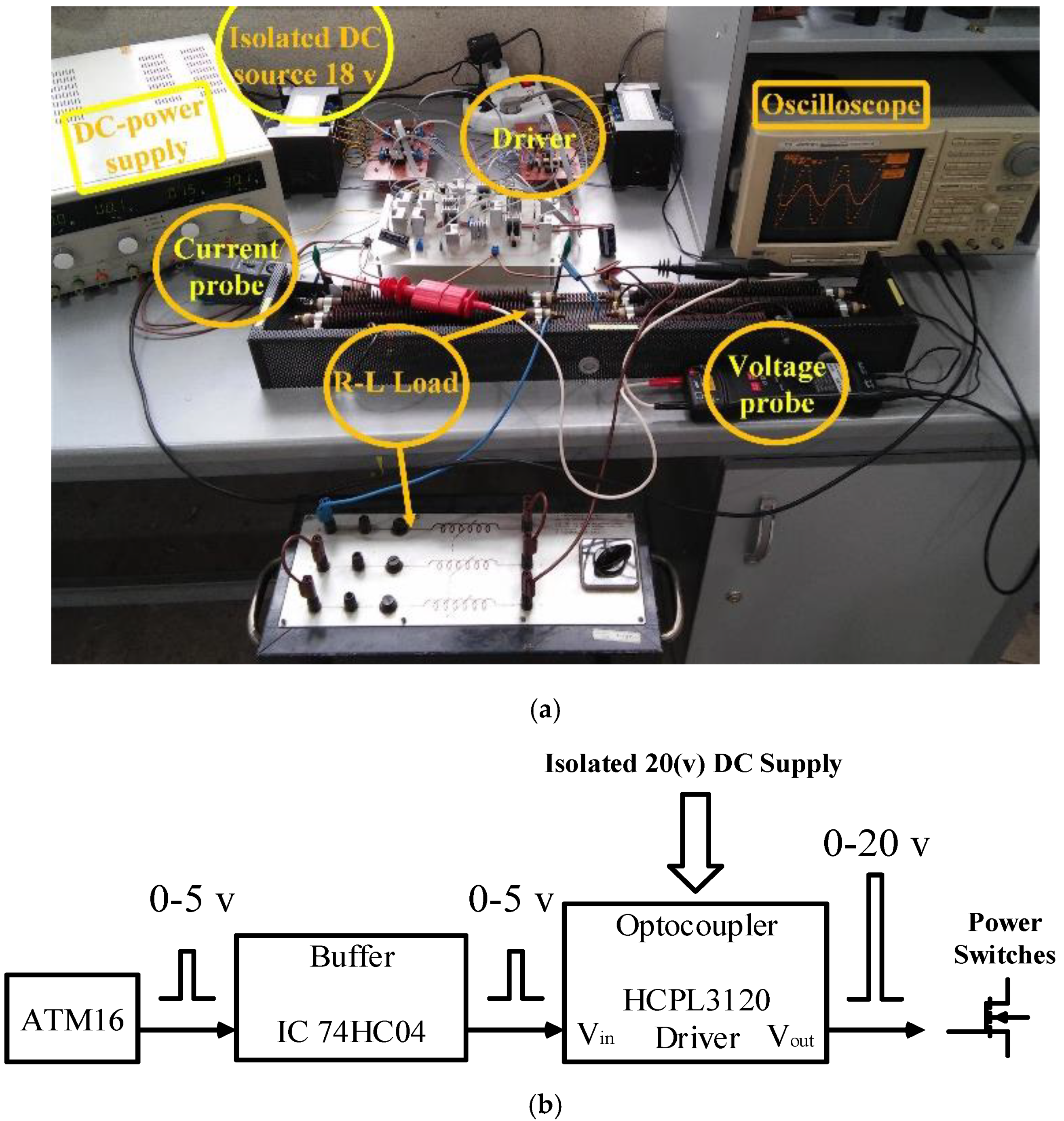
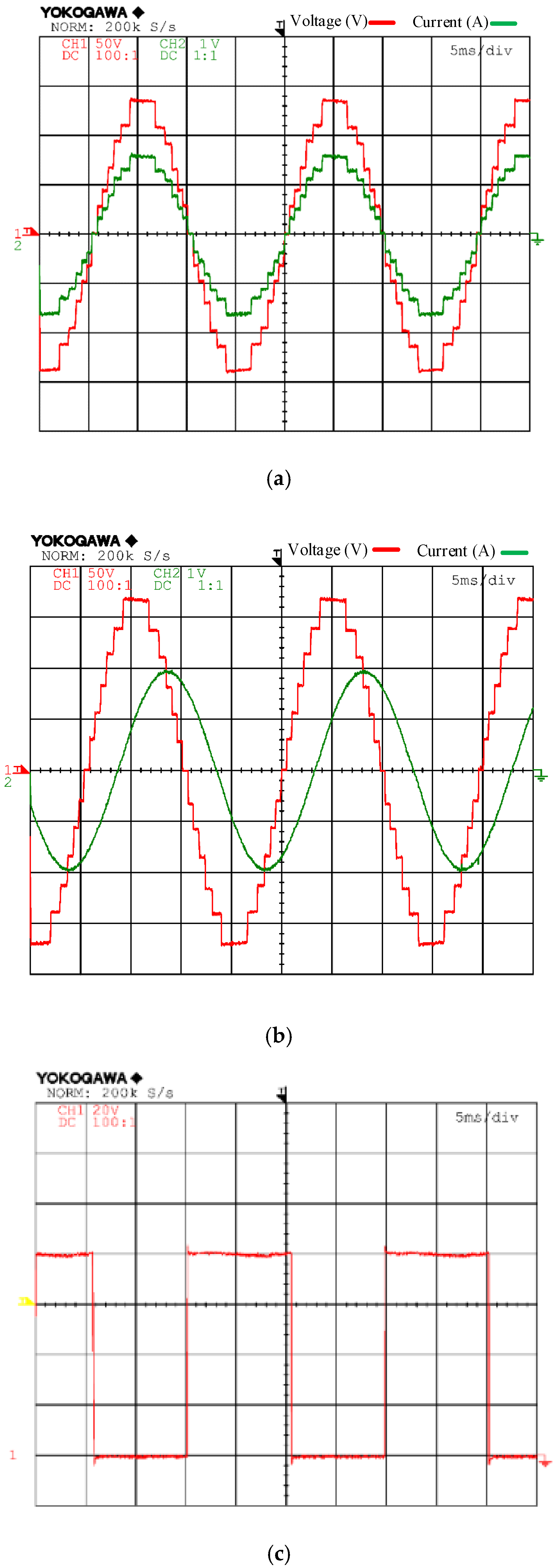
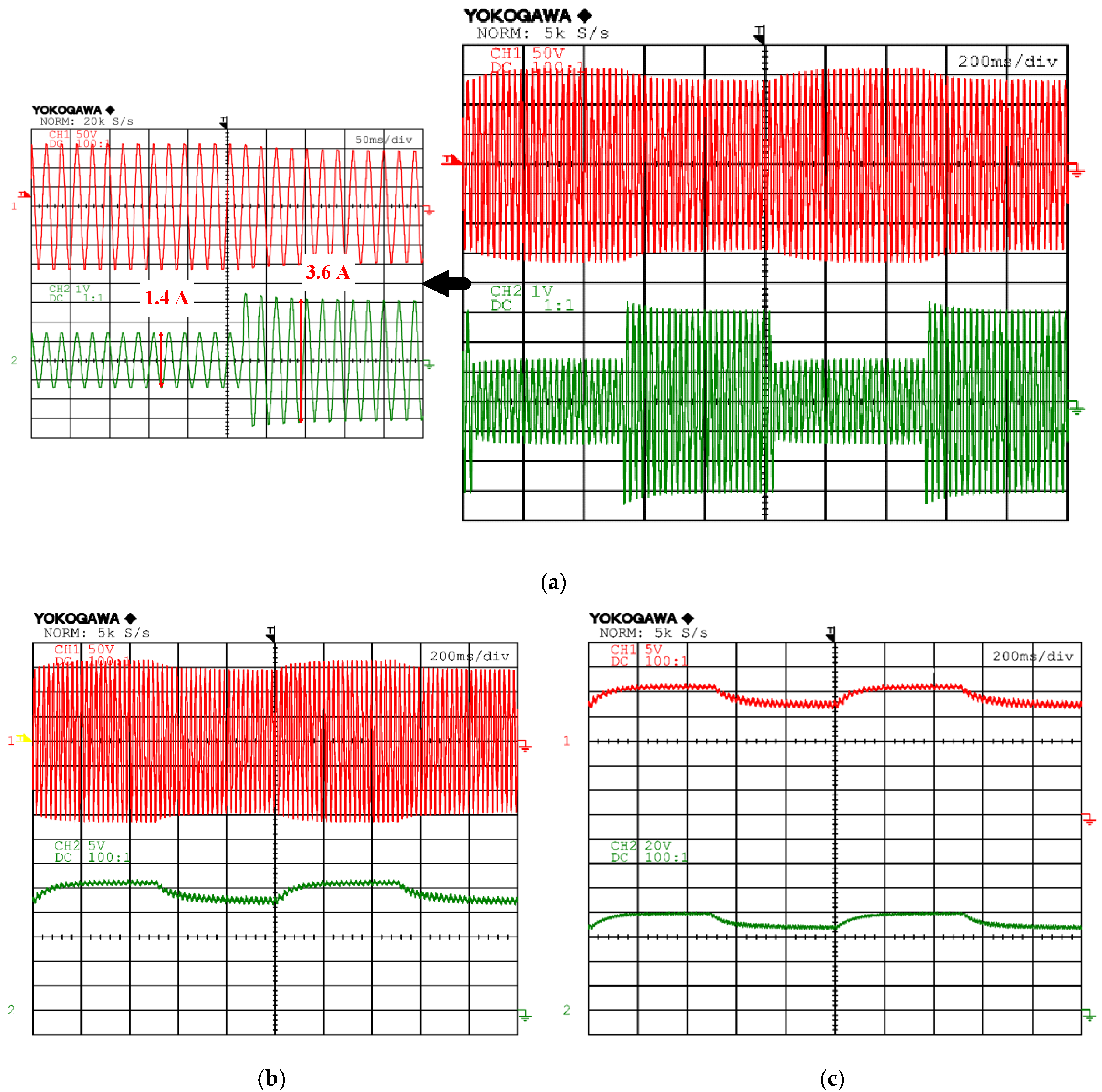
4. Performance Evaluation
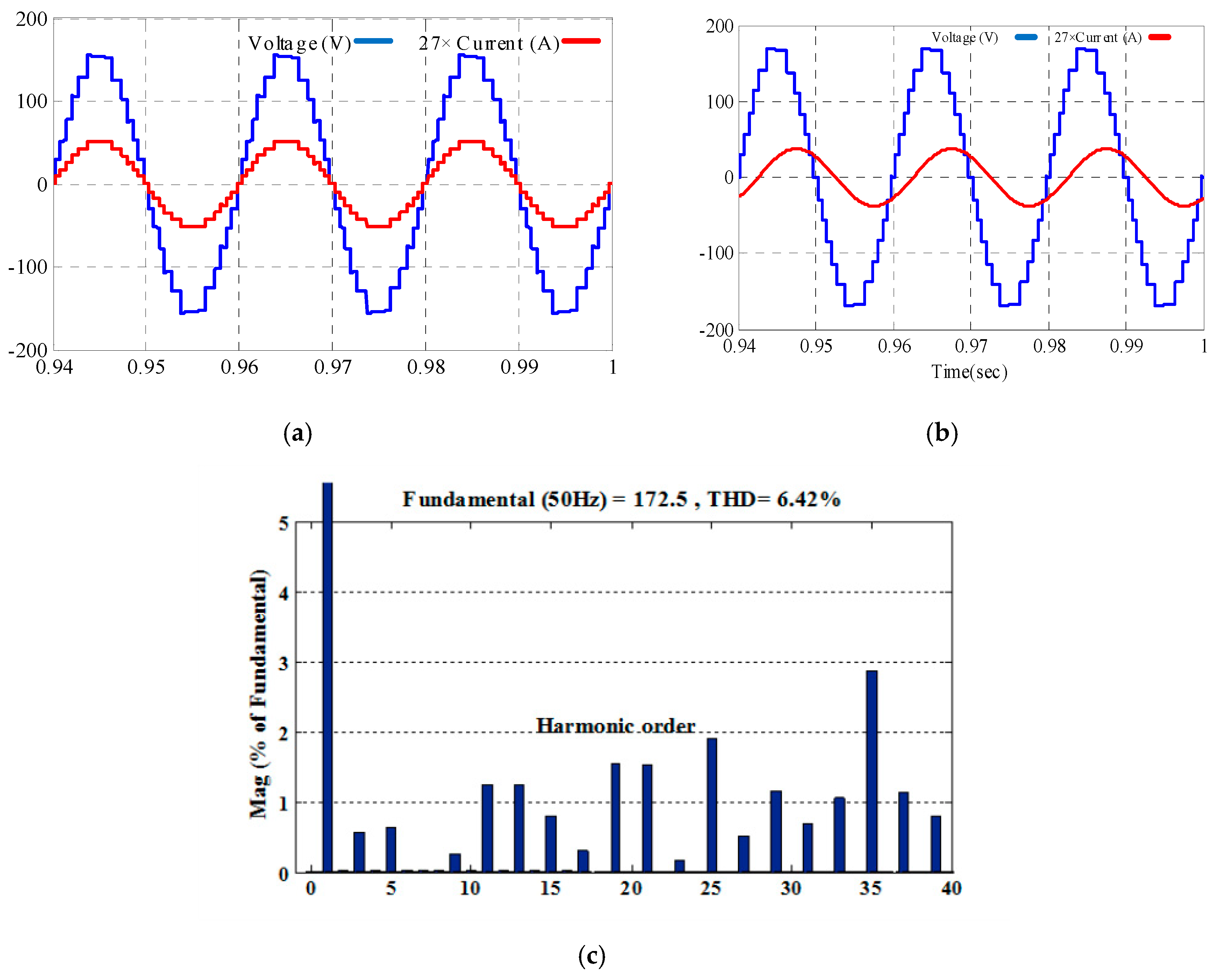
4.1. Simulation Results
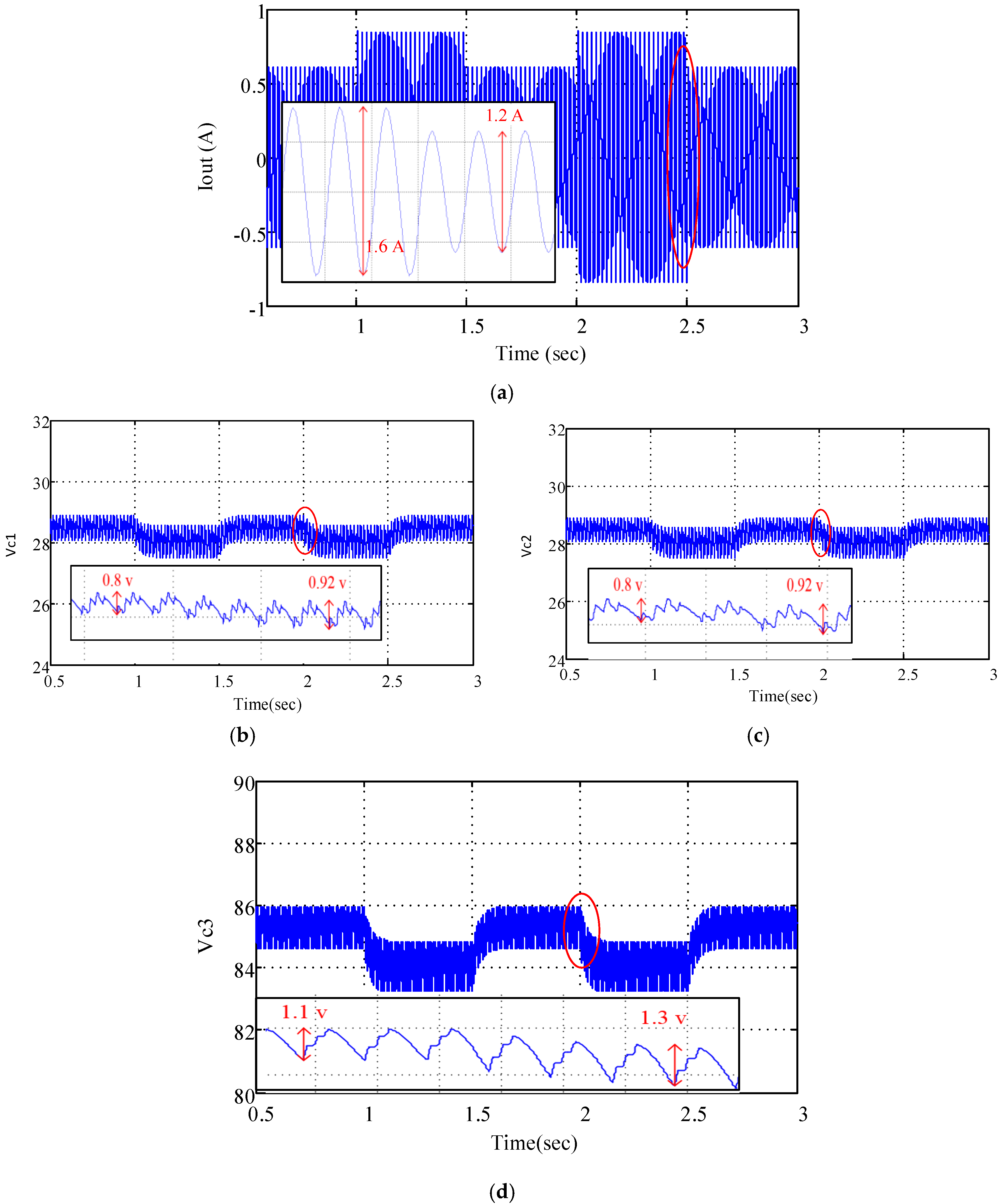
4.2. Experimental Results
5. Conclusions
Author Contributions
Funding
Conflicts of Interest
References
- Franquelo, L.G.; Rodriguez, J.; Leon, J.I.; Kouro, S.; Portillo, R.; Prats, M.A. The age of multilevel converters arrives. IEEE Ind. Electron. Mag. 2008, 2, 28–39. [Google Scholar] [CrossRef]
- Khodaparast, A.; Adabi, J.; Rezanejad, M. A step-up switched-capacitor multilevel inverter based on 5-level T-type modules. IET Power Electron. 2018, 12, 483–491. [Google Scholar] [CrossRef]
- Gupta, K.K.; Ranjan, A.; Bhatnagar, P.; Sahu, L.K.; Jain, S. Multilevel inverter topologies with reduced device count: A review. IEEE Trans. Power Electron. 2016, 31, 135–151. [Google Scholar] [CrossRef]
- Chakraborty, C.; Iu, H.H.C.; Lu, D.D.C. Power converters, control, and energy management for distributed generation. IEEE Trans. Ind. Electron. 2015, 62, 4466–4470. [Google Scholar] [CrossRef]
- Barzegarkhoo, R.; Kojabadi, H.M.; Zamiry, E.; Vosoughi, N.; Chang, L. Generalized structure for a single phase switched-capacitor multilevel inverter using a new multiple DC link producer with reduced number of switches. IEEE Trans. Power Electron. 2016, 31, 5604–5617. [Google Scholar] [CrossRef]
- Chattopadhyay, S.K.; Chakraborty, C. Performance of three-phase asymmetric cascaded bridge (16:4:1) multilevel inverter. IEEE Trans. Ind. Electron. 2015, 62, 5983–5992. [Google Scholar] [CrossRef]
- Barzegarkhoo, R.; Moradzadeh, M.; Zamiri, E.; Kojabadi, H.M.; Blaabjerg, F. A new boost switched-capacitor multilevel converter with reduced circuit devices. IEEE Trans. Power Electron. 2018, 33, 6738–6754. [Google Scholar] [CrossRef]
- Jang, M.; Ciobotaru, M.; Agelidis, V.G. A single-phase grid-connected fuel cell system based on a boost-inverter. IEEE Trans. Power Electron. 2013, 28, 279–288. [Google Scholar] [CrossRef]
- Tseng, K.C.; Huang, C.C.; Shih, W.Y. A high step-up converter with a voltage multiplier module for a photovoltaic system. IEEE Trans. Power Electron. 2013, 28, 3047–3057. [Google Scholar] [CrossRef]
- Du, Z.; Ozpineci, B.; Tolbert, L.M.; Chiasson, J.N. DC–AC cascaded H-bridge multilevel boost inverter with no inductors for electric/hybrid electric vehicle applications. IEEE Trans. Ind. Appl. 2009, 45, 963–970. [Google Scholar] [CrossRef]
- Islam, M.R.; Guo, Y.; Zhu, J. A multilevel medium-voltage inverter for step-up-transformer-less grid connection of photovoltaic power plants. IEEE J. Photovolt. 2014, 4, 881–889. [Google Scholar] [CrossRef]
- Kouro, S.; Malinowski, M.; Gopakumar, K.; Pou, J.; Franquelo, L.G.; Wu, B.; Leon, J.I. Recent advances and industrial applications of multilevel converters. IEEE Trans. Ind. Electron. 2010, 57, 2553–2580. [Google Scholar] [CrossRef]
- Huang, J.; Corzine, K.A. Extended operation of flying capacitor multilevel inverters. IEEE Trans. Power Electron. 2006, 21, 140–147. [Google Scholar] [CrossRef]
- Malinowski, M.; Gopakumar, K.; Rodriguez, J.; Perez, M.A. A survey on cascaded multilevel inverters. IEEE Trans. Ind. Electron. 2010, 57, 2197–2206. [Google Scholar] [CrossRef]
- Ye, Y.; Cheng, K.W.E.; Liu, J.; Ding, K. A step-up switched-capacitor multilevel inverter with self-voltage balancing. IEEE Trans. Ind. Electron. 2014, 61, 6672–6680. [Google Scholar] [CrossRef]
- Peng, W.; Ni, Q.; Qiu, X.; Ye, Y. Seven-level inverter with self-balanced switched-capacitor and its cascaded extension. IEEE Trans. Power Electron. 2019, 34, 11889–11896. [Google Scholar] [CrossRef]
- Lee, S.S.; Bak, Y.; Kim, S.M.; Joseph, A.; Lee, K.B. New Family of Boost Switched-Capacitor Seven-Level Inverters (BSC7LI). IEEE Trans. Power Electron. 2019, 34, 10471–10479. [Google Scholar] [CrossRef]
- Taghvaie, A.; Adabi, J.; Rezanejad, M. A self-balanced step-up multilevel inverter based on switched-capacitor structure. IEEE Trans. Power Electron. 2018, 33, 199–209. [Google Scholar] [CrossRef]
- Khodaparast, A.; Azimi, E.; Azimi, A.; Adabi, M.E.; Adabi, J.; Pouresmaeil, E. A New Modular Multilevel Inverter Based on Step-Up Switched-Capacitor Modules. Energies 2019, 12, 524. [Google Scholar] [CrossRef]
- Hinago, Y.; Koizumi, H. A switched-capacitor inverter using series/parallel conversion with inductive load. IEEE Trans. Ind. Electron. 2012, 59, 878–887. [Google Scholar] [CrossRef]
- Saeedian, M.; Adabi, M.E.; Hosseini, S.M.; Adabi, J.; Pouresmaeil, E. A Novel Step-Up Single Source Multilevel Inverter: Topology, Operating Principle, and Modulation. IEEE Trans. Power Electron. 2018, 34, 3269–3282. [Google Scholar] [CrossRef]
- Taghvaie, A.; Adabi, J.; Rezanejad, M. Circuit topology and operation of a step-up multilevel inverter with a single DC source. IEEE Trans. Ind. Electron. 2016, 63, 6643–6652. [Google Scholar] [CrossRef]
- Liu, J.; Cheng, K.W.E.; Ye, Y. A cascaded multilevel inverter based on switched-capacitor for high-frequency AC power distribution system. IEEE Trans. Power Electron. 2014, 29, 4219–4230. [Google Scholar] [CrossRef]
- Saeedian, M.; Hosseini, S.M.; Adabi, J. A five-level step-up module for multilevel inverters: Topology, Modulation Strategy, and Implementation. IEEE J. Emerg. Sel. Top. Power Electron. 2018, 6, 2215–2226. [Google Scholar] [CrossRef]
- Ioinovici, A. Power Electronics and Energy Conversion Systems: Fundamentals and Hard-Switching Converters; John Wiley & Sons: Hoboken, NJ, USA, 2013; Volume 1. [Google Scholar]
- Saeedian, M.; Hosseini, S.M.; Adabi, J. Step-up switched-capacitor module for cascaded MLI topologies. IET Power Electron. 2018, 11, 1286–1296. [Google Scholar] [CrossRef]
- Sadigh, A.K.; Dargahi, V.; Corzine, K.A. Analytical determination of conduction and switching power losses in flying-capacitor-based active neutral-point-clamped multilevel converter. IEEE Trans. Power Electron. 2016, 31, 5473–5494. [Google Scholar] [CrossRef]


| State | Active Switches | Output Voltage | C1 | C2 | C3 |
|---|---|---|---|---|---|
| 1 | S1,S4,S5,S9,S10,S11,S14 | +6Vdc | ▼ | ▼ | ▼ |
| 2 | S1,S3,S4,S7,S9,S10,S11,S14 | +5Vdc | ▼ | ▲ | ▼ |
| 3 | S1,S3,S5,S6,S9,S10,S11,S14 | +5Vdc | ▲ | ▼ | ▼ |
| 4 | S1,S6,S7,S9,S10,S11,S14 | +4Vdc | - | - | ▼ |
| 5 | S1,S4,S5,S8,S9,S11,S12,S14 | +3Vdc | ▼ | ▼ | ▲ |
| 6 | S1,S3,S4,S7,S9,S12,S14 | +2Vdc | ▼ | ▲ | - |
| 7 | S1,S3,S5,S6,S9,S12,S14 | +2Vdc | ▲ | ▼ | - |
| 8 | S1,S6,S7,S9,S12 | +1Vdc | - | - | - |
| 9 | S1,S4,S5,S8,S9,S11,S12,S13 | 0 | ▼ | ▼ | ▲ |
| 10 | S2,S4,S5,S8,S9,S11,S12,S14 | 0 | ▼ | ▼ | ▲ |
| 11 | S2,S6,S7,S8,S11,S13 | −1Vdc | - | - | - |
| 12 | S2,S3,S5,S6,S8,S11,S13 | −2Vdc | ▲ | ▼ | - |
| 13 | S2,S3,S4,S7,S8,S11,S13 | −2Vdc | ▼ | ▲ | - |
| 14 | S2,S4,S5,S8,S9,S11,S12,S13 | −3Vdc | ▼ | ▼ | ▲ |
| 15 | S2,S6,S7,S8,S10,S12,S13 | −4Vdc | - | - | ▼ |
| 16 | S2,S3,S5,S6,S8,S10,S12,S13 | −5Vdc | ▲ | - | - |
| 17 | S2,S3,S4,S8,S10,S12,S13 | −5Vdc | ▼ | ▲ | ▼ |
| 18 | S2,S4,S5,S8,S10,S12,S13 | −6Vdc | ▼ | ▼ | ▼ |
| Output Voltage Level | Equivalent Parasitic Resistance |
|---|---|
| 0 | 6Ronsw + 1RonD |
| ±1Vin | 3Ronsw + 3RonD |
| ±2Vin | 4Ronsw + 3RonD |
| ±3Vin | 6Ronsw + 2RonD |
| ±4Vin | 5Ronsw + 2RonD |
| ±5Vin | 6Ronsw + 2RonD |
| ±6Vin | 7Ronsw |
| Items | [21] | [16] | [27] | [6] | [19] | X-Type |
|---|---|---|---|---|---|---|
| No. of Capacitors | ||||||
| No. of Switches | ||||||
| No. of Drivers | ||||||
| No. of Series Diodes | 0 | 0 | 0 | 0 | ||
| PIV(×VIN) | ||||||
| TSV(×VIN) | ||||||
| Polarity Generating | H-bridge | H-bridge | H-bridge | H-bridge | inherent | inherent |
| Bi-Directional Power Flow | NO | NO | YES | NO | NO | YES |
| Parameters | Values |
|---|---|
| Input DC Source (Vin) | 30 V |
| Boost Ratio (n) | 6 |
| Output frequency (fo) | 50 Hz |
| Capacitances (C) | C1 = C2 = 4700 µF, C3 = 2200 µF |
| Load (ZL) | 90 Ω, 318 mH |
| Parameters | Values |
|---|---|
| Input DC voltage (Vin) | 30 V |
| Boost Ratio (n) | 6 |
| Output Frequency (fo) | 50 Hz |
| Capacitances (C) | C1 = C2 = 4700 µF, C3 = 2200 µF |
| Load (ZL) | 90 Ω, 318 mH |
| Main Switches (MOSFET) | IRFP460 |
| Opto-coupler Driver | HCPL-3120 |
| Main Control Chip | AVR ATMEGA16A |
| Voltage Probe | PINTEK DP-50 |
| Current Probe | FLUKE 80i-110s AC/DC |
Publisher’s Note: MDPI stays neutral with regard to jurisdictional claims in published maps and institutional affiliations. |
© 2020 by the authors. Licensee MDPI, Basel, Switzerland. This article is an open access article distributed under the terms and conditions of the Creative Commons Attribution (CC BY) license (http://creativecommons.org/licenses/by/4.0/).
Share and Cite
Azimi, E.; Khodaparast, A.; Rostami, M.J.; Adabi, J.; Adabi, M.E.; Rezanejad, M.; M. G. Rodrigues, E.; Pouresmaeil, E. X-Type Step-Up Multi-Level Inverter with Reduced Component Count Based on Switched-Capacitor Concept. Electronics 2020, 9, 1987. https://doi.org/10.3390/electronics9121987
Azimi E, Khodaparast A, Rostami MJ, Adabi J, Adabi ME, Rezanejad M, M. G. Rodrigues E, Pouresmaeil E. X-Type Step-Up Multi-Level Inverter with Reduced Component Count Based on Switched-Capacitor Concept. Electronics. 2020; 9(12):1987. https://doi.org/10.3390/electronics9121987
Chicago/Turabian StyleAzimi, Erfan, Aryorad Khodaparast, Mohammad Javad Rostami, Jafar Adabi, M. Ebrahim Adabi, Mohammad Rezanejad, Eduardo M. G. Rodrigues, and Edris Pouresmaeil. 2020. "X-Type Step-Up Multi-Level Inverter with Reduced Component Count Based on Switched-Capacitor Concept" Electronics 9, no. 12: 1987. https://doi.org/10.3390/electronics9121987
APA StyleAzimi, E., Khodaparast, A., Rostami, M. J., Adabi, J., Adabi, M. E., Rezanejad, M., M. G. Rodrigues, E., & Pouresmaeil, E. (2020). X-Type Step-Up Multi-Level Inverter with Reduced Component Count Based on Switched-Capacitor Concept. Electronics, 9(12), 1987. https://doi.org/10.3390/electronics9121987