Article

Comparative Performance and Assessment Study of a Current-Fed DC-DC Resonant Converter Combining Si, SiC, and GaN-Based Power Semiconductor Devices

by
Oscar Miguel Rodríguez-Benítez
1,
Mario Ponce-Silva
1,*,
Juan Antonio Aquí-Tapia
2,
Abraham Claudio-Sánchez
1,
Luis Gerardo Vela-Váldes
1,
Ricardo Eliu Lozoya-Ponce
3 and
Claudia Cortés-García
1
1
Department of Electronics Engineering, National Technology of Mexico—CENIDET, Morelos 62490, Mexico
2
Research and Development Department, OSRAM, Monterrey 66600, Mexico
3
Graduate Studies and Research Division, National Technology of Mexico—IT Chihuahua, Chihuahua 31310, Mexico
*
Author to whom correspondence should be addressed.
Electronics 2020, 9(11), 1982; https://doi.org/10.3390/electronics9111982
Submission received: 2 November 2020 / Revised: 18 November 2020 / Accepted: 18 November 2020 / Published: 23 November 2020
(This article belongs to the Special Issue Innovative Technologies in Power Converters)

Abstract

:
This paper focuses on the main reasons of low efficiency in a current-fed DC-DC resonant converter applied to photovoltaic (PV) isolated systems, comparing the effects derived by the overlapping time in the gate-signals (gate-source voltage) combining silicon (Si), silicon carbide (SiC), and gallium nitride (GaN)-based power devices. The results show that unidirectional switches (metal–oxide–semiconductor field-effect transistors (MOSFETs) plus diode) present hard switching as a result of the diode preventing the MOSFET capacitance of being discharged. The effectiveness of the converter was verified with a 200-W prototype with an input voltage range of 0–30.3 V, an output voltage of 200 V, and a switching frequency of 200 kHz. The reduction losses by applying GaN versus Si and SiC technologies are 66.49% and 53.57%, respectively. Alternatively, by applying SiC versus Si devices the reduction loss is 27.84%. Finally, according to the results, 60% of losses were caused by the diodes on both switches.

1. Introduction

Photovoltaic (PV) energy has received a great attention in research and industry because it is one of the most efficient and effective solutions to the environmentally friendly sources [1]. It can be classified into isolated systems and interconnected systems. Isolated systems represent those applications that store energy in battery banks, and the interconnected systems supply the generated energy by the PV panel to the electrical grid, satisfying standards as appropriate.
The interconnected systems represent one of the most studied applications, generally, they are represented by five stages. The first stage allows a low-frequency ripple. The second stage increases the voltage level from the PV according to the inverter specifications. The third and fourth stages represent the decoupling capacitor and the inverter, which has to fulfill three functions: 1. to shape the current into a sinusoidal waveform, 2. to invert the current into an AC current, and 3. if the PV array voltage is lower than the grid voltage, the PV array voltage must be boosted with an additional element. This last point is important because there must be no reverse energy to the DC source. Finally, the fifth stage filters the sinusoidal signal.
Alternatively, the PV energy varies with changes in atmospheric conditions and the non-linear source. According to the literature, there are control schemes to deliver the maximum power considering changes in atmospheric conditions, load demands, or external faults. Examples of common control schemes in the Maximum Power Point Tracking (MPPT) are presented in [1,2,3,4]. Furthermore, there are some studies that evaluate the MPPT control by applying current controllers as proportional integral (PI), hysteresis, predictive, and sliding-mode controllers [5] maintaining the stable operation of a grid-connected PV system as they can regulate the current to follow the reference current (PV system).
In this way, it is necessary to take into account a controller through partial feedback linearization, and a calculation of the sinusoidal reference current in order to control the current injected into grid, thus the operation of the PV system at the MPPT is guaranteed [6].
One of the key energy conversion systems of the PV-interconnected systems is the DC-DC power converter (stage two), which can be divided into two categories: resonant and non-resonant converters. The non-resonant converters represent the most studied topologies for PV-interconnected systems. One of the widely used is the Boost converter [7,8,9]. Part of the problem using a Boost converter is related to the need to use two large inductors, causing a challenging point on the size reduction [10]. Furthermore, due to its limited efficiency, it is generally a viable option for low power applications.
Similar to the Boost converter, the conventional [11,12,13,14] and active [15,16] Flyback converters are typically used, showing some disadvantages related to the high percentage of energy managed by the transformer, considerably increasing its size. In addition, the “stress” presented by the rectifier diode and the issue of pulsating input current make it a system that requires the placement of additional capacitive elements.
Recently, several DC-DC resonant converters have been reported in the literature since they present a higher efficiency working at higher frequencies and higher power density than the conventional DC-DC converters. These resonant converters could be divided into two categories: voltage-fed DC-DC resonant converters (VFRC) and current-fed DC-DC resonant converters (CFRC).
The VFRC represent the majority of the resonant topologies applied [17,18,19,20,21,22,23,24,25] and have less components, higher efficiency, higher power density, and frequency operation. However, these topologies present a pulsating input current, thereby, it is necessary to use an additional filter stage [26].
On the other hand, the CFRC represent the minority of the studied topologies in PV-interconnected systems [27,28,29,30] and do not present a pulsating input current, and thus the stage to avoid the ripple current being reflected to the PV system is unnecessary. However, the main disadvantages of these topologies are the requirements of a large inductor to feed the inverter with current instead of voltage, as well as the use of unidirectional switches. This point results in one of the primary reasons of low efficiency in the whole converter. Additionally, the control stage is more complex.
The use of CFRC is based on parallel resonant tanks, and the unidirectional switches used can be applied by IGBTs, BJTs or an array of a metal–oxide–semiconductor field-effect transistor (MOSFET) in series with a diode. These converters usually present zero voltage switching (ZVS), and in comparison with other resonant converters, they commonly use only two choke inductors instead of the push-pull current source inverter (CSI), and only two grounded switches instead of the full-bridge. Moreover, the CFRC satisfy the front-end DC-DC converter requirements for this application since the two current-fed inductors used comprise a high gain voltage ratio. Additionally, in comparison with topologies fed in voltage, the CFRC has independent active/reactive power control and fast dynamic response [31].
According to the last characteristics, there is a need to study the feasibility of the minority part of topologies applied in PV-interconnected systems. In this sense, the main contribution of this paper is to assess the performance of the CFRC applied in PV-isolated systems (in stage 2), specifically considering the losses in the unidirectional switches comparing the key performance indicators for silicon (Si), silicon carbide (SiC), and gallium nitride (GaN)-based power devices.
This paper is divided as follows: Section 2 presents the topology, design methodology, study of key parameters in power losses, and a brief comparison of key performance indicators for Si, SiC, and GaN power devices. Section 3 shows the experimental results. Section 4 presents a study of the power losses originating from the commutations and the overlap of the unidirectional switches used. Finally, Section 5 presents the conclusions.

2. Current-Fed DC-DC Resonant Converter and Power Devices

Based on [32], there are different configurations of CFRC. For this work, the studied current inverter is the two current sources resonant inverter. The resonant inductor of the parallel resonant tank is changed by a transformer to obtain galvanic isolation. The sinusoidal signal obtained from the parallel resonant tank is rectified with a full-bridge rectifier and filtered with an LC filter.
An important characteristic in a CFRC is that the current source must be short-circuited. The time in both switches (S1 and S2) during the short-circuit is named overlapping. In this time, the parallel resonant tank is isolated to the rest of the circuit. To obtain this isolating, it is necessary to use unidirectional switches to prevent the flow of AC current to the DC side of the inverter [33]. To establish unidirectional switches, it is possible to use two arrays: the first one by a diode in series with a MOSFET and the second one by an IGBT.
The general characteristics of both arrays have been discussed and compared before [34,35,36]. Basically, the primary disadvantage of IGBT is related to the operational frequency, since it can only operate in frequency ranges of up to 150 kHz. On the other hand, the array configured by a MOSFET in series with a diode partially solves the switching frequency problem. However, the primary problem with this configuration is the increase in parasitic capacitances (MOSFET and diode), which represent a substantial increase in power loss. Therefore, a selection of the semiconductor devices to be used in the experimental stage should be performed.
Considering remarks and because the motivation to use resonant converters is the relation of higher power/weight and power/size ratios, the arrangement to allow operation at a high switching frequency needs to be considered. In this manner, not only the large passive elements need to be considered in the converter design, but also the efficiency target and thermal design. Therefore, Figure 1 shows the CFRC studied.
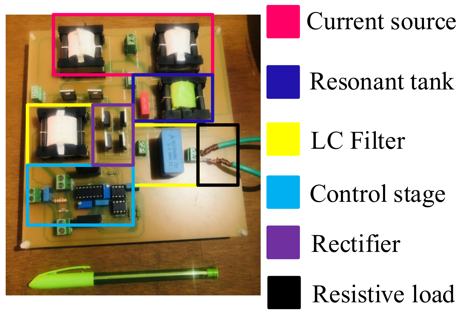
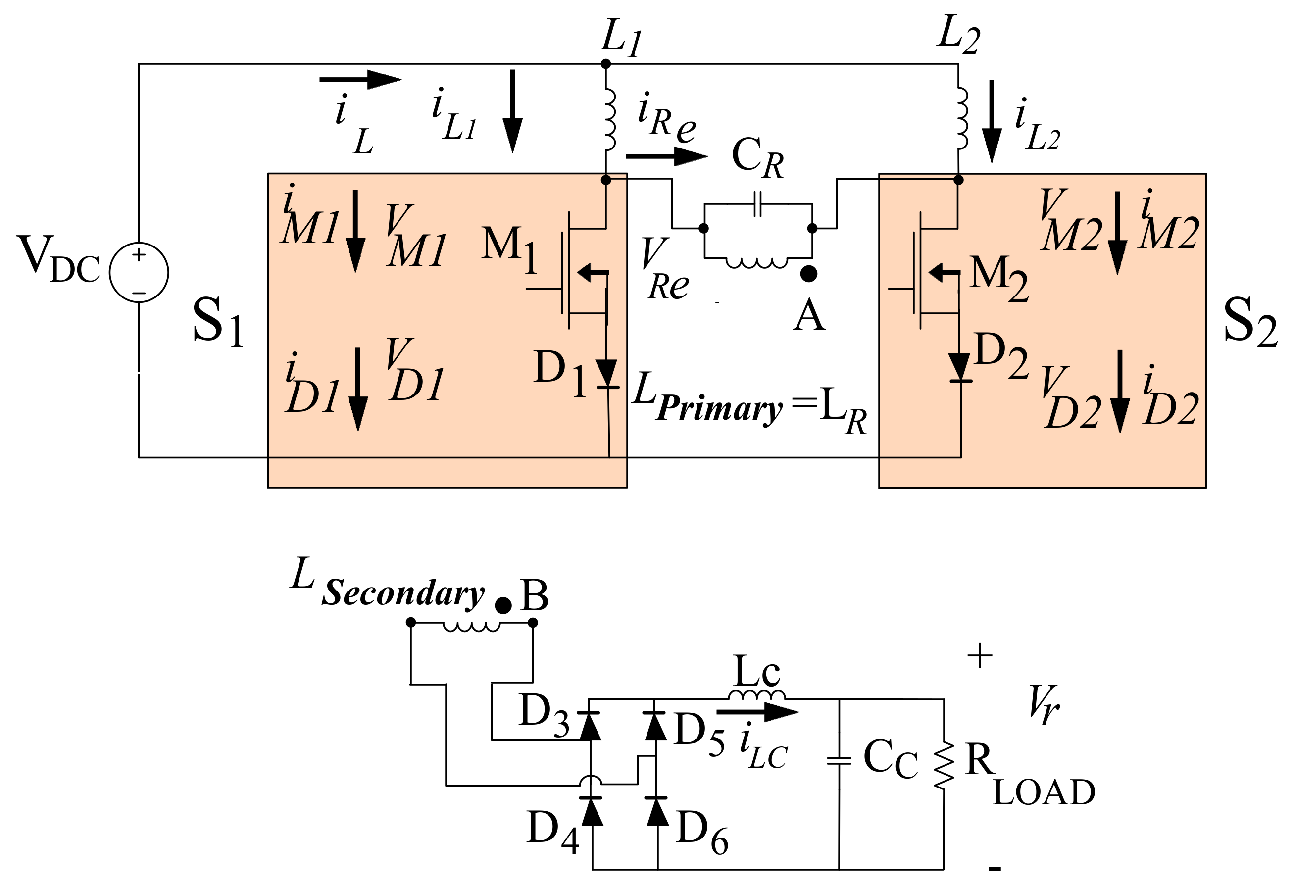
The topology shown in Figure 1 is comprised of four stages: the first stage consists of two current sources (L1 and L2) and a DC voltage source (VDC), the second stage by a parallel resonant tank (LPrimary and CR) with magnetic isolation derived by LPrimary, where LPrimary is coupled to LSecondary (from part A to B), the third stage by a full-wave rectifier (D3D6), and the fourth stage by the decoupling elements (Cc and Lc). The operation of the circuit is as follows: the two inductors L1 and L2 provide the two current sources to the parallel resonant tank, the unidirectional switches S1 and S2 short-circuit the current sources periodically in order to feed the parallel resonant tank formed by the transformer (composed by LPrimary and LSecondary) and the resonant capacitor CR with a square current waveform. The parallel resonant tank filters this waveform and applies a sinusoidal voltage waveform to the full-bridge rectifier (D3, D4, D5 and D6). The rectified signal is filtered by LC and CC and it is applied to the load (RLOAD). One important characteristic of the CFRC (Figure 1) is the need to have an overlapped control, because if there is no overlapping control between M1 and M2, the inductance (L1) would be charged by the current iL1 (t), and the current iL2 (t) from the second inductance (L2) would flow directly through the resonant tank. Under the dual condition, iL1 (t) would flow through the resonant tank and iL2 (t) through L2. However, if there is no overlapped control, iL1 (t) and iL2 (t) could be canceled, although not completely, producing a considerable increase in the losses on the unidirectional switches. Furthermore, the resonant tank and the components used need to be carefully selected, since these parameters directly affect the overlap signals in S1 and S2. Additionally, the high frequency transformer is a critical part of the resonant converter. Its design affects efficiency, weight, and dimension of the whole topology. This fact is important to improve the efficiency of the topology. Considering these statements, a brief comparison of different semiconductor devices should be performed. As a result of the advancement in the field of power semiconductor technologies [37,38,39], SiC MOSFETs, SiC junction gate field-effect transistors (JFETs), SiC Schottky barrier diodes, and gallium nitride (GaN) transistors provide a valuable opportunity to obtain high efficient performance with compact size. Part of the primary characteristics in all power semiconductor devices are related to the operating at high power, high frequency, and high temperature. In fact, many works have been reported in the literature analyzing the physical breakdown mechanisms, modeling, characterizations, and the trade-off characteristics between the breakdown voltage and the on-resistance of Si, SiC, and GaN-based power semiconductor devices [40,41,42,43]. As a result of these studies, some characteristics are shown in Table 1.
The capacity to achieve high switching frequency in every semiconductor is directly proportional to its drag-velocity. The speeds present in GaN devices are more than twice the speed in Si components, achieving commutations at much higher frequencies. However, a negative characteristic by GaN devices in comparison with Si and SiC is less thermal conductivity [44,45,46], which means the heat generation of SiC devices can be easily dissipated as compared to GaN. From the previous characteristics, one of the key behaviors to compare with these power devices in a CFRC is the overlap stage control. In this way, a brief study of this condition is presented below.

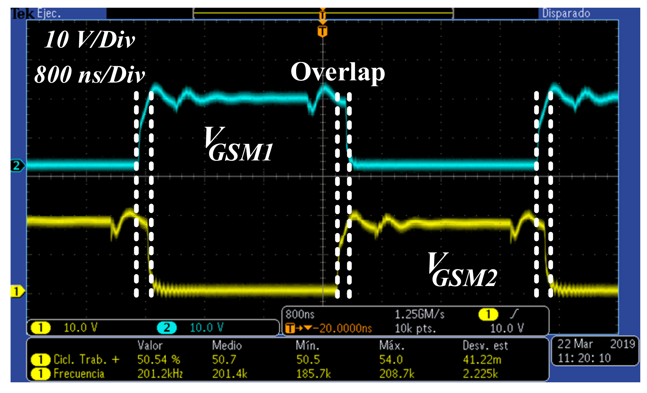
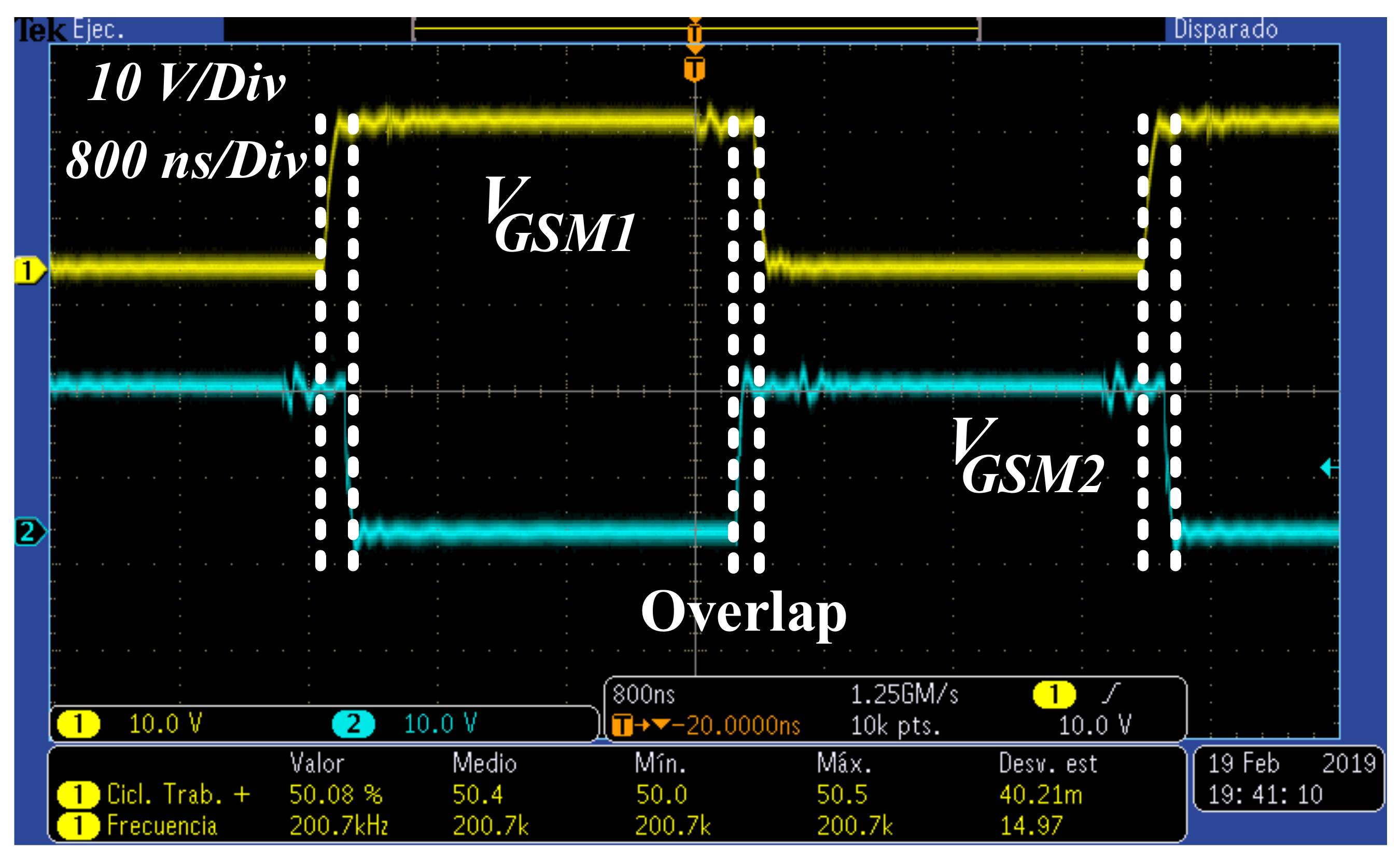
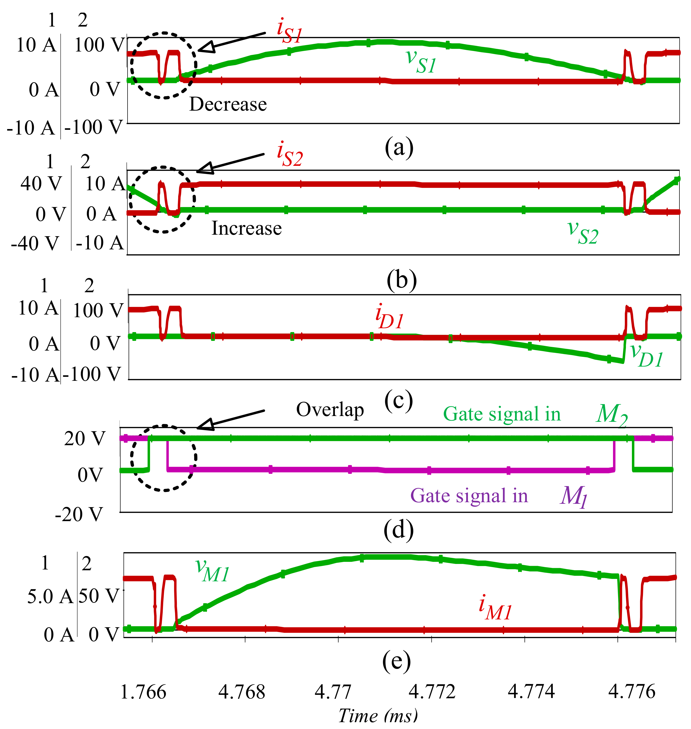
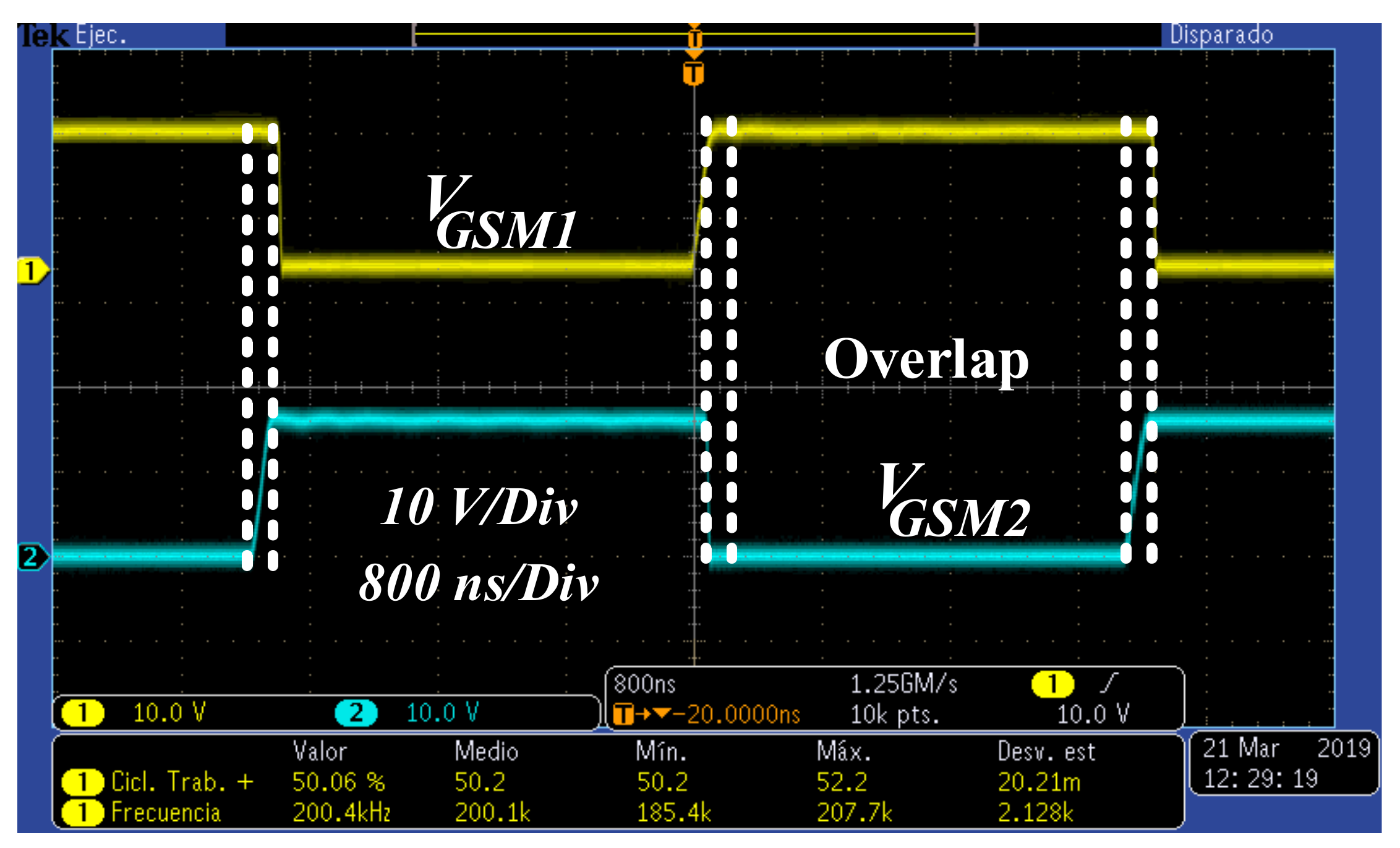
Overlap in Gate-Signals of M1 and M2

To determine the effect of the overlap, an initial simulation study is developed under the following considerations: (1) time delay proposed between the turn on of M1 and M2 is 0.49, this value was taken because TD must be as close as 0.5, with the aim of not having such a long overlap; (2) a quality factor of the resonant tank is sufficiently high to filter all the current harmonics, except the fundamental; (3) all inductors and capacitors are lossless; (4) D3, D4, D5, and D6 are ideal diodes; and (5) unidirectional switches were performed by SiC diodes (C4D08120) and SiC MOSFETs (C2M0160120D), because of their improvements for AC-DC and DC-DC converters. These devices can operate with reduced conduction and switching losses over higher frequencies, and higher temperatures minimize the requirements for the passive components and reduce cooling demands [47,48,49]; however, the performance given by SiC power devices will be compared with Si and GaN. The switching frequency (Fsw) was considered to be 200 kHz. The simulation results in Figure 2 created in PSpice® show the key waveforms of S1 (Figure 2a), S2 (Figure 2b), D1 (Figure 2c), gate-signals in M2 (Figure 2d), and M1 (Figure 2e). These simulation results are also based on the design parameters and design methodology shown in Table 2 and Table 3.
From Figure 2, when the overlap begins (gate-signal in M1 and gate-signal in M2 are in the on-state), the current iS1 decreases to zero, and the current iS2 increases. This behavior is related to the charge and discharge of the internal stray capacitances of D1 and D2.
In this sense, when S2 is in the on-state, M2 can be modeled by its output parasitic capacitance in parallel with its parasitic resistance, and D2 as a parallel made up of the same diode and its stray capacitance. Furthermore, 
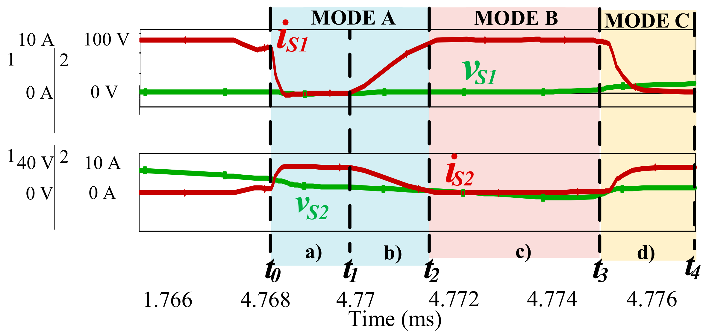
Figure 3 shows the hard switching in D1 and M1 caused by the effect given by the overlap. In this manner, to determine the converter performance effects, based on Figure 3, three modes are proposed considering the current and voltage waveforms of S1 and S2; therefore, the first mode (MODE A from t0 to t2) performs a fall-rise of is1 and a rise-fall of is2, the second mode (MODE B from t2 to t3) represents the time when is1 keeps its value and is2 is zero, and the third mode (MODE C from t3 to t4) represents the dual condition of MODE B.
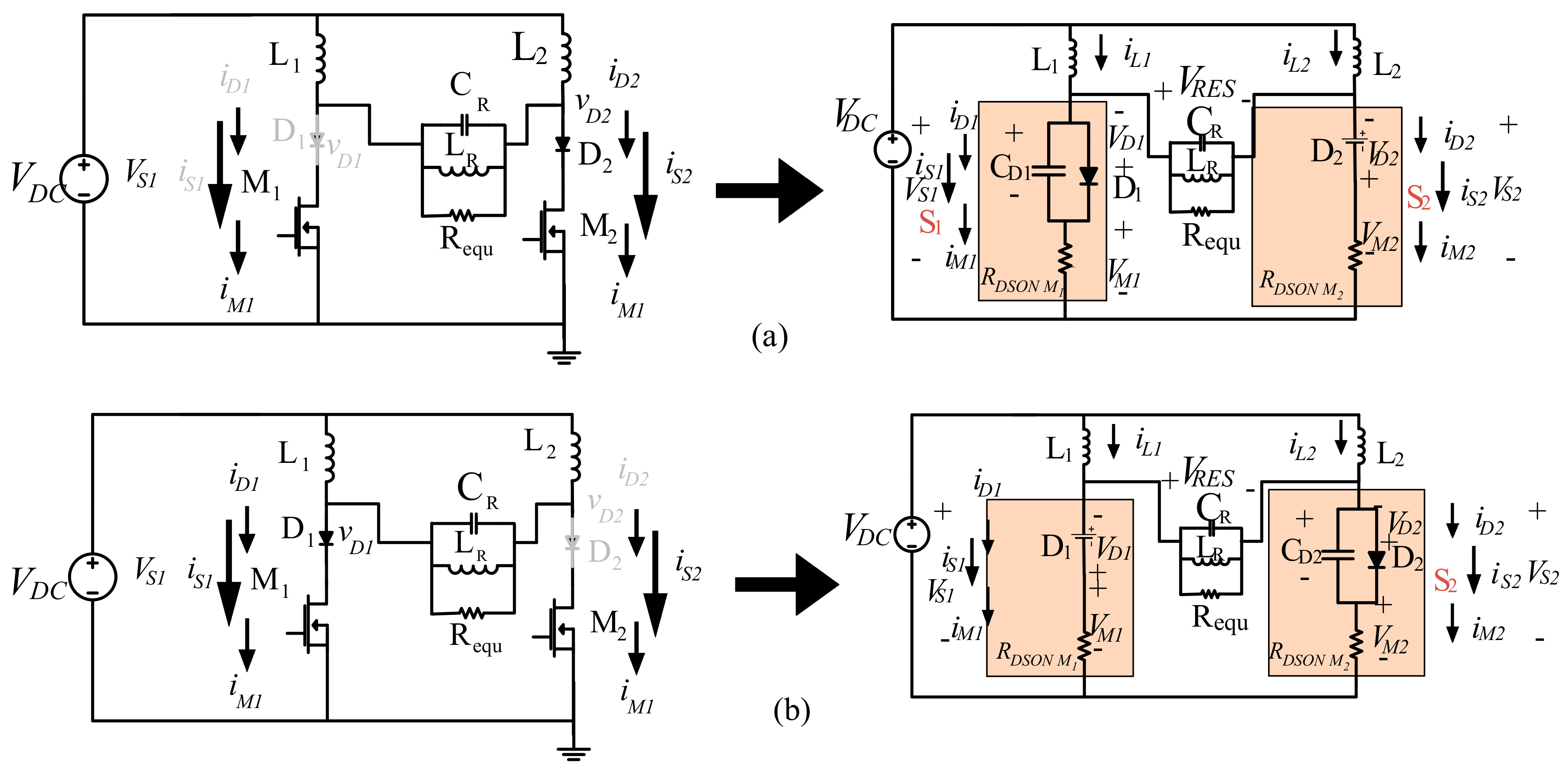
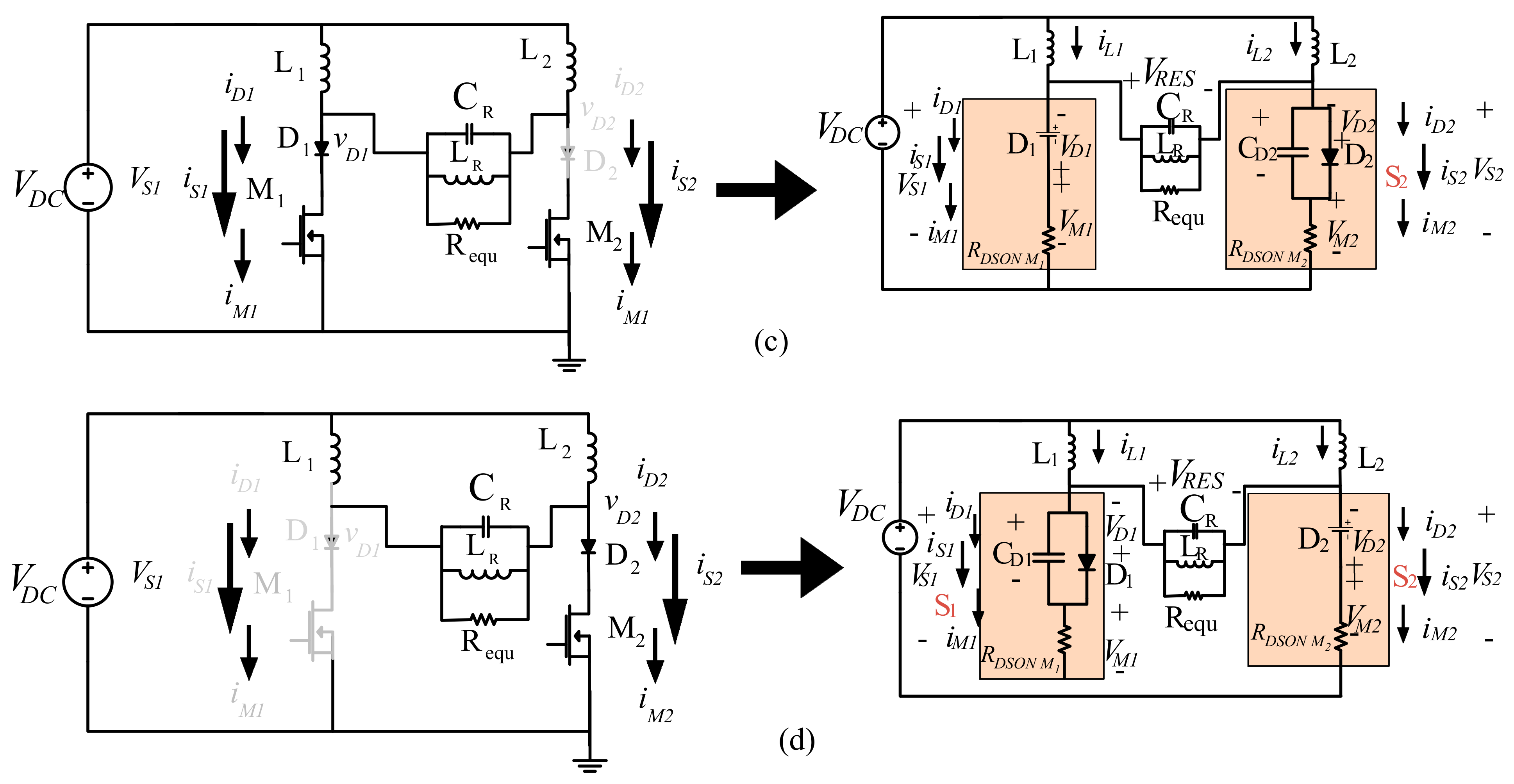
From Figure 3 and based on times t0 to t4, the equivalent circuits are obtained, as shown in Figure 4. In these circuits, an equivalent resistance (Requ) was considered as the load in the resonant tank, where Requ represents the RLOAD seen from Lr. Then, based on the operation, MODES are shown during the overlap and equivalent circuits in Figure 3 and Figure 4, respectively. The modes A, B, and C are detailed below:
Time t0-t1 (Figure 4a): this time starts when the gate-signal in M2 is in the on-state, thereby the overlap starts. During this time, iS1 decreases to zero (and remains at 0 A) and iS2 increases its value the same as the input current (IL). Moreover, since S2 is in the on-state, the diode D1 can be modeled as a parallel by the same diode and its stray capacitance CD1, and M1 by a drain-source resistance RDSON M1. In this moment, the voltage of the stray capacitance in D1 (VCD1) can be represented as shown in Equation (1).
V C D 1 = V R E S V D S M 1 V D S M 2 V D 2
where VRES is the voltage of the resonant tank, VDSM1 represents the voltage drain-source in M1, VDSM2 the voltage drain-source in M2, and VD2 the forward voltage in D2. Furthermore, in this time, there is a “charge” condition in CD1 which generates an increase of switching losses in S1 until the voltage in D1 reaches its forward voltage.
Time t1t2: It represents the instant when iS1 increases and iS2 decreases its value, turning on S1, and modeled D2 as a parallel by D2 and its stray capacitance CD2, and M2 by a drain-source resistance RDSON M2 (Figure 4b). In this time, the voltage of the stray capacitance in D2 (VCD2) can be represented as shown in Equation (2), where VD1 represents the forward voltage in D1.
V C D 2 = V R E S V D S M 1 V D S M 2 V D 1
Time t2t3: In MODE B (Figure 4c), M1 and M2 are in the on-state. Furthermore, is1 stays constant and is2 stays at 0A, modeling D2 and M2 the same as from t1 to t2. On the other hand, there is no current in S2 but there is a voltage in D2, increasing the power losses. Moreover, the voltage of the stray capacitance in D2 (VCD2) can be represented the same as Equation (2).
Time t3t4: MODE C starts (Figure 4d), the gate-signal in M1 is in the off-state, and thus the overlap is finished. Furthermore, M2 is in the on-state and is2 is increasing. During this time, S1 is in the off-state after finishing the discharging process, which causes the stored energy to be lost not only in M2 but also in D2. Additionally, as a result of M1 in the off-state, VRES will be split in D1 and M1 with a complementary voltage in D2. In fact, VCD2 can be modeled as shown in Equation (3).
V C D 2 = V R E S V D S M 1 V D S M 2
From Figure 3 and Figure 4, the behavior given by the recovery time in D1 and D2 during their shutdown states causes D1 and D2 to be in the on-state even when M1 and M2 are in the off-state, which indicates that if the complete switch is analyzed, the MOSFET and diode do not share the same shutdown time. Furthermore, in MODE A, iS2 increases, and the stray capacitance in D1 is discharging, causing iS1 to decrease to zero, then, the current iS1 increases its value because the current iS2 decreases. This current will be zero, until the voltage in D2 is zero again.
In this sense, when the voltage in D2 is zero, the current iS2 will increase, therefore, this is the main reason to generate hard switching in the complete switch. On the other hand, the power losses achieved in the simulation by S1 plus S2 are 31 W with a global efficiency of 62% and a time delay between gate-signals of 0.49. It is important to estimate the applied overlap. Therefore, 
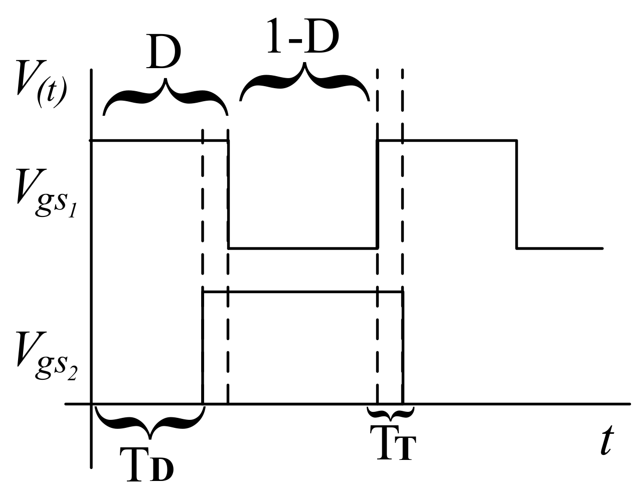
Figure 5 shows the overlap to consider in the analysis.
From Figure 5, D is the applied duty cycle, the time delay between the gate-signals of M1 and M2 (VGSM1 and VGSM2), and represents the overlap time when M1 and M2 are in the on-state. As mentioned, TT is defined in Equation (4) and TD is defined in Equation (5).
T T = D 1 D
T D = D T T
Replacing (4) into (5) and considering that the energy transferred to the load depends on the duty cycle, the selected duty cycle of the resonant tank is 0.5.
T D = 2 D 2 D + 1 2
T D = 1 2
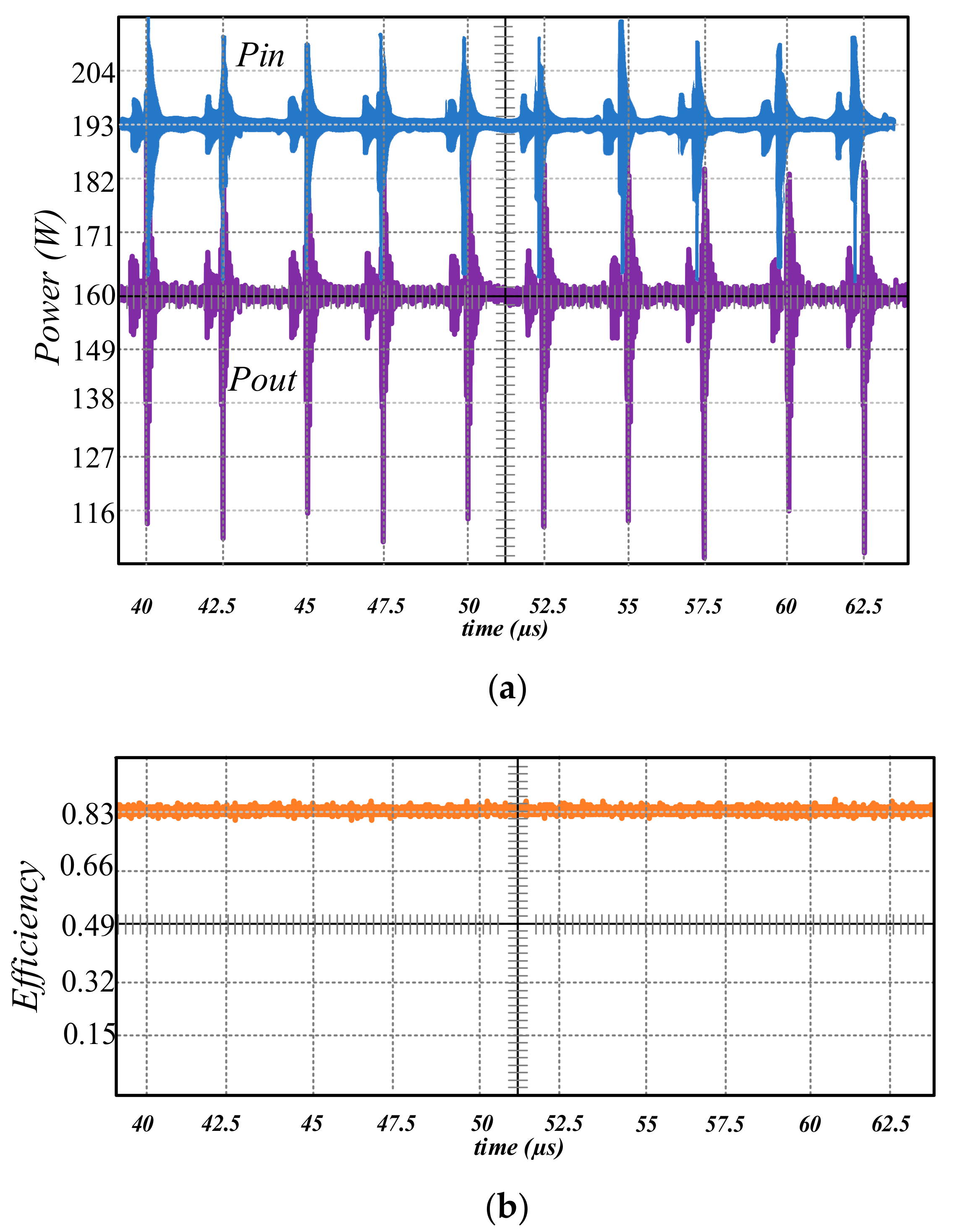
To assess the combination of power semiconductor devices in the unidirectional switch and to verify Equation (7) based on the parameters and design methodology described above, three different converters are designed combining Si-MOSFET and diode (first array), SiC-MOFET and diode (second array), and GaN-transistor SiC-diode (third array). The power devices are selected based on the stress level calculations as well as the similarity in the electrical ratings between the Si and SiC devices (as a result of the reduced drain to source voltage in the GaN-transistor), parasitic capacitances, current rating, switching speed, on-resistance, maximum junction temperature, and following the primary comparison between the characteristics of every device [50,51], mainly focused in the work presented in [52]. Therefore, Table 4 shows the specifications of each power device used in the design.
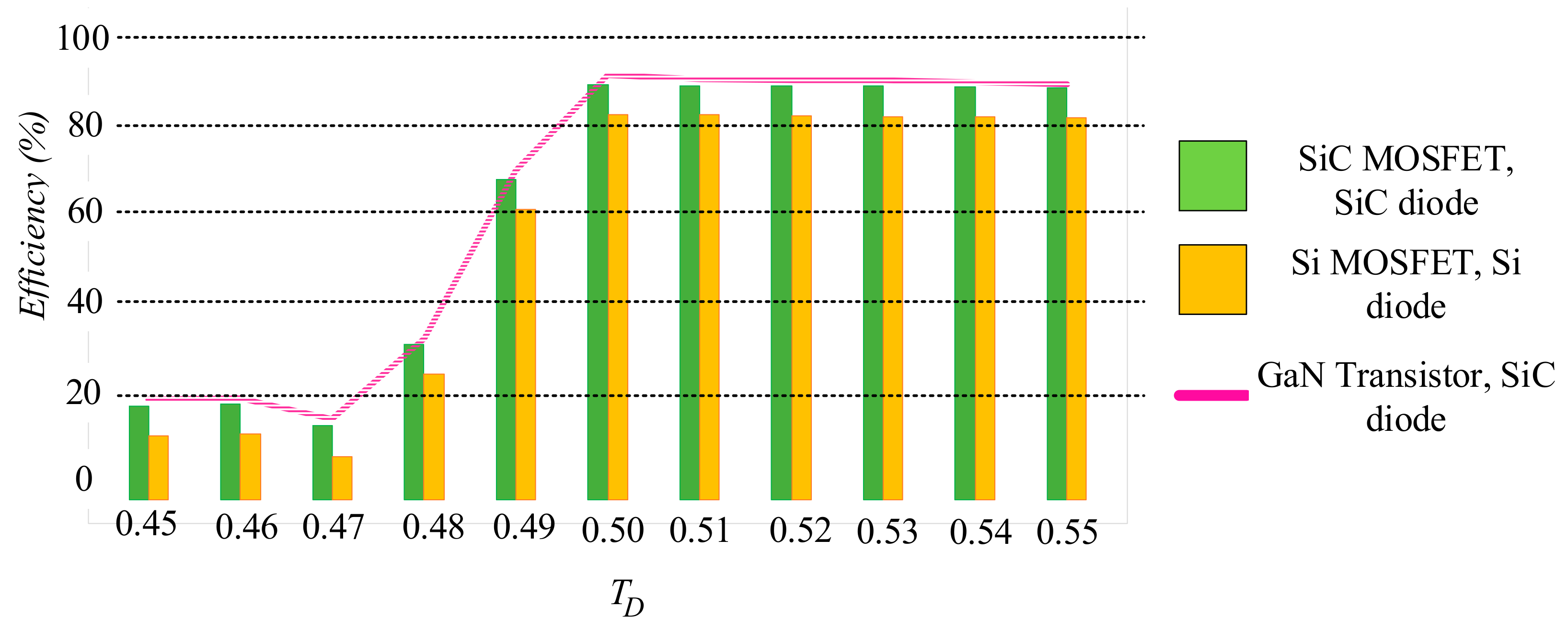
Figure 6 shows the efficiency versus variations in TD performed by different power semiconductor devices obtained in the simulation.
According to Figure 6 and considering TD = 0.5, a global efficiency and total power losses (switching plus conduction) in S1 plus S2 of 86% and 27 W were performed by the Si-MOSFET and Si-diode combination. Furthermore, SiC-MOSFET plus SiC-diode performed an efficiency and power losses in S1 plus S2 of 92.7% and 14 W, respectively. Finally, the performance given by the combination of GaN-transistor plus SiC-diode were similar to the combination of SiC-MOSFET plus SiC-diode with an efficiency of 94% and power losses in S1 plus S2 of 11 W.
Moreover, the performance given by the overlap dramatically affects the efficiency of the whole converter, thus, it is suggested to take into account an overlapped control in a CFRC since the problems associated with the discharging of the transistor output the capacitance (Cout). When the switch voltage increases, the MOSFET (M1) Cout is charged via D1 to the peak value of the switch voltage, and then remains at that voltage until the transistor turns on. At this time, the capacitance Cout is discharged through the transistor, resulting in switching loss. According to Figure 6, with TD estimated to be 0.5, the power losses in S1 plus S2 and global efficiency performed by SiC-MOSFET plus SiC-diode were 14 W and 92.7 %, which performance is reasonably similar in comparison with the combination of GaN-transistor plus SiC-diode. In this way, the complete simulation results achieved from the DC-DC resonant converter performed by SiC-MOSFET plus SiC-diode are presented in
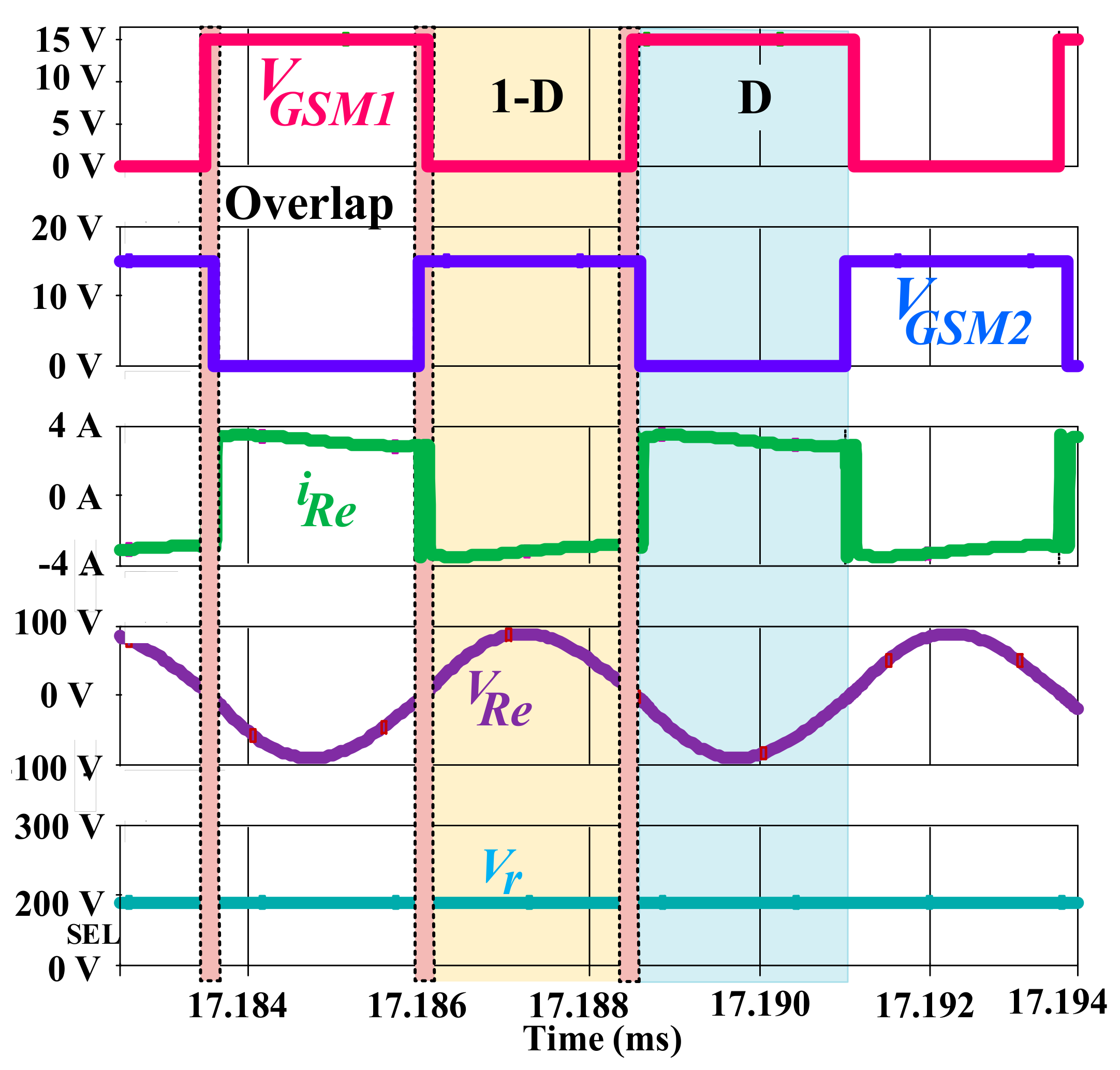
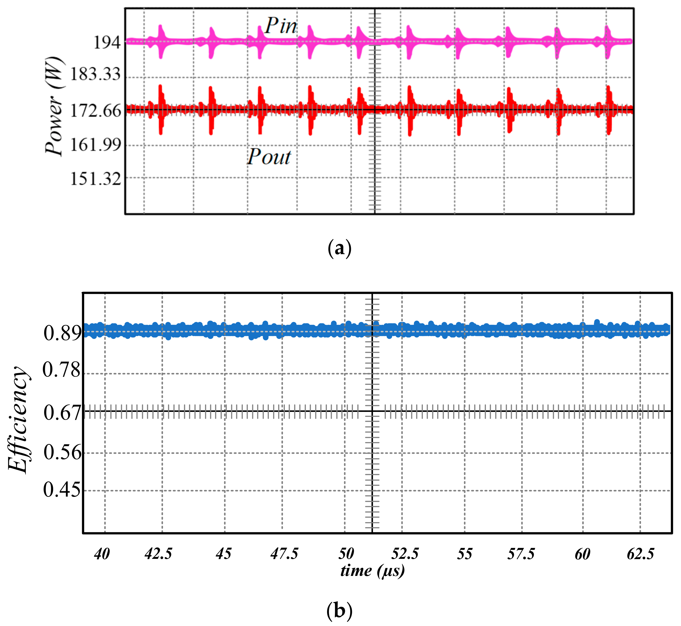
 Figure 7.
The key waveforms from the resonant tank in Figure 7 show the previously calculated overlap of M1 and M2. Alternatively, both the input current (iRe) and voltage (VRe) at the resonant tank show a condition close to resonance since both signals are in phase. Furthermore, the output voltage (Vr) is 207 V, which indicates that the parameters proposed in Table 2 have a relative error of 1.42% between them and the simulation results.
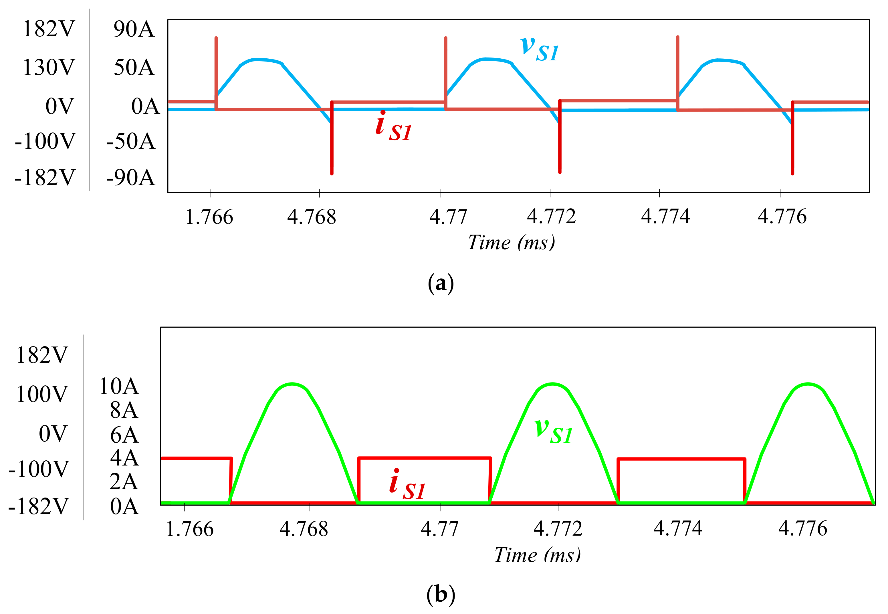
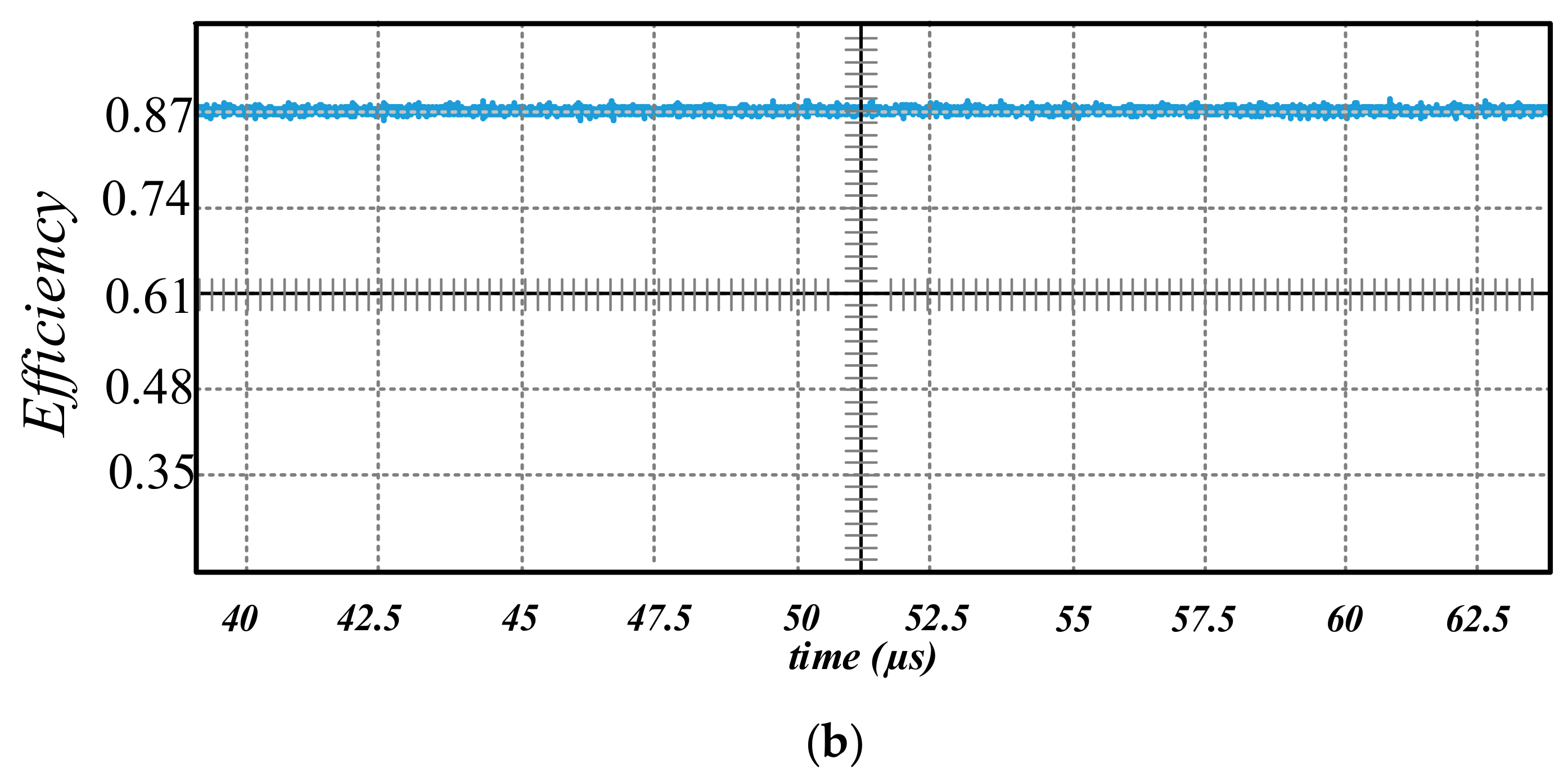
On the other hand, with the aim to compare the performance and conditions given for the topology, a comparison of a non-overlapped (Figure 8a) and overlapped control (Figure 8b) was made, focusing its attention on vS1 and iS1.
From Figure 8a, with a non-overlapped control, not only the voltage and current on S1, but also the resonance condition will be dramatically affected, causing negative voltages, as shown in Figure 8a. This issue would affect the entire efficiency because an overlap control provides a ramp shift signal to the ramp generator in response to a detection signal that indicates activity of the switches in the power stage. The ramp shift signal adjusts the first and second ramp signals relative to each other so as to minimize any gap and any overlap between the first and second ramp signals.
In this way, to have a good relation overlap-efficiency, an important point to consider is to work with an overlapped control to have optimal conditions, as shown in Figure 8b. Furthermore, Figure 8b shows less power losses as a result of the less current peaks obtained in comparison with the non-overlapped behavior presented in Figure 8a.

3. Experimental Results

Based on Table 2 and Table 3, the experimental prototype was elaborated. For experimental results, power devices used in the different combinations are shown in Table 4. Inductors were designed based on the Kg methodology [53], the PWM control optimized for high switching frequency, and the drivers used were UC3825 and MIC4452, respectively Furthermore, TD = 0.5 was considered. The elaborated prototype is shown in Figure 9.
Developing the experimental prototype at maximum power, the experimental results under different combinations of power devices are briefly described below by applying the OHMITE Rheostat RRS250E as a resistive load, which can be operated at a maximum ohmic and power value of 250 Ω and 500 W, respectively:

3.1. Overlap and Performed Efficiency by Si-Based Power Devices

For the first analysis, Figure 10 shows the overlapping signals (gate-source voltage) between M1 and M2.
From Figure 10, the performance given for silicon devices presents disturbances in the gate-signal modulation derived by the parasitic capacitance of each MOSFET. This noise will be reflected in the resonant tank. Moreover, S1 and S2 will be affected because of the reverse recovery current of D1 and D2, which will be reflected in the drain current of M1 and M2.
Additionally, it is well-known that Si power devices present a greater variation of non-linearity behavior of the output capacitance, whereas the low voltage part of the output capacitance increases due to higher area specific density. The high voltage part of the output capacitance decreases with the area shrink factor of the device, increasing the power losses and consequently affecting the overall performance of the converter. In this way, there is a need to study the performance given by new power devices technologies that permit a reduction of the high voltage part of the output capacitance leads to significant lower energy values being stored in it, because turning off Si devices with lossless would require to turn off the channel current before the voltage significantly rises across the device. The shape of the output capacitance, being charged by the full load current, will determine the voltage waveform. Conversely, the gain in the energy stored in the output capacitance, being dissipated as heat in hard switching applications during turn-on, is hence correlated to an increase of switching frequency. On the other hand, the overlapped signal in Figure 10 shows an operation frequency of ≈200 kHz, considering a duty cycle of 50%. In contrast, another important parameter is to determine the electrical efficiency; therefore, Figure 11a shows the input (Pin) and output power (Pout) as well as the efficiency (Figure 11b) obtained in the implemented topology.
According to the results, the converter efficiency is 83% and the loss is 32.8 W, which are significant. Additionally, as a result of the efficiency obtained with an optimized TD = 0.5, all losses were calculated to assess the electrical performance in all elements. To evaluate the passive elements, references [54] and [55] were used. In the case of capacitors, the loss is primarily from the equivalent series resistance (ESR), which is typically provided in the datasheet. Finally, the total power losses in MOSFETs are composed of switching and conduction losses; on the other hand, the total power losses in diodes are the sum of conduction, reverse, and switching losses. In this manner, Table 5 presents the total power losses on all elements of the experimental prototype, which parts of the estimated results were obtained from [34,36,55].
From Table 5, S1 and S2 present the higher total power losses, which indicates a similarity with the analysis presented in Section 2. Alternatively, in order to determine the distribution of power losses on the unidirectional switch, a study is presented in Section 4.

3.2. Overlap and Performed Efficiency by SiC-Based Power Devices

The second converter was developed by applying the second array of power devices. Figure 12 shows the gate-source voltage. Compared with Si devices, the overlap presented shows a reasonably better performance. The results show less disturbances in the gate-signal modulation derived by the parasitic capacitance of M1 and M2, since SiC devices present vertical current flow from the top surface to the bottom surface and have a blocking pn-junction with injection of bipolar carriers in reverse operation. In this sense, the reverse recovery charge is more than one magnitude lower than in corresponding silicon devices.
The results from Figure 12 make SiC components very suitable for applications with continuous hard commutation of the body diode as shown in the efficiency obtained (Figure 13b) according to the input and output power (Figure 13a). Furthermore, since the output capacitance is lower than in Si-based power devices, the stored energy in the output capacitance is comparable to GaN HEMTs semiconductors.
According to the results, the CFRC presents an incremented efficiency of 4% in comparison with Si devices. This results in 87% efficiency and losses of 26 W, which are quite significant. The distribution of these power losses is described in Table 6.
From Table 6, the performance given by SiC power devices presents a better performance in comparison with Si-based power technology. In fact, the percentage power reductions in comparison with the first array are shown in Table 7.
From Table 7, the components with the highest change are S1 and S2 with a considerable reduction of 27.84%, which results will be compared in Section 4.

3.3. Overlap and Performed Efficiency by GaN-Transistor and SiC-Diode

The third CFRC is designed considering the third array. Alternatively, since the topology under study is capable to works on a switching frequency of up to 200 kHz, a considerable reduction of the total power losses on the switch is not expected as a result of the reduction of the parasitic capacitance in the GaN-transistor. In this sense, the overlapping signals between M1 and M2 are shown in Figure 14.
Based on Figure 14, the overlap signals in M1 and M2 show a better performance by applying GaN-transistors because of the zero reverse recovery charge, which starts when the drain voltage falls below the sum of the gate potential and the threshold voltage, thus creating a reverse channel. This unique characteristic makes GaN-transistors the first choice for applications with continuous switching on a reverse biased device such as in half-bridge or full-bridge configurations. However, GaN power devices represent the best solution for high switching frequency applications. In this way, SiC power devices have similar efficiency and qualities by applying the same switching frequency in the CFRC presented in this work as shown in Figure 15.
According to Figure 15, the converter has an efficiency of 89% and losses of approximately 21.34 W.
The power losses distribution is presented in Table 8.
From Table 8, the performance given by the combination of GaN-transistor and SiC-diodes presents a better performance in comparison with Si and SiC-based power technologies.
In this way, the power reduction percentage in comparison with Si and SiC power devices are shown in Table 9 and Table 10, respectively.
From the comparison presented in Table 9, there is a considerable power reduction percentage as a result of the hybrid combination of GaN-transistor plus SiC-diode. Moreover, from the comparison in Table 10, the components with the highest change are S1 and S2 with a reduction of 21.43%. On the other hand, not only the losses in power devices are reduced but also in passive elements. The main reason is due to the input current ripple reduction, as shown in the input power ripple in Figure 11, Figure 13 and Figure 15, thus the conduction power losses are reduced. However, the converter electrical efficiency does not increase significantly and remains at approximately 89%. These results will be compared and analyzed in the following section.

4. Switching Loss Analysis

The switching losses of S1 and S2 for the different combinations of power devices consist of turn-on and turn-off loss, reverse recovery loss of the body diode, and output capacitance loss (Coss). The output capacitance loss effect is presented when S1 is in on-state because during both charging and discharging, the loss is generated. Therefore, the total additional loss caused by parasitic capacitances Coss from S1 and S2 estimated with the drain-source voltage charged is defined in (8).
E c a p = 1 2 C o s s S 1 V d c 2 + 1 2 C o s s S 2 V d c 2 = 1 2 C o s s t o t a l V d c 2
where Coss(total) = Coss(S1) + Coss(S2) is the total parasitic capacitance of the two switches. Therefore, regarding these issues and based on [56], Table 8 and Table 9 show the power loss distribution of S1 (MOSFET and diode) with TD = 0.5 by applying the different combinations of power devices. In this way, the results for S2 basically are the complementary losses of S1.
According to Table 11 and Table 12, the power losses in S1 and S2 considering TD = 0.5 show that 60% of the total power losses are caused by D1 and D2. This means that the primary problem caused by the use of unidirectional switches and overlap is related to the high voltages that will be absorbed by the parasitic capacitances of the power devices, increasing switching losses as a result of the diode in series with the MOSFET, preventing the MOSFET output capacitance from being discharged before the ZVS event.
Conversely, the percentage power reduction of GaN-transistor versus Si and SiC MOSFETs is approximately 66.49% and 53.57%, respectively. Additionally, the percentage power reduction of SiC-MOSFET, SiC-diode versus Si-MOSFET, Si-diode is around 27.84%.
As a result of the use of unidirectional switches in a CFRC, the switching stage will require power devices with low or zero reverse recovery charge, thus showing a clear value proposition for both GaN HEMTs and SiC devices, with both lower stored energies in the output capacitance, faster turn-off, and lower reverse recovery charge. On the other hand, GaN HEMTs power devices show better performance benefits as compared to their SiC counterparts by increasing the switching frequency. However, according to the topology under study, the use of both SiC and GaN power devices present a comprehensive similar performance.
As a result of the combination of Si, SiC, and GaN-based power devices in the CFRC applied to a PV-interconnected system in the DC-DC stage, at moderate switching frequencies, typically below 200 kHz, silicon carbide devices can compete. If switching frequencies move up to 400 kHz or above, the energy stored in the output capacitance will increases. In this case the value of GaN is significantly higher than its silicon counterparts. In fact, the benefits to the use of GaN power devices lies in its significantly lower charge stored in the output capacitance and its perfect linearity of the output capacitance. Additionally, the intrinsic capability to cope with hard commutation events in case of control errors is an additional benefit versus silicon and silicon carbide-based power devices.

5. Conclusions

This paper presents part of the key performance indicators for a CFRC combining Si, SiC, and GaN-based power devices. Regarding losses, one of the main problems associated with the low efficiency is related to the management that the overlap provides on the behavior of the unidirectional switch during the overlap the diode, preventing the MOSFET capacitance from being discharged.
The performance development by the unidirectional switches presents ZVS (Zero Voltage Switching) and ZCS (Zero Current Switching); however, hard switching appears when every device (MOSFET or diode) is analyzed independently. This issue is derived as a result of the energy losses in the parasitic capacitances of the MOSFET and diode. Furthermore, there is a recovery time on D1 and D2 in their shutdown states, generating that diodes are on-state even when the MOSFETs are off-state. Therefore, 60% of the total losses are generated by the diodes. Conversely, the percentage power reduction of GaN-transistor versus Si and SiC MOSFETs is approximately 66.49% and 53.57%, respectively. Additionally, the percentage power reduction of SiC-MOSFET plus SiC-diode versus Si-MOSFET plus Si-diode is around 27.84%.
The value proposition of SiC devices relies on the same arguments like for GaN devices with key performance indicators; however, not entirely reaching the level of corresponding GaN power devices for topologies that increase the switching frequency.
On the other hand, compared to conventional topologies, the proposed converter has continuous input current, and thus a capacitor in series with the photovoltaic panel is not necessary. Furthermore, the proposed converter does not present stability problems, and thanks to the arrangement of the parallel resonant tank, the topology provides galvanic isolation.

Author Contributions

Conceptualization, O.M.R.-B., M.P.-S. and J.A.A.-T.; data curation, O.M.R.-B., M.P.-S. and A.C.-S.; formal analysis, O.M.R.-B., M.P.-S., A.C.-S. and L.G.V.-V.; funding acquisition, M.P.-S., R.E.L.-P., and C.C.-G.; investigation, O.M.R.-B., M.P.-S. and J.A.A.-T.; methodology, M.P.-S., L.G.V.-V. and C.C.-G.; project administration, R.E.L.-P.; resources, O.M.R.-B., M.P.-S., A.C.-S. and L.G.V.-V.; software, O.M.R.-B., A.C.-S. and C.C.-G.; supervision, M.P.-S. and J.A.A.-T.; validation, O.M.R.-B., M.P.-S. and J.A.A.-T.; visualization, O.M.R.-B., M.P.-S., J.A.A.-T., A.C.-S. and L.G.V.-V.; writing—original draft, O.M.R.-B., M.P.-S. and J.A.A.-T.; writing—review & editing, R.E.L.-P., A.C.-S., L.G.V.-V. and C.C.-G. All authors have read and agreed to the published version of the manuscript.

Funding

This research was funded by Tecnologico Nacional de Mexico grant number (7746.20-P).

Conflicts of Interest

The authors declare no conflict of interest.

References

  1. Green, M.A.; Bremner, S.P. Energy conversion approaches and materials for high-efficiency photovoltaics. Nat. Mater. 2017, 16, 23–34. [Google Scholar] [CrossRef]
  2. Mahmud, M.; Pota, H.; Hossain, M. Nonlinear current control scheme for a single-phase grid-connected photovoltaic system. IEEE Trans. Sustain. Energy 2013, 5, 218–227. [Google Scholar] [CrossRef]
  3. Khan, R.; Khan, L.; Ullah, S.; Sami, I.; Ro, J.-S. Backstepping Based Super-Twisting Sliding Mode MPPT Control with Differential Flatness Oriented Observer Design for Photovoltaic System. Electronics 2020, 9, 1543. [Google Scholar] [CrossRef]
  4. Ko, J.-S.; Huh, J.-H.; Kim, J.-C. Overview of Maximum Power Point Tracking Methods for PV System in Micro Grid. Electronics 2020, 9, 816. [Google Scholar] [CrossRef]
  5. Mahdi, A.J.; Fahad, S.; Tang, W. An Adaptive Current Limiting Controller for a Wireless Power Transmission System Energized by a PV Generator. Electronics 2020, 9, 1648. [Google Scholar] [CrossRef]
  6. Selvaraj, J.; Rahim, N.A. Multilevel inverter for grid-connected PV system employing digital PI controller. Ieee Trans. Ind. Electron. 2008, 56, 149–158. [Google Scholar] [CrossRef]
  7. Padmanaban, S.; Blaabjerg, F.; Wheeler, P.; Ojo, J.O.; Ertas, A.H. High-voltage dc-dc converter topology for pv energy utilization—Investigation and implementation. Electr. Power Compon. Syst. 2017, 45, 221–232. [Google Scholar] [CrossRef]
  8. Fu, M.; Wang, Z.; Zhang, D.; Zhang, H. Isolated Boost Converter with High Efficiency and Wide Input/Output Voltage Range for Space Electric Propulsion System Applications. In Proceedings of the 2019 IEEE 2nd International Conference on Automation, Electronics and Electrical Engineering (AUTEEE), Shenyang, China, 22–24 November 2019; pp. 660–664. [Google Scholar]
  9. Wolski, K.; Zdanowski, M.; Rabkowski, J. High-frequency SiC-based inverters with input stages based on quasi-Z-source and boost topologies—Experimental comparison. IEEE Trans. Power Electron. 2019, 34, 9471–9478. [Google Scholar] [CrossRef]
  10. Jiang, S.; Cao, D.; Li, Y.; Peng, F.Z. Grid-connected boost-half-bridge photovoltaic microinverter system using repetitive current control and maximum power point tracking. IEEE Trans. Power Electron. 2012, 27, 4711–4722. [Google Scholar] [CrossRef]
  11. Chandwani, A.; Kothari, A. Design, simulation and implementation of Maximum Power Point Tracking (MPPT) for solar based renewable systems. In Proceedings of the 2016 International Conference on Electrical Power and Energy Systems (ICEPES), Bhopal, India, 14–16 December 2016; pp. 539–544. [Google Scholar]
  12. Arunkumari, T.; Indragandhi, V. A review on single switch Dc-Dc converter for renewable energy based applications. In Proceedings of the 2017 Innovations in Power and Advanced Computing Technologies (i-PACT), Vellore, India, 21–22 April 2017; pp. 1–5. [Google Scholar]
  13. Reshma, R.; Selvakumar, S.V. A soft switching dual flyback DC-DC converter for renewable energy applications. Int. J. Adv. Res. Ideas Innov. Technol. 2018, 4, 1050–1053. [Google Scholar]
  14. Bhosale, H.C.; Kale, R.; Harchandani, R. Significant Role, Design and Stability Analysis of Flyback Converter for Renewable Energy Source. In Proceedings of the 2019 International Conference on Advances in Computing, Communication and Control (ICAC3), Mumbai, India, 20–21 December 2019; pp. 1–5. [Google Scholar]
  15. Jiménez-Martínez, J.M.; Bonilla, E.D.J.; Aroca, A.M.; Mañas, J.A.V. Improving passive current sharing in multiphase active-clamp flyback converter with high step-up ratio. In Proceedings of the 2017 19th European Conference on Power Electronics and Applications (EPE’17 ECCE Europe), Warsaw, Poland, 11–14 September 2017; pp. P.1–P.7. [Google Scholar]
  16. Alghaythi, M.L.; O’Connell, R.M.; Islam, N.E. Design of a High Step-up DC-DC Power Converter with Voltage Multiplier Cells and Reduced Losses on Semiconductors for Photovoltaic Systems. In Proceedings of the 2019 IEEE Electric Ship Technologies Symposium (ESTS), Arlington, VA, USA, 14–16 August 2019; pp. 214–218. [Google Scholar]
  17. Gu, Y.; Lu, Z.; Hang, L.; Qian, Z.; Huang, G. Three-level LLC series resonant DC/DC converter. IEEE Trans. Power Electron. 2005, 20, 781–789. [Google Scholar] [CrossRef]
  18. Yi, K.-H.; Moon, G.-W. Novel two-phase interleaved LLC series-resonant converter using a phase of the resonant capacitor. IEEE Trans. Ind. Electron. 2009, 56, 1815–1819. [Google Scholar]
  19. Liang, Z.; Guo, R.; Wang, G.; Huang, A. A new wide input range high efficiency photovoltaic inverter. In Proceedings of the 2010 IEEE Energy Conversion Congress and Exposition, Atlanta, GA, USA, 12–16 September 2010; pp. 2937–2943. [Google Scholar]
  20. Beiranvand, R.; Zolghadri, M.R.; Rashidian, B.; Alavi, S.M.H. Optimizing the LLC–LC resonant converter topology for wide-output-voltage and wide-output-load applications. IEEE Trans. Power Electron. 2011, 26, 3192–3204. [Google Scholar] [CrossRef]
  21. Fang, X.; Hu, H.; Chen, F.; Somani, U.; Auadisian, E.; Shen, J.; Batarseh, I. Efficiency-oriented optimal design of the LLC resonant converter based on peak gain placement. IEEE Trans. Power Electron. 2012, 28, 2285–2296. [Google Scholar] [CrossRef]
  22. Feng, W.; Lee, F.C.; Mattavelli, P. Simplified optimal trajectory control (SOTC) for LLC resonant converters. IEEE Trans. Power Electron. 2012, 28, 2415–2426. [Google Scholar] [CrossRef]
  23. Hu, H.; Fang, X.; Chen, F.; Shen, Z.J.; Batarseh, I. A modified high-efficiency LLC converter with two transformers for wide input-voltage range applications. IEEE Trans. Power Electron. 2012, 28, 1946–1960. [Google Scholar] [CrossRef]
  24. Musavi, F.; Craciun, M.; Gautam, D.S.; Eberle, W.; Dunford, W.G. An LLC resonant DC–DC converter for wide output voltage range battery charging applications. IEEE Trans. Power Electron. 2013, 28, 5437–5445. [Google Scholar] [CrossRef]
  25. Wang, D.; Liu, Y.-F. A zero-crossing noise filter for driving synchronous rectifiers of LLC resonant converter. IEEE Trans. Power Electron. 2013, 29, 1953–1965. [Google Scholar] [CrossRef]
  26. Lin, B.-R.; Wang, K.-W. Interleaved soft switching resonant converter with a small input ripple current. Int. J. Electron. 2020, 107, 644–658. [Google Scholar] [CrossRef]
  27. Chu, C.-L.; Li, C.-H. Analysis and design of a current-fed zero-voltage-switching and zero-current-switching CL-resonant push–pull dc–dc converter. IET Power Electron. 2009, 2, 456–465. [Google Scholar] [CrossRef]
  28. Sun, X.; Shen, Y.; Zhu, Y.; Guo, X. Interleaved boost-integrated LLC resonant converter with fixed-frequency PWM control for renewable energy generation applications. IEEE Trans. Power Electron. 2014, 30, 4312–4326. [Google Scholar] [CrossRef]
  29. Kumar, M.S.R.; Amudha, A.; Rajeev, R. Optimization for A Novel Single Switch Resonant Power Converter Using Ga To Improve MPPT Efficiency of PV Applications. Int. J. Appl. Eng. Res. 2016, 11, 6485–6488. [Google Scholar]
  30. Lin, B.-R.; Lin, Y. Parallel current-fed resonant converter with balance current sharing and no input ripple current. IET Power Electron. 2018, 12, 212–219. [Google Scholar] [CrossRef]
  31. Flourentzou, N.; Agelidis, V.G.; Demetriades, G.D. VSC-based HVDC power transmission systems: An overview. IEEE Trans. Power Electron. 2009, 24, 592–602. [Google Scholar] [CrossRef]
  32. Ponce-Silva, M.; Bautista, J.L.; Tapia, A.; Nicolas, C.I.; Granados, T.R.; Araujo, I. Parallel-resonant inverter with two current sources: Analysis and design methodology. In Proceedings of the Power Electronics Congress (CIEP), 2010 12th International, San Luis Potosí, México, 22–25 August 2010; pp. 156–160. [Google Scholar]
  33. Wang, C.-L.; Yu, C.-S.; Wong, P.-T. Unidirectional MOSFET and Applications Thereof. Google Patents US8363437B2, 2013. [Google Scholar]
  34. Kazimierczuk, M.K.; Cravens, R. Current-source parallel-resonant DC/AC inverter with transformer. IEEE Trans. Power Electron. 1996, 11, 275–284. [Google Scholar] [CrossRef]
  35. Yunus, H.I.; Bass, R.M. Comparison of VSI and CSI topologies for single-phase active power filters. In Proceedings of the PESC Record. 27th Annual IEEE Power Electronics Specialists Conference, Baveno, Italy, 23–27 June 1996; pp. 1892–1898. [Google Scholar]
  36. Kazimierczuk, M.K. High-Frequency Magnetic Components; John Wiley & Sons: Hoboken, NJ, USA, 2009. [Google Scholar]
  37. Dimitrijev, S.; Jamet, P. Advances in SiC power MOSFET technology. Microelectron. Reliab. 2003, 43, 225–233. [Google Scholar] [CrossRef]
  38. Tsuchida, H.; Kamata, I.; Miyazawa, T.; Ito, M.; Zhang, X.; Nagano, M. Recent advances in 4H-SiC epitaxy for high-voltage power devices. Mater. Sci. Semicond. Process. 2018, 78, 2–12. [Google Scholar] [CrossRef]
  39. Umezawa, H. Recent advances in diamond power semiconductor devices. Mater. Sci. Semicond. Process. 2018, 78, 147–156. [Google Scholar] [CrossRef]
  40. Fardi, H.Z.; Alaghband, G.; Pankove, J.I. Numerical modelling and characterization of high-frequency high-power high-temperature GaN/SiC heterostructure bipolar transistors. Int. J. Electron. 1997, 82, 567–574. [Google Scholar] [CrossRef]
  41. Zhang, A.; Ren, F.; Anderson, T.; Abernathy, C.; Singh, R.; Holloway, P.; Pearton, S.; Palmer, D.; McGuire, G. High-power GaN electronic devices. Crit. Rev. Solid State Mater. Sci. 2002, 27, 1–71. [Google Scholar] [CrossRef]
  42. Duan, B.; Yang, Y. A development summarization of the power semiconductor devices II. IETE Tech. Rev. 2012, 29, 36–43. [Google Scholar] [CrossRef]
  43. Guo, H.; Duan, B.; Wu, H.; Yang, Y. Breakdown mechanisms of power semiconductor devices. IETE Tech. Rev. 2018, 36, 243–252. [Google Scholar] [CrossRef]
  44. Shenai, K.; Scott, R.S.; Baliga, B.J. Optimum semiconductors for high-power electronics. IEEE Trans. Electron Devices 1989, 36, 1811–1823. [Google Scholar] [CrossRef]
  45. Roccaforte, F.; Fiorenza, P.; Greco, G.; Vivona, M.; Nigro, R.L.; Giannazzo, F.; Patti, A.; Saggio, M. Recent advances on dielectrics technology for SiC and GaN power devices. Appl. Surf. Sci. 2014, 301, 9–18. [Google Scholar] [CrossRef]
  46. Dimitrijev, S.; Han, J.; Moghadam, H.A.; Aminbeidokhti, A. Power-switching applications beyond silicon: Status and future prospects of SiC and GaN devices. Mrs Bull. 2015, 40, 399–405. [Google Scholar] [CrossRef]
  47. Deboy, G.; Treu, M.; Häberlen, O.; Neumayr, D. Si, SiC and GaN power devices: An unbiased view on key performance indicators. In Proceedings of the 2016 IEEE International Electron Devices Meeting (IEDM), San Francisco, CA, USA, 3–7 December 2017. [Google Scholar]
  48. Flack, T.J.; Pushpakaran, B.N.; Bayne, S.B. GaN technology for power electronic applications: A review. J. Electron. Mater. 2016, 45, 2673–2682. [Google Scholar] [CrossRef]
  49. Shah, F.M.; Xiao, H.M.; Li, R.; Awais, M.; Zhou, G.; Bitew, G.T. Comparative performance evaluation of temperature dependent characteristics and power converter using GaN, SiC and Si power devices. In Proceedings of the 2018 IEEE 12th International Conference on Compatibility, Power Electronics and Power Engineering (CPE-POWERENG 2018), Doha, Qatar, 10–12 April 2018; pp. 1–7. [Google Scholar]
  50. Georgiev, A.; Papanchev, T.; Nikolov, N. Reliability assessment of power semiconductor devices. In Proceedings of the 2016 19th International Symposium on Electrical Apparatus and Technologies (SIELA), Bourgas, Bulgaria, 29 May–1 June; pp. 1–4.
  51. Ji, S.; Zhang, Z.; Wang, F. Overview of high voltage SiC power semiconductor devices: Development and application. CES Trans. Electr. Mach. Syst. 2017, 1, 254–264. [Google Scholar] [CrossRef]
  52. Huang, A.Q. Power semiconductor devices for smart grid and renewable energy systems. Power Electron. Renew. Energy Syst. Smart Grid Technol. Appl. 2019, 85–152. [Google Scholar] [CrossRef]
  53. Erickson, R.W.; Maksimovic, D. Fundamentals of Power Electronics; Springer Science & Business Media: New York, NY, USA, 2007. [Google Scholar]
  54. Li, J.; Abdallah, T.; Sullivan, C.R. Improved calculation of core loss with nonsinusoidal waveforms. In Proceedings of the Conference Record of the 2001 IEEE Industry Applications Conference: 36th IAS Annual Meeting (Cat. No. 01CH37248), Chicago, IL, USA, 30 September–4 October 2001; pp. 2203–2210. [Google Scholar]
  55. Kazimierczuk, M. Winding resistance at high frequencies. High.-Freq. Magn. Compon. 2014, 265–325. [Google Scholar]
  56. Maniktala, S. Switching Power Supplies A-Z; Elsevier: Oxford, UK, 2012. [Google Scholar]
Figure 1. Current-fed DC-DC resonant converters (CFRC) performing unidirectional switches using a metal–oxide–semiconductor field-effect transistor (MOSFET) in series with a diode.
Electronics 09 01982 g001
Figure 2. Simulation key waveforms: (a) voltage and current in switch S1 (vS1 and iS1), (b) voltage and current in switch S2 (vS2 and iS2), (c) voltage and current at the diode D1 (VD1 and iD1), (d) gate-signal in M1 (VGSM1) and gate-signal in M2 (VGSM2), (e) drain-source voltage and current at the MOSFET M1 (vM1 and iM1).
Electronics 09 01982 g002
Figure 3. Key waveforms: voltage and current in S1 and S2.
Electronics 09 01982 g003
Figure 4. Equivalent circuits; (a) from t0t1, (b) from t1t2, (c) from t2t3, (d) from t3t4.
Electronics 09 01982 g004aElectronics 09 01982 g004b
Figure 5. Overlapped signals in M1 and M2.
Electronics 09 01982 g005
Figure 6. Efficiency versus time delay (TD) with different power devices.
Electronics 09 01982 g006
Figure 7. Waveforms of the DC-DC resonant converter: gate-signals (VGSM1 and VGSM2), input voltage, and current at the resonant tank (iRe and VRe) and output voltage (Vr).
Electronics 09 01982 g007
Figure 8. Signals: (a) current and voltage on S1 with a non-overlapped control, (b) current and voltage on S1 with an overlapped control.
Electronics 09 01982 g008
Figure 9. Current fed DC-DC resonant converter implemented.
Electronics 09 01982 g009
Figure 10. Overlapping signals performed for the first array.
Electronics 09 01982 g010
Figure 11. Electrical signals implemented by the first array: (a) input and output power, and (b) efficiency.
Electronics 09 01982 g011
Figure 12. Overlapping signals performed for the second array.
Electronics 09 01982 g012
Figure 13. Electrical signals of the second array (a) input and output power, (b) efficiency implemented.
Electronics 09 01982 g013aElectronics 09 01982 g013b
Figure 14. Overlapping signals performed for the third array.
Electronics 09 01982 g014
Figure 15. Electrical signals of the third array (a) input and output power, (b) efficiency implemented.
Electronics 09 01982 g015
Table 1. Physical properties of silicon (Si), silicon carbide (SiC), and gallium nitride (GaN).
Electrical PropertyUnitsSiSiCGaN
Band gap energy eV 1.13.263.4
Thermal conduction W / cm · K 1.53.71.3
Electron mobility cm 2 /   V ·s1300900900–2000
Saturation drift velocity cm / s 1 × 10 7 2 × 10 7 2.5 × 10 7
Table 2. Design parameters.
ParameterSymbolValue
Output power P W 200
Input voltage V D C ( V ) 30.3
Switching frequency F s w kHz 200
Quality factor Q 5
Output voltage V r V 210
Rectifier voltage V A B V 267.38
Angular frequency ω r Hz 1,257,000
Table 3. Design methodology.
ParameterSymbolEquationValue
Load R l o a d V r 2 P l o a d 213.8 Ω
Current sources L 1 , L 2 v c c 2 0.2 P g r i d F s w 114.8 μH
Resonant capacitor C R Q 2 π 60 R e q u 186.7 nF
Number of turns n n = 1 V D C π 2 P l o a d R e q u η r e s 3.588
Secondary winding L Sec o n d a r y 1 ω r 2 C r 3.392 µH
Primary winding L Pr i m a r y n 2 L s 43.66 µH
Decoupling inductance L c V A B 4 F s w 0.199 3 mH
Decoupling capacitor C c 1 D V r 8 L b F s w 2 Δ v o 5 µF
Table 4. Characteristics of the power semiconductor devices.
ModelDeviceCharacteristicsMaterial
EPC2007CTransistorVDS (V)100GaN
ID (A)6
RDS(on) (Ω)0.03
C2M0160120DMOSFETVDS (V)1200SiC
ID (A)19
RDS(on) (Ω)0.160
C4D08120DiodeVRRM (V)1200SiC
IF (A)6.4
TJ (°C)175
STF12N120K5MOSFETVDS (V)1200Si
ID (A)12
RDS(on) (Ω)0.69
STTH812DiodeVRRM (V)1200Si
IF (A)8
TJ (°C)175
Table 5. Total power losses distribution by applying Si power devices.
ComponentPower Losses (W)
Current source L1 and L21.2
Inductor LC1.33
Rectifier4
Transformer4.2
S1 and S219.4
Stage control and wiring2.7
Table 6. Total power losses distribution by applying SiC power devices.
ComponentPower Losses (W)
Current source L1 and L21.1
Inductor LC1.31
Rectifier3
Transformer4
S1 and S214
Stage control and wiring2.56
Table 7. Power reduction percentage; first vs. second array.
SiC Vs. SiL1 and L2LC InductorRectifierTransformerS1 and S2Stage Control
8.33%1.50%25.00%4.76%27.84%5.19%
Table 8. Total power losses by applying GaN and SiC power devices.
ComponentPower Losses (W)
Current source L1 and L21
Inductor LC1.265
Rectifier3
Transformer3
S1 and S211
Stage control and wiring2.12
Table 9. Power reduction percentage; first vs. third array.
GaN Vs. SiL1 and L2LCInductorRectifierTransformerS1 and S2Stage Control
16.674.8925.0028.5743.3021.48
Table 10. Power reduction percentage; second vs. third array.
GaN Vs. SiCL1 and L2LC InductorRectifierTransformerS1 and S2Stage Control
9.093.440.0025.0021.4317.19
Table 11. Power losses distribution in MOSFET M1.
ComponentPSwitching (W)PConduction (W)Total (W)Material
STB57N65M50.7763.1043.88Si
C2M0160120D0.562.242.8SiC
EPC2007C0.261.041.3GaN
Table 12. Power losses distribution in diode D1.
ComponentPSwitching (W)PConduction (W)PReverse (W)Total (W)Material
DSS17-06CR0.5822.912.3285.82Si
C4D081200.422.11.684.2SiC
Publisher’s Note: MDPI stays neutral with regard to jurisdictional claims in published maps and institutional affiliations.

